 | –≠–ª–µ–∫—Ç—Ä–æ–Ω–Ω—ã–π –∫–æ–º–ø–æ–Ω–µ–Ω—Ç: EL2082C | –°–∫–∞—á–∞—Ç—å:  PDF PDF  ZIP ZIP |
EL2082C
January
1996
Rev
D
EL2082C
Current-Mode Multiplier
Note All information contained in this data sheet has been carefully checked and is believed to be accurate as of the date of publication however this data sheet cannot be a ``controlled document'' Current revisions if any to these
specifications are maintained at the factory and are available upon your request We recommend checking the revision level before finalization of your design documentation
1992 Elantec Inc
Features
Flexible inputs and outputs all
ground referred
150 MHz large and small-signal
bandwidth
46 dB of calibrated gain control
range
70 dB isolation in disable mode
10 MHz
0 15% diff gain and 0 05 diff
phase performance at NTSC
using application circuit
Operates on
g
5V to
g
15V power
supplies
Outputs may be paralleled to
function as a multiplexer
Applications
Level adjust for video signals
Video faders and mixers
Signal routing multiplexers
Variable active filters
Video monitor contrast control
AGC
Receiver IF gain control
Modulation demodulation
General ``cold'' front-panel
control of AC signals
Ordering Information
Part No
Temp Range
Package
Outline
EL2082CN
0 C to
a
75 C
8-Pin P-DIP
MDP0031
EL2082CS
0 C to
a
75 C
8-Pin SO
MDP0027
General Description
The EL2082 is a general purpose variable gain control building
block built using an advanced proprietary complementary bi-
polar process It is a two-quandrant multiplier so that zero or
negative control voltages do not allow signal feedthrough and
very high attenuation is possible The EL2082 works in current
mode rather than voltage mode so that the input impedance is
low and the output impedance is high This allows very wide
bandwidth for both large and small signals
The I
IN
pin replicates the voltage present on the V
IN
pin there-
fore the V
IN
pin can be used to reject common-mode noise and
establish an input ground reference The gain control input is
calibrated to 1 mA mA signal gain for 1V of control voltage
The disable pin (E) is TTL-compatible and the output current
can comply with a wide range of output voltages
Because current signals rather than voltages are employed mul-
tiple inputs can be summed and many outputs wire-or'ed or
mixed
The EL2082 operates from a wide range of supplies and is avail-
able in standard 8-pin plastic DIP or 8-lead SO
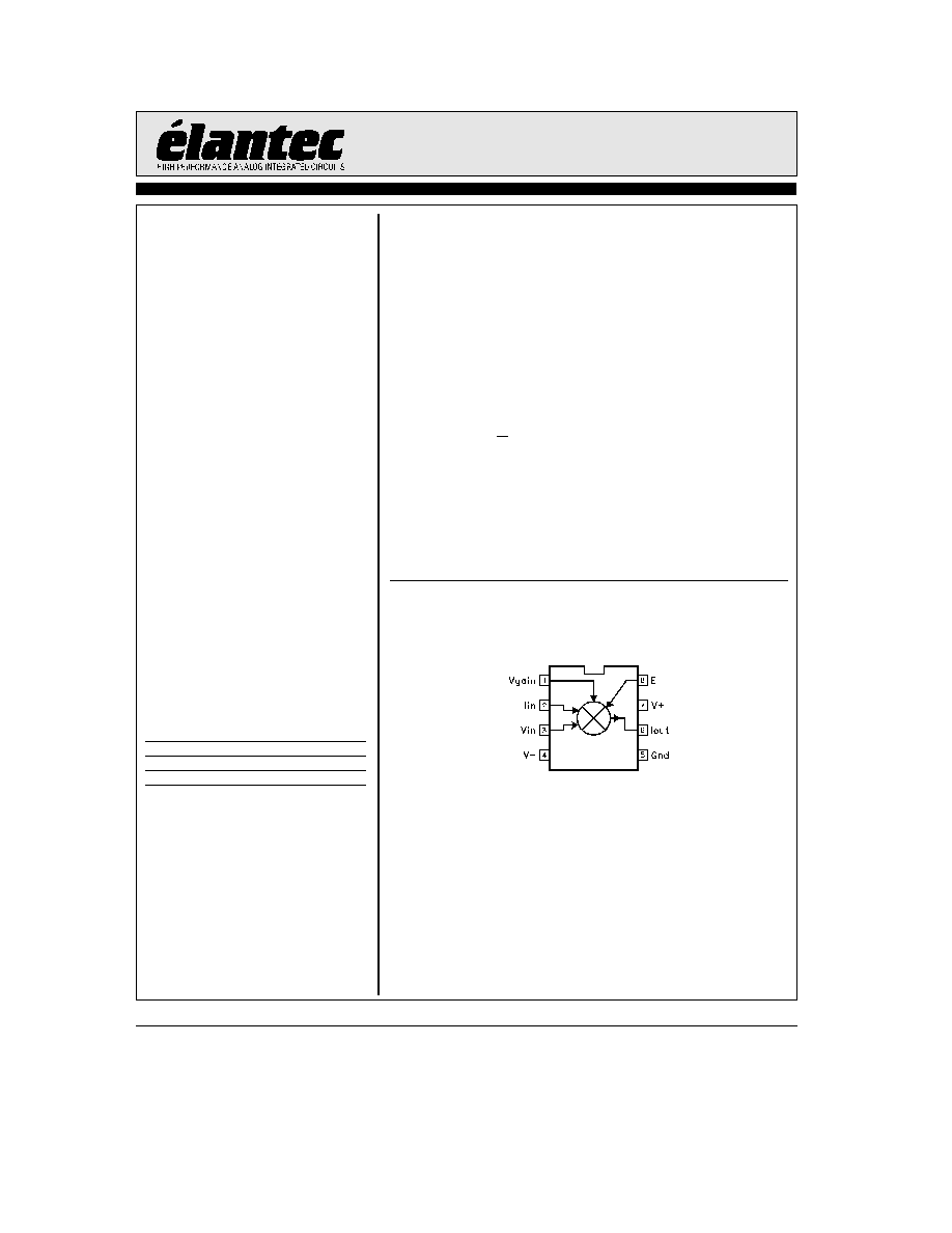
Connection Diagram
8-Pin DIP SO
2082 ≠ 1
Top View

EL2082C
Current-Mode Multiplier
Absolute Maximum Ratings
(T
A
e
25 C)
V
S
Voltage between V
S
a
and V
S
b
a
33V
V
IN
I
OUT
Voltage
g
V
S
V
E
V
GAIN
Input Voltage
b
1 to
a
7V
I
IN
Input Current
g
5 mA
P
D
Maximum Power Dissipation
See Curves
T
A
Operating Temperature Range
0 C to
a
75 C
T
J
Operating Junction Temperature
150 C
T
ST
Storage Temperature
b
65 C to
a
150 C
Important Note
All parameters having Min Max specifications are guaranteed The Test Level column indicates the specific device testing actually
performed during production and Quality inspection Elantec performs most electrical tests using modern high-speed automatic test
equipment specifically the LTX77 Series system Unless otherwise noted all tests are pulsed tests therefore T
J
e
T
C
e
T
A
Test Level
Test Procedure
I
100% production tested and QA sample tested per QA test plan QCX0002
II
100% production tested at T
A
e
25 C and QA sample tested at T
A
e
25 C
T
MAX
and T
MIN
per QA test plan QCX0002
III
QA sample tested per QA test plan QCX0002
IV
Parameter is guaranteed (but not tested) by Design and Characterization Data
V
Parameter is typical value at T
A
e
25 C for information purposes only
DC Electrical Characteristics
(V
S
e
g
15V V
G
e
1V V
E
e
0 8V V
OUT
e
0 V
IN
e
0 I
IN
e
0)
Parameter
Description
Temp
Min
Typ
Max
Test
Units
Level
V
IO
Input Offset Voltage
Full
b
20
20
II
mV
I
OO
Output Offset Current
Full
b
100
100
II
mA
R
INI
I
IN
Input Impedance I
IN
e
0 0 35 mA
Full
75
95
115
II
X
V
CMRR
Voltage Common-Mode Rejection Ratio
Full
45
55
II
dB
V
IN
e b
10V
a
10V
I
CMRR
Offset Current Common-Mode Rejection
Full
0 5
5
II
mA V
Ratio V
IN
e b
10V
a
10V
V
PSRR
Offset Voltage Power Supply Rejection
Full
60
80
II
dB
Ratio V
S
e
g
5V to
g
15V
I
PSRR
Offset Current Power Supply Rejection
Full
1
10
II
mA V
Ratio V
S
e
g
5V to
g
15V
I
BVIN
V
IN
Bias Current
Full
b
10
10
II
mA
R
INV
V
IN
Input Impedance V
IN
e b
10V
a
10V
Full
0 5
1 0
II
M
X
Nlini
Signal Nonlinearity I
IN
e b
0 7 mA
Full
0 10
0 4
II
%
b
0 35 mA 0 mA
a
0 35 mA
a
0 7 mA
R
OUT
Output Impedance V
OUT
e b
10V
a
10V
Full
0 25
0 5
II
M
X
2
TD
is
30in

EL2082C
Current-Mode Multiplier
DC Electrical Characteristics
Contd
(V
S
e
g
15V V
G
e
1V V
E
e
0 8V V
OUT
e
0 V
IN
e
0 I
IN
e
0)
Parameter
Description
Temp
Min
Typ
Max
Test
Units
Level
V
OUT
Output Swing V
GAIN
e
2V I
IN
g
2 mA
Full
b
11
a
11
II
V
R
L
e
4 0K
V
IOG
V
OS
Gain Control Extrapolated
Full
b
15
15
II
mV
from V
GAIN
e
0 1V 1V
A
I
Current Gain I
IN
g
350
mA
Full
0 9
1 0
1 1
II
mA mA
Nling
Nonlinearity of Gain Control
Full
2
5
II
%
V
GAIN
e
0 1V 0 5V 1V
I
SO
Input Isolation with V
GAIN
e b
0 1V
Full
b
80
b
96
II
dB
V
INH
E Logic High Level
Full
2 0
II
V
V
INL
E Logic Low Level
Full
0 8
II
V
I
LH
Input Current of E V
E
e
5V
Full
b
50
50
II
mA
I
LL
Input Current of E V
E
e
0
Full
b
50
50
II
mA
I
ODIS
I
OUT
Disabled E
e
2 0V
Full
g
10
II
mA
I
S
Supply Current
Full
13
16
II
mA
AC Electrical Characteristics
(R
L
e
25
X C
L
e
4 pF C
IIN
e
2 pF T
A
e
25 C V
G
e
1V V
S
e
g
15V)
Parameter
Description
Min
Typ
Max
Test
Units
Level
BW1
Current Mode Bandwidth
b
3 dB
150
V
MHz
BW2
g
0 1 dB
30
V
MHz
BWp
Power I
IN
e
1 mA p-p
150
V
MHz
BWg
Gain Control Bandwidth
20
V
MHz
SRG
Gain Control Slew Rate
V
G
from 0 2V to 2V
12
V
(mA mA)
ms
T
REC
Recovery Time from V
G
k
0
250
V
ns
T
EN
Enable Time from E Pin
200
V
ns
T
DIS
Disable Time from E Pin
30
V
ns
D
G
Differential Gain
0 25
V
%
NTSC with I
IN
e b
0 35 mA to
a
0 35 mA
D
P
Differential Phase
0 05
V
Degree
NTSC with I
IN
e b
0 35 mA to
a
0 35 mA
3
TD
is
28in
TD
is
24in

EL2082C
Current-Mode Multiplier
Typical Performance Curves
Frequency for Different Gains
Current Gain vs
vs Frequency
Current Gain
Current Gain Flatness
Voltage Input Mode
Frequency Response in
Input Amplitude
Harmonic Distortion vs
vs Frequency
Output Current Noise
2082 ≠ 2
4

EL2082C
Current-Mode Multiplier
Typical Performance Curves
Contd
vs DC Offset Current
Differential Gain Error
DC Offset Current
Differential Phase Error vs
2082 ≠ 3
Gain Pin Transient Response
2082 ≠ 4
Gain Control Recovery From
Vg e b0 1V
2082 ≠ 5
Frequency Response
Gain Control Pin
I
OUT
vs I
IN
vs V
GAIN
Voltage
Normalized Gain Error
2082 ≠ 6
5