 | –≠–ª–µ–∫—Ç—Ä–æ–Ω–Ω—ã–π –∫–æ–º–ø–æ–Ω–µ–Ω—Ç: EL2130CN | –°–∫–∞—á–∞—Ç—å:  PDF PDF  ZIP ZIP |
EL2130C
December
1995
Rev
C
EL2130C
85 MHz Current Feedback Amplifier
Note All information contained in this data sheet has been carefully checked and is believed to be accurate as of the date of publication however this data sheet cannot be a ``controlled document'' Current revisions if any to these
specifications are maintained at the factory and are available upon your request We recommend checking the revision level before finalization of your design documentation
1990 Elantec Inc
Features
b
3 dB bandwidth
e
85 MHz
A
V
e
1
b
3 dB bandwidth
e
75 MHz
A
V
e
2
NTSC PAL dG
s
0 03% dP
s
0 1
50 mA output current
Drives
g
2 5V into 100
X load
Low voltage noise
e
4 nV
0
Hz
Current mode feedback
Low cost
Applications
Video amplifier
Video distribution amplifier
Residue amplifiers in ADC
Current to voltage converter
Coaxial cable driver
Ordering Information
Part No
Temp Range
Pkg
Outline
EL2130CN 0 C to a75 C
8-Pin P-DIP MDP0031
EL2130CS 0 C to a75 C
8-Lead SO
MDP0027
General Description
The EL2130 is a wideband current mode feedback amplifier op-
timized for gains between
b
10 and
a
10 while operating on
g
5V power supplies Built using Elantec's Complementary Bi-
polar process this device exhibits
b
3 dB bandwidths in excess
of 85 MHz at unity gain and 75 MHz at a gain of two The
EL2130 is capable of output currents in excess of 50 mA giving
it the ability to drive either double or single terminated 50
X
coaxial cables
Exhibiting a Differential Gain of 0 03% and a Differential
Phase of 0 1 at NTSC and PAL frequencies The EL2130 is an
excellent low cost solution to most video applications
In addition the EL2130 exhibits very low gain peaking typical-
ly below 0 1 dB to frequencies in excess of 40 MHz as well as 50
ns settling time to 0 2% making it an excellent choice for driv-
ing flash A D converters
The device is available in the plastic 8-lead narrow-body small
outline (SO) and the 8-pin mini DIP packages and operates
over the temperature range of 0 C to
a
75 C
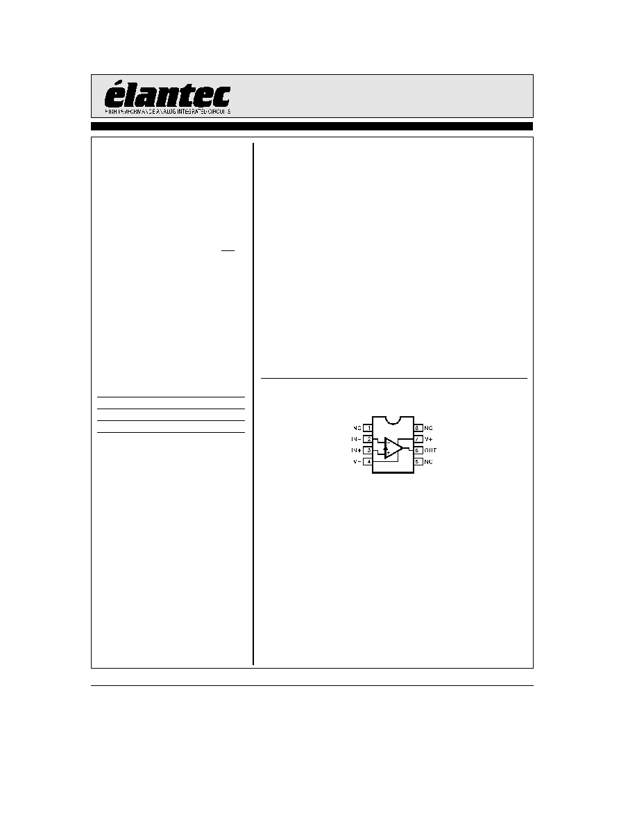
Connection Diagram
Mini DIP and SO
2130 ≠ 1
Manufactured under U S Patent No 4 893 091

EL2130C
85 MHz Current Feedback Amplifier
Absolute Maximum Ratings
(T
A
e
25 C)
V
S
Supply Voltage
g
6V
V
IN
Input Voltage
g
V
S
DV
IN
Differential Input Voltage
g
6V
P
D
Maximum Power Dissipation
See Curves
I
IN
Input Current
g
10 mA
I
OP
Output Short Circuit Duration
s
5 sec
T
A
Operating Temperature Range
0 C to
a
75 C
T
J
Operating Junction Temperature
150 C
T
ST
Storage Temperature
b
65 C to
a
150 C
Important Note
All parameters having Min Max specifications are guaranteed The Test Level column indicates the specific device testing actually
performed during production and Quality inspection Elantec performs most electrical tests using modern high-speed automatic test
equipment specifically the LTX77 Series system Unless otherwise noted all tests are pulsed tests therefore T
J
e
T
C
e
T
A
Test Level
Test Procedure
I
100% production tested and QA sample tested per QA test plan QCX0002
II
100% production tested at T
A
e
25 C and QA sample tested at T
A
e
25 C
T
MAX
and T
MIN
per QA test plan QCX0002
III
QA sample tested per QA test plan QCX0002
IV
Parameter is guaranteed (but not tested) by Design and Characterization Data
V
Parameter is typical value at T
A
e
25 C for information purposes only
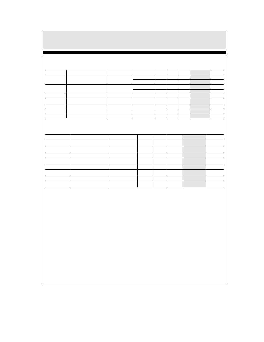
Open Loop DC Electrical Characteristics
V
S
e
g
5V R
L
e
%
unless otherwise specified
Parameter
Description
Condition
Temp
Min
Typ
Max
Test Level
Units
V
OS
Input Offset Voltage
25 C
2 0
10
I
mV
T
MIN
T
MAX
15
III
mV
DV
OS
DT
Offset Voltage Drift
7
V
mV C
a
I
IN
a
Input Current
25 C
5 5
15
I
mA
T
MIN
T
MAX
25
III
mA
b
I
IN
a
Input Current
25 C
10
40
I
mA
T
MIN
T
MAX
50
III
mA
a
R
IN
a
Input Resistance
25 C
1 0
2 0
I
M
X
C
IN
a
Input Capacitance
25 C
1 0
V
pF
CMRR
Common Mode
V
CM
e
g
2 5V
25 C
50
60
I
dB
Rejection Ratio
b
ICMR
Input Current Common
V
CM
e
g
2 5V
25 C
5
10
I
mA V
Mode Rejection
T
MIN
T
MIN
20
III
mA V
PSRR
Power Supply Rejection
g
4 5V
s
V
S
s g
6V
25 C
60
70
I
dB
Ratio
a
IPSR
a
Input Current Power
g
4 5V
s
V
S
s g
6V
25 C
0 1
0 5
I
mA V
Supply Rejection
T
MIN
T
MIN
1 0
III
mA V
b
IPSR
b
Input Current Power
g
4 5V
s
V
S
s g
6V
25 C
0 5
5 0
I
mA V
Supply Rejection
T
MIN
T
MIN
8 0
III
mA V
2
TD
is
30in
EL2130C
85 MHz Current Feedback Amplifier
Open Loop DC Electrical Characteristics
V
S
e
g
5V R
L
e
%
unless otherwise specified
Contd
Parameter
Description
Condition
Temp
Min
Typ
Max
Test Level
Units
R
OL
Transimpedance
V
OUT
e
g
2 5V
25 C
80
145
I
V mA
R
L
e
100
X
T
MIN
T
MAX
70
III
V mA
A
VOL
Open Loop DC
V
OUT
e
g
2 5V
25 C
60
66
I
dB
Voltage Gain
R
L
e
100
X
T
MIN
T
MAX
56
III
dB
V
O
Output Voltage Swing
R
L
e
100
X
25 C
3
3 5
I
V
I
OUT
Output Current
25 C
30
50
I
mA
R
OUT
Output Resistance
25 C
5
V
X
I
S
Quiescent Supply Current
Full
17
21
I
mA
I
SC
Short Circuit Current
25 C
85
V
mA
Closed Loop AC Electrical Characteristics
V
S
e
g
5V A
V
e a
2 R
F
e
R
G
e
820
X R
L
e
100
X T
A
e
25 C
Parameter
Description
Condition
Min
Typ
Max
Test Level
Units
SR
Slew Rate (Note 1)
V
O
e
5 V
p-p
625
V
V
ms
t
r
Rise Time
V
O
e
200 mV
4 6
V
ns
t
f
Fall Time
V
O
e
200 mV
4 6
V
ns
t
pd
Prop Delay
V
O
e
200 mV
4 0
V
ns
SSBW
3 dB Bandwidth
V
O
e
100 mV
75
V
MHz
dG
NTSC PAL Diff Gain
0 03
V
%
dP
NTSC PAL Diff Phase
0 10
V
deg ( )
GFPL
Gain Flatness
f
k
40 MHz
0 08
V
dB
Note 1 Slew rate is measured with V
O
e
5V
p-p
between
b
1 25V and
a
1 25V and
a
1 25V and
b
1 25V
3
TD
is
15in
TD
is
17in
EL2130C
85 MHz Current Feedback Amplifier
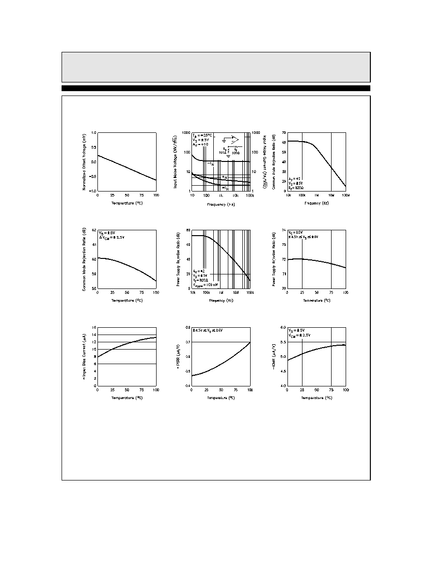
Typical Performance Curves
vs Temperature
Normalized Offset Voltage
Equivalent Input Noise
Ratio vs Frequency
Common Mode Rejection
Ratio vs Temperature
Common Mode Rejection
Ratio vs Frequency
Power Supply Rejection
Ratio vs Temperature
Power Supply Rejection
vs Temperature
b
Input Bias Current
Rejection Ratio
Power Supply
b
Input Bias Current
Ratio vs Temperature
Common Mode Rejection
b
Input Bias Current
2130 ≠ 2
4

EL2130C
85 MHz Current Feedback Amplifier
Typical Performance Curves
Contd
vs Temperature
Supply Current
vs Temperature
a
Input Bias Current
Ratio vs Temperature
Power Supply Rejection
a
Input Bias Current
vs Temperature
Transimpedance (R
OL
)
vs Frequency
Transimpedance (R
OL
)
vs Temperature
Open Loop Gain
Frequency Response
vs Temperature
Output Voltage
vs Temperature
Short Circuit Current
2130 ≠ 3
5