 | –≠–ª–µ–∫—Ç—Ä–æ–Ω–Ω—ã–π –∫–æ–º–ø–æ–Ω–µ–Ω—Ç: EL2160CS | –°–∫–∞—á–∞—Ç—å:  PDF PDF  ZIP ZIP |

EL2160C
December
1995
Rev
B
EL2160C
130 MHz Current Feedback Amplifier
Note All information contained in this data sheet has been carefully checked and is believed to be accurate as of the date of publication however this data sheet cannot be a ``controlled document'' Current revisions if any to these
specifications are maintained at the factory and are available upon your request We recommend checking the revision level before finalization of your design documentation
1993 Elantec Inc
Features
130 MHz 3 dB bandwidth
(A
V
e a
2)
180 MHz 3 dB bandwidth
(A
V
e a
1)
0 01% differential gain
R
L
e
500
X
0 01 differential phase
R
L
e
500
X
Low supply current 8 5 mA
Wide supply range
g
2V to
g
15V
80 mA output current (peak)
Low cost
1500 V ms slew rate
Input common mode range to
within 1 5V of supplies
35 ns settling time to 0 1%
Applications
Video amplifiers
Cable drivers
RGB amplifiers
Test equipment amplifiers
Current to voltage converter
Ordering Information
Part No
Temp Range
Package
Outline
EL2160CN
b
40 C to
a
85 C 8-Pin P-DIP MDP0031
EL2160CS
b
40 C to
a
85 C 8-Pin SOIC
MDP0027
General Description
The EL2160C is a current feedback operational amplifier with
b
3 dB bandwidth of 130 MHz at a gain of
a
2 Built using the
Elantec proprietary monolithic complementary bipolar process
this amplifer uses current mode feedback to achieve more band-
width at a given gain than a conventional voltage feedback op-
erational amplifier
The EL2160C is designed to drive a double terminated 75
X coax
cable to video levels Differential gain and phase are excellent
when driving both loads of 500
X (
k
0 01%
k
0 01 ) and double
terminated 75
X cables (0 025% 0 1 )
The amplifier can operate on any supply voltage from 4V
(
g
2V) to 33V (
g
16 5V) yet consume only 8 5 mA at any sup-
ply voltage Using industry standard pinouts the EL2160C is
available in 8-pin P-DIP and 8-pin SO packages For dual and
quad applications please see the EL2260C EL2460C datasheet
Elantec's facilities comply with MIL-I-45208A and offer appli-
cable quality specifications See the Elantec document QRA-2
Elantec's Military Processing
Monolithic Products
Connection Diagram
EL2160C SO P-DIP
Packages
2060 ≠ 1
Top View

EL2160C
130 MHz Current Feedback Amplifier
Absolute Maximum Ratings
(T
A
e
25 C)
Voltage between V
S
a
and V
S
b
a
33V
Voltage between
a
IN and
b
IN
g
6V
Current into
a
IN or
b
IN
10 mA
Internal Power Dissipation
See Curves
Operating Ambient Temperature Range
b
40 C to
a
85 C
Operating Junction Temperature
Plastic Packages
150 C
Output Current
g
50 mA
Storage Temperature Range
b
65 C to
a
150 C
Important Note
All parameters having Min Max specifications are guaranteed The Test Level column indicates the specific device testing actually
performed during production and Quality inspection Elantec performs most electrical tests using modern high-speed automatic test
equipment specifically the LTX77 Series system Unless otherwise noted all tests are pulsed tests therefore T
J
e
T
C
e
T
A
Test Level
Test Procedure
I
100% production tested and QA sample tested per QA test plan QCX0002
II
100% production tested at T
A
e
25 C and QA sample tested at T
A
e
25 C
T
MAX
and T
MIN
per QA test plan QCX0002
III
QA sample tested per QA test plan QCX0002
IV
Parameter is guaranteed (but not tested) by Design and Characterization Data
V
Parameter is typical value at T
A
e
25 C for information purposes only
Open Loop DC Electrical Characteristics
V
S
e
g
15V R
L
e
150
X T
A
e
25 C unless otherwise specified
Parameter
Description
Conditions
Temp
Limits
Test Level
Units
Min
Typ
Max
EL2160C
V
OS
Input Offset Voltage
V
S
e
g
5V
g
15V
25 C
2
10
I
mV
TC V
OS
Average Offset Voltage
Full
10
V
mV C
Drift (Note 1)
a
I
IN
a
Input Current
V
S
e
g
5V
g
15V
25 C
0 5
5
I
mA
b
I
IN
b
Input Current
V
S
e
g
5V
g
15V
25 C
5
25
I
mA
CMRR
Common Mode Rejection
V
S
e
g
5V
g
15V
25 C
50
55
II
dB
Ratio (Note 2)
b
ICMR
b
Input Current Common
V
S
e
g
5V
g
15V
25 C
0 2
5
I
mA V
Mode Rejection (Note 2)
PSRR
Power Supply Rejection
25 C
75
95
II
dB
Ratio (Note 3)
b
IPSR
b
Input Current Power
25 C
0 2
5
I
mA V
Supply Rejection (Note 3)
2
TD
is
25in

EL2160C
130 MHz Current Feedback Amplifier
Open Loop DC Electrical Characteristics
Contd
V
S
e
g
15V R
L
e
150
X T
A
e
25 C unless otherwise specified
Parameter
Description
Conditions
Temp
Limits
Test Level
Units
Min
Typ
Max
EL2160C
R
OL
Transimpedance
V
S
e
g
15V
25 C
500
2000
I
k
X
(Note 4)
R
L
e
400
X
V
S
e
g
5V
25 C
500
1800
I
k
X
R
L
e
150
X
a
R
IN
a
Input Resistance
25 C
1 5
3 0
II
M
X
a
C
IN
a
Input Capacitance
25 C
2 5
V
pF
CMIR
Common Mode Input Range
V
S
e
g
15V
25 C
g
13 5
V
V
V
S
e
g
5V
25 C
g
3 5
V
V
V
O
Output Voltage Swing
R
L
e
400
X
25 C
g
12
g
13 5
I
V
V
S
e
g
15V
R
L
e
150
X
25 C
g
12
V
V
V
S
e
g
15V
R
L
e
150
X
25 C
g
3 0
g
3 7
I
V
V
S
e
g
5V
I
SC
Output Short Circuit
V
S
e
g
5V
25 C
60
100
150
I
mA
Current (Note 5)
V
S
e
g
15V
I
S
Supply Current
V
S
e
g
15V
25 C
8 5
12 0
I
mA
V
S
e
g
5V
25 C
6 4
9 5
I
mA
3
TD
is
34in

EL2160C
130 MHz Current Feedback Amplifier
Closed Loop AC Electrical Characteristics
V
S
e
g
15V A
V
e a
2 R
F
e
560
X R
L
e
150
X T
A
e
25 C unless otherwise noted
Parameter
Description
Conditions
Limits
Test Level
Units
Min
Typ
Max
EL2160C
BW
b
3 dB Bandwidth
V
S
e
g
15V A
V
e a
2
130
V
MHz
(Note 8)
V
S
e
g
15V A
V
e a
1
180
V
MHz
V
S
e
g
5V A
V
e a
2
100
V
MHz
V
S
e
g
5V A
V
e a
1
110
V
MHz
SR
Slew Rate
R
L
e
400
X
1000
1500
IV
V
ms
(Notes 6 8)
R
F
e
1K
X R
G
e
110
X
1500
V
V
ms
R
L
e
400
X
t
r
t
f
Rise Time
V
OUT
e
g
500mV
2 7
V
ns
Fall Time (Note 8)
t
pd
Propagation Delay
3 2
V
ns
(Note 8)
OS
Overshoot (Note 8)
V
OUT
e
g
500 mV
0
V
%
t
s
0 1% Settling Time
V
OUT
e
g
10V
35
V
ns
(Note 8)
A
V
e b
1 R
L
e
1K
dG
Differential Gain
R
L
e
150
X
0 025
V
%
(Notes 7 8)
R
L
e
500
X
0 006
V
%
dP
Differential Phase
R
L
e
150
X
0 1
V
deg ( )
(Notes 7 8)
R
L
e
500
X
0 005
V
deg ( )
Note 1 Measured from T
MIN
to T
MAX
Note 2 V
CM
e
g
10V for V
S
e
g
15V and T
A
e
25 C
V
CM
e
g
3V for V
S
e
g
5V and T
A
e
25 C
Note 3 The supplies are moved from
g
2 5V to
g
15V
Note 4 V
OUT
e
g
7V for V
S
e
g
15V and V
OUT
e
g
2V for V
S
e
g
5V
Note 5 A heat sink is required to keep junction temperature below absolute maximum when an output is shorted
Note 6 Slew Rate is with V
OUT
from
a
10V to
b
10V and measured at the 25% and 75% points
Note 7 DC offset from
b
0 714V through
a
0 714V AC amplitude 286 mV
p-p
f
e
3 58 MHz
Note 8 All AC tests are performed on a ``warmed up'' part except for Slew Rate which is pulse tested
4
TD
is
35in
EL2160C
130 MHz Current Feedback Amplifier
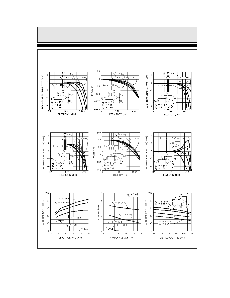
Typical Performance Curves
Response (Gain)
Non-Inverting Frequency
Response (Phase)
Non-Inverting Frequency
for Various R
L
Frequency Response
Response (Gain)
Inverting Frequency
Response (Phase)
Inverting Frequency
Various R
F
and R
G
Frequency Response for
Voltage for A
V
e
b
1
3 dB Bandwidth vs Supply
for A
V
e
b
1
Peaking vs Supply Voltage
Temperature for A
V
e
b
1
3 dB Bandwidth vs
2060 ≠ 2
5