 | –≠–ª–µ–∫—Ç—Ä–æ–Ω–Ω—ã–π –∫–æ–º–ø–æ–Ω–µ–Ω—Ç: EL2221CN | –°–∫–∞—á–∞—Ç—å:  PDF PDF  ZIP ZIP |

Note: All information contained in this data sheet has been carefully checked and is believed to be accurate as of the date of publication; however, this data sheet cannot be a "controlled document". Current revisions, if any, to these
specifications are maintained at the factory and are available upon your request. We recommend checking the revision level before finalization of your design documentation.
© 1997 Elantec, Inc.
EL
2221C
General Description
The EL2221C operational amplifier, built using Elantec's comple-
mentary bipolar process, offers unprecedented high frequency
performance at a very low cost. It is suitable for any application, such
as consumer video, where traditional DC performance specifications
are of secondary importance to the high frequency specifications. On a
5V supply at a gain of +2 the EL2221C will drive a 150
load to +2V,
with a bandwidth of 100 MHz . This device achieves 0.1 dB band-
width at 5 MHz.
The recommended power supply voltage is 5V. At zero and 5V sup-
plies, the inputs will operate to ground. When the outputs are at 0V the
amplifier draws only 2.4 mA of supply current.
Connection Diagram
P-DIP, SO
Features
∑
Optimized for 5V operation
∑
Stable at gain of 2
∑
100 MHz Gain bandwidth product
∑
130 V/µs slew rate
∑
Drives 150
load to video levels
∑
Input and outputs operate at
negative supply rail
∑
-60 dB isolation at 4.2 MHz
Applications
∑
Consumer video amplifier
∑
Active filters/integrators
∑
Cost sensitive applications
∑
Single supply amplifiers
Ordering Information
Part No
Temp. Range
Package
Outline #
EL2221CN
-40∞C to +85∞C
8-lead P-DIP
MDP0031
EL2221CS
-40∞C to +85∞C
8-lead SO
MDP0027
EL2221C
Dual, Low Cost, Gain of 2, Video Op Amp
Fe
b
r
u
a
r
y
19
97 R
e
v A
2
EL2221C
Dual, Low Cost, Gain of 2, Video Op Amp
E
L
2221C
Absolute Maximum Ratings
(T
A
= 25 ∞C)
Total Supply Voltage
18V
Input Voltage
-6V
S
Differential Input Voltage
6V
Peak Output Current
75 mA per amplifier
Power Dissipation
See Curves
Storage Temperature Range
-65∞C to +150∞C
Operating Temperature Range
-40∞C to +85∞C
1.
Measured from T
MIN
to T
MAX
.
2.
A heat-sink is required to keep junction temperature below absolute maximum when an output is shorted.
Important Note:
All parameters having Min/Max specifications are guaranteed. The Test Level column indicates the specific device testing actually performed during
production and Quality inspection. Elantec performs most electrical tests using modern high-speed automatic test equipment, specifically the LTX77
Series system. Unless otherwise noted, all tests are pulsed tests, therefor T
J
= T
C
= T
A
.
Test Level
Test Procedure
I
100% production tested and QA sample tested per QA test plan QCX0002.
II
100% production tested at T
A
= 25∞C and QA sample tested at T
A
= 25∞C, T
MAX
and T
MIN
per QA test plan QCX0002.
III
QA sample tested per QA test plan QCX0002.
IV
Parameter is guaranteed (but not tested) by Design and Characterization Data.
V
Parameter is typical value at T
A
= 25∞C for information purposes only.
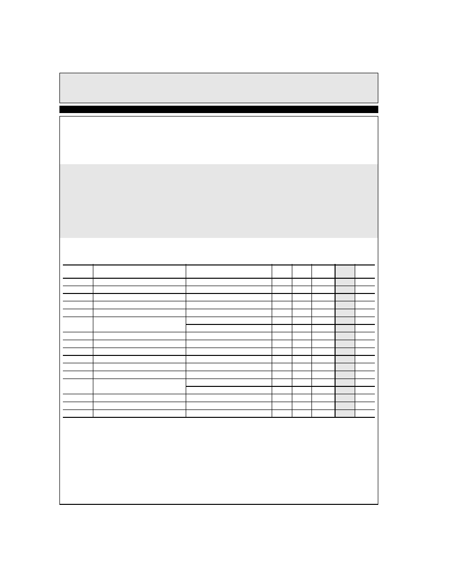
DC Characteristics
V
S
=+5V, R
L
=1K
, V
IN
=1V, T
A
=25∞C unless otherwise specified.
Parameter
Description
Conditions
Min
Typ
Max
Test
Level
Units
V
OS
Input Offset Voltage
-20
10
20
I
mV
TCV
OS
Average Offset Voltage Drift
[1]
-50
V
µ V/∞C
I
B
Input Bias Current
-15
-7
-3
I
µA
I
OS
Input Offset Current
0.3
1.0
I
µA
TCI
OS
Average Offset Current Drift
[1]
-1
-3
V
nA/∞C
A
VOL
Open Loop Gain
V
OUT=.
.5, 2.5, R
L
= 1K
160
250
I
V/V
V
OUT=.
.5, 2.5, R
L
= 150K
160
250
V
V/V
PSRR
Power Supply Rejection Ratio
V
S
= 4.5V to 5.5V
43
50
I
dB
CMRR
Common Mode Rejection Ratio
VCM = 0V to +3.8V
60
65
I
dB
CMIR
Common Mode Input Range
0.0
3.0
I
V
V
OUT
Output Voltage Swing
RFB = R
G
= 1K, R
L
= 150
2.8
3.2
I
V
I
SC
Output Short Circuit Current
Output to Ground
[2]
75
125
I
mA
I
S
Supply Current
No Load (per channel) V
IN
= 0V
2.0
2.4
3.0
I
mA
R
IN
Input Resistance
Differential
150
V
K
Common Mode
1.5
V
M
C
IN
Input Capacitance
A
V
= +1 @ 10 MHz
1
V
pF
R
OUT
Output Resistance
0.150
V
PSOR
Power Supply Operating Range
Single Supply
4
6
V
V

3
EL2221C
Dual, Low Cost, Gain of 2, Video Op Amp
EL
2221C
1.
For V
S
= 5V, V
OUT
= 4V
pp
. Full power bandwidth is based on slew rate measurement using: FPBW = SR/(2pi*V
peak
)
2.
Video performance measured at V
S
= 5V, A
V
= +2 with 2 times normal video level across R
L
= 150
Closed Loop AC Electrical Characteristics
V
S
=5V, AC Test Figure, T
A
= 25∞C unless otherwise specified
Parameter
Description
Conditions
Min
Typ
Max
Test
Level
Units
BW
-3dB Bandwidth (V
OUT
= 0.4 mVp-p)
±0.1 dB Bandwidth (V
OUT
= 0.4 mVp-p)
A
V
= +1
100
V
MHz
A
V
= +1
10
V
MHz
GBWP
Gain Bandwidth Product
50
V
MHz
PM
Phase Margin
55
V
( ∞ )
SR
Slew Rate
85
130
V
V/µs
FBWP
Full Power Bandwidth
[1]
8
11
V
MHz
t
R
, t
F
Rise Time, Fall Time
0.1V step
2
V
ns
OS
Overshoot
0.1V step
15
V
%
t
PD
Propagation Delay
3.5
V
ns
t
S
Settling to 0.1% (A
V
= 1)
VS = 5V, 2V Step
80
V
ns
dG
Differential Gain
[2]
NTSC/PAL
0.1
V
%
dP
Differential Phase
[2]
NTSC/PAL
0.2
V
( ∞ )
e
N
Input Noise Voltage
10 KHz
15
V
nV/rt(Hz)
i
N
Input Noise Current
10 KHz
1.5
V
nV/rt(Hz)
CS
Channel Separation
P = 5 MHz
55
V
dB
4
EL2221C
Dual, Low Cost, Gain of 2, Video Op Amp
E
L
2221C
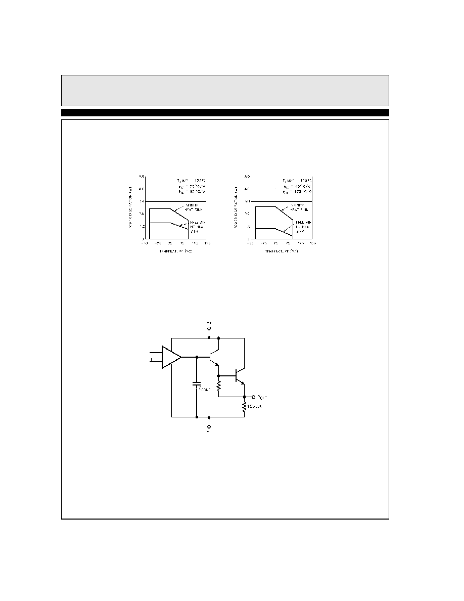
Typical Performance Curves
Simplified Block Diagram
8-Pin Plastic DIP
Maximum Power Dissipation
vs Ambient Temperature
8-Lead SO
Maximum Power Dissipation
vs Ambient Temperature

5
EL2221C
Dual, Low Cost, Gain of 2, Video Op Amp
EL
2221C
Applications Information
Product Description
The EL2221C operational amplifier is stable at a gain of
1. It is built on Elantec's proprietary complimentary
bipolar process. This topology allows it to be used in a
variety of applications where current mode amplifiers
are not appropriate because of restrictions placed on the
feedback elements. This product is especially designed
for applications where high bandwidth and good video
performance characteristics are desired but the higher
cost of more flexible and sophisticated products are
prohibitive.
Power Supplies
The EL2221C is designed to work at a supply voltage
difference of 4.5V to 5.5V. It will work on any combina-
tion of ± supplies. All electrical characteristics are
measured with a 5V supply.
Output Swing vs Load
Please refer to the simplified block diagram. This ampli-
fier provides an NPN pull-up transistor output and a
passive 1250
pull-down resistor to the most negative
supply. In a application where the load is connected to
V
S
-
the output voltage can swing to within 200 mV of
V
S
- .
Output Drive Capability
This device does not have short circuit protection. Each
output is capable of than 100 mA into a shorted output.
Care must be used in the design to limit the output cur-
rent with a series resistor.
Single 5 Volt Supply Video Cable Driver
These amplifiers may be used as a direct coupled video
cable driver with a gain of 2. With a 75
back matching
resistor driving a terminated 75
cable the output at the
cable load will be original video level (1V NTSC). The
best operating mode is with direct coupling. The input
signal must be offset to keep the entire signal within the
range of the amplifier. The required offset voltage can
be set with a resistor divider and a bypass capacitor in
the video path (Figure 1). The input DC offset should be
between.3V and .5V. With R
A
=68K and R
B
=4.7K the
input offset will be .32V. Since these amplifiers require
a DC load at their outputs it is good design practice to
add a 250
resistor to ground directly at the amplifier
output. Then if the 75
cable termination resistor were
inadvertently removed there would still be an output sig-
nal. The values in figure 1 give an output range of 0V to
2.6V
Output capacitive coupling also has some restrictions.
These amplifiers require a DC load at their outputs. A
75
back matching resistor to a cable and a 75
load to
ground at the end of the cable provide a 150
DC load.
But output capacitive coupling opens this DC path so an
extra pulldown resistor on the amplifier output to ground
is required. Figure 4 shows a 250
resistor. Capacitively
coupling the output will require that we shift the output
offset voltage higher than in the direct coupled case.
Using R
A
=43K and R
B
=4.7K will make the quiescent
output offset voltage about 1V. The output dynamic
range will be .6V to 3V.