
Note: All information contained in this data sheet has been carefully checked and is believed to be accurate as of the date of publication; however, this data sheet cannot be a "controlled document". Current revisions, if any, to these
specifications are maintained at the factory and are available upon your request. We recommend checking the revision level before finalization of your design documentation.
© 2001 Elantec Semiconductor, Inc.
E
L
2
2
2
7
C
General Description
The EL2227C is a dual, low-noise amplifier, ideally suited to line
receiving applications in ADSL and HDSLII designs. With low noise
specification of just 1.9nV/
Hz and 1.2pA/
Hz, the EL2227C is per-
fect for the detection of very low amplitude signals.
The EL2227C features a -3dB bandwidth of 115MHz and is gain-of-2
stable. The EL2227C also affords minimal power dissipation with a
supply current of just 4.8mA per amplifier. The amplifier can be pow-
ered from supplies ranging from ±2.5V to ±12V.
The EL2227C is available in a space-saving 8-pin MSOP package as
well as the industry-standard 8-pin SO. It can operate over the -40∞C
to +85∞C temperature range.
Connection Diagram
1
2
3
4
8
7
6
5
-
+
-
+
VS-
VS+
VINA+
VINA-
VOUTA
VOUTB
VINB-
VINB+
EL2227C
(8-Pin SO and 8-Pin MSOP)
Features
∑ Voltage noise of only 1.9nV/
Hz
∑ Current noise of only 1.2pA/
Hz
∑ Bandwidth (-3dB) of 115MHz
@A
V
= +2
∑ Gain-of-2 stable
∑ Just 4.8mA per amplifier
∑ 8-pin MSOP package
∑ ±2.5V to ±12V operation
Applications
∑ ADSL receivers
∑ HDSLII receivers
∑ Ultrasound input amplifiers
∑ Wideband instrumentation
∑ Communications equipment
∑ AGC & PLL active filters
∑ Wideband sensors
Ordering Information
Part No.
Package
Tape & Reel
Outline #
EL2227CY
8-Pin MSOP
-
MDP0043
EL2227CY-T13
8-Pin MSOP
13"
MDP0043
EL2227CY-T7
8-Pin MSOP
7"
MDP0043
EL2227CS
8-Pin SO
-
MDP0027
EL2227CS-T13
8-Pin SO
13"
MDP0027
EL2227CS-T7
8-Pin SO
7"
MDP0027
EL2227C
Dual Very Low Noise Amplifier
A
u
g
u
s
t
3
,
2
0
0
1

2
EL2227C
Dual Very Low Noise Amplifier
E
L
2
2
2
7
C
Absolute Maximum Ratings
(T
A
= 25∞C)
Values beyond absolute maximum ratings can cause the device to be pre-
maturely damaged. Absolute maximum ratings are stress ratings only
and functional device operation is not implied
Supply Voltage between V
S
+ and V
S
-
28V
Input Voltage
V
S
- - 0.3V, V
S
+0.3V
Maximum Continuous Output Current
40mA
Maximum Die Temperature
150∞C
Storage Temperature
-65∞C to +150∞C
Operating Temperature
-40∞C to +85∞C
Power Dissipation
See Curves
ESD Voltage
2kV
Important Note:
All parameters having Min/Max specifications are guaranteed. Typ values are for information purposes only. Unless otherwise noted, all tests are at the
specified temperature and are pulsed tests, therefore: T
J
= T
C
= T
A
.
Electrical Characteristics
V
S
+ = +12V, V
S
- = -12V, R
L
= 500
and C
L
= 3pF to 0V, R
F
= R
G
= 620
, and T
A
= 25∞C unless otherwise specified.
Parameter
Description
Condition
Min
Typ
Max
Unit
Input Characteristics
V
OS
Input Offset Voltage
V
CM
= 0V
-0.2
3
mV
TCV
OS
Average Offset Voltage Drift
[1]
-0.6
µV/∞C
I
B
Input Bias Current
V
CM
= 0V
-9
-3.4
µA
R
IN
Input Impedance
7.3
M
C
IN
Input Capacitance
1.6
pF
CMIR
Common-Mode Input Range
-11.8
+10.4
V
CMRR
Common-Mode Rejection Ratio
for V
IN
from -11.8V to 10.4V
60
94
dB
A
VOL
Open-Loop Gain
-5V
V
OUT
5V
70
87
dB
e
n
Voltage Noise
f = 100kHz
1.9
nV/
Hz
i
n
Current Noise
f = 100kHz
1.2
pA/
Hz
Output Characteristics
V
OL
Output Swing Low
R
L
= 500
-10.4
-10
V
R
L
= 250
-9.8
-9
V
V
OH
Output Swing High
R
L
= 500
10
10.4
V
R
L
= 250
9.5
10
V
I
SC
Short Circuit Current
R
L
= 10
140
180
mA
Power Supply Performance
PSRR
Power Supply Rejection Ratio
V
S
is moved from ±2.25V to ±12V
65
95
dB
I
S
Supply Current (Per Amplifier)
No Load
4.8
6.5
mA
V
S
Operating Range
±2.5
±12
V
Dynamic Performance
SR
Slew Rate
[2]
±2.5V square wave, measured 25%-75%
40
50
V/µS
t
S
Settling to 0.1% (A
V
= +2)
(A
V
= +2), V
O =
±1V
65
ns
BW
-3dB Bandwidth
R
F
= 358
115
MHz
HD2
2nd Harmonic Distortion
f = 1MHz, V
O
= 2V
P-P
, R
L
= 500
, R
F
= 358
93
dBc
f = 1MHz, V
O
= 2V
P-P
, R
L
= 150
, R
F
= 358
83
dBc
HD3
3rd Harmonic Distortion
f = 1MHz, V
O
= 2V
P-P
, R
L
= 500
, R
F
= 358
94
dBc
f = 1MHz, V
O
= 2V
P-P
, R
L
= 150
, R
F
= 358
76
dBc

3
EL2227C
Dual Very Low Noise Amplifier
E
L
2
2
2
7
C
Electrical Characteristics
V
S
+= +5V, V
S
- = -5V, R
L
= 500
and C
L
= 3pF to 0V, R
F
= 620
& T
A
= 25∞C unless otherwise specified.
Parameter
Description
Condition
Min
Typ
Max
Unit
Input Characteristics
V
OS
Input Offset Voltage
V
CM
= 0V
0.2
3
mV
TCV
OS
Average Offset Voltage Drift
[1]
-0.6
µV/∞C
I
B
Input Bias Current
V
CM
= 0V
-9
-3.7
µA
R
IN
Input Impedance
7.3
M
C
IN
Input Capacitance
1.6
pF
CMIR
Common-Mode Input Range
-4.8
3.4
V
CMRR
Common-Mode Rejection Ratio
for V
IN
from -4.8V to 3.4V
60
97
dB
A
VOL
Open-Loop Gain
-5V
V
OUT
5V
70
84
dB
e
n
Voltage Noise
f = 100kHz
1.9
nV/
Hz
i
n
Current Noise
f = 100kHz
1.2
pA/
Hz
Output Characteristics
V
OL
Output Swing Low
R
L
= 500
-3.8
-3.5
V
R
L
= 250
-3.7
-3.5
V
V
OH
Output Swing High
R
L
= 500
3.5
3.7
V
R
L
= 250
3.5
3.6
V
I
SC
Short Circuit Current
R
L
= 10
60
100
mA
Power Supply Performance
PSRR
Power Supply Rejection Ratio
V
S
is moved from ±2.25V to ±12V
65
95
dB
I
S
Supply Current (Per Amplifier)
No Load
4.5
5.5
mA
V
S
Operating Range
±2.5
±12
V
Dynamic Performance
SR
Slew Rate
[2]
±2.5V square wave, measured 25%-75%
35
45
V/µS
t
S
Settling to 0.1% (A
V
= +2)
(A
V
= +2), V
O =
±1V
77
ns
BW
-3dB Bandwidth
R
F
= 358
90
MHz
HD2
2nd Harmonic Distortion
f = 1MHz, V
O
= 2V
P-P
, R
L
= 500
, R
F
= 358
98
dBc
f = 1MHz, V
O
= 2V
P-P
, R
L
= 150
, R
F
= 358
90
dBc
HD3
3rd Harmonic Distortion
f = 1MHz, V
O
= 2V
P-P
, R
L
= 500
, R
F
= 358
94
dBc
f = 1MHz, V
O
= 2V
P-P
, R
L
= 150
, R
F
= 358
79
dBc

4
EL2227C
Dual Very Low Noise Amplifier
E
L
2
2
2
7
C
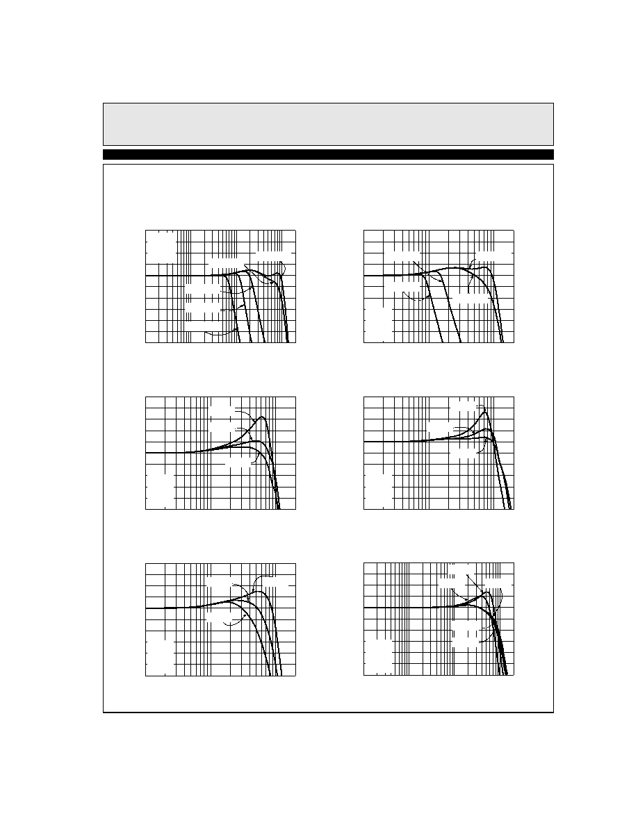
Typical Performance Curves
Non-inverting Frequency Response for Various R
F
4
3
2
1
0
-1
-2
-3
-4
-5
-6
1M
10M
100M
Frequency (Hz)
N
o
r
m
a
l
i
z
e
d
G
a
i
n
(
d
B
)
200M
V
S
=±12V
A
V
=+2
R
L
=500
R
F
=620
R
F
=350
R
F
=100
R
F
=1k
Inverting Frequency Response for Various R
F
4
3
2
1
0
-1
-2
-3
-4
-5
-6
1M
10M
100M
Frequency (Hz)
N
o
r
m
a
l
i
z
e
d
G
a
i
n
(
d
B
)
200M
V
S
=±12V
A
V
=-1
R
L
=500
Inverting Frequency Response (Gain)
4
3
2
1
0
-1
-2
-3
-4
-5
-6
1M
10M
100M
Frequency (Hz)
N
o
r
m
a
l
i
z
e
d
G
a
i
n
(
d
B
)
200M
V
S
=±12V
R
F
=420
R
L
=500
Non-inverting Frequency Response (Gain)
4
3
2
1
0
-1
-2
-3
-4
-5
-6
1M
10M
100M
Frequency (Hz)
N
o
r
m
a
l
i
z
e
d
G
a
i
n
(
d
B
)
200M
Inverting Frequency Response (Phase)
135
90
45
0
-45
-90
-135
-180
-225
-270
-315
1M
10M
100M
Frequency (Hz)
P
h
a
s
e
(
∞
)
200M
V
S
=±12V
R
F
=420
R
L
=500
R
F
=420
R
F
=350
R
F
=100
R
F
=1k
R
F
=620
V
S
=±12V
R
F
=350
R
L
=500
A
V
=2
A
V
=5
A
V
=10
A
V
=-10
A
V
=-5
A
V
=-2
A
V
=-1
A
V
=-10
A
V
=-5
A
V
=-2
A
V
=-1
Non-inverting Frequency Response (Phase)
135
90
45
0
-45
-90
-135
-180
-225
-270
-315
1M
10M
Frequency (Hz)
P
h
a
s
e
(
∞
)
100M 200M
V
S
=±12
R
F
=350
R
L
=500
A
V
=10
A
V
=2
A
V
=5
5
EL2227C
Dual Very Low Noise Amplifier
E
L
2
2
2
7
C
Typical Performance Curves
Non-inverting Frequency Response for Various
Input Signal Levels
4
3
2
1
0
-1
-2
-3
-4
-5
-6
100k
1M
10M
Frequency (Hz)
N
o
r
m
a
l
i
z
e
d
G
a
i
n
(
d
B
)
100M
V
S
=±12V
R
F
=350
A
V
=+2
R
L
=500
V
IN
=500mV
PP
V
IN
=100mV
PP
V
IN
=20mV
PP
V
IN
=1V
PP
V
IN
=2V
PP
Inverting Frequency Response for Various Input
Signal Levels
4
3
2
1
0
-1
-2
-3
-4
-5
-6
1M
10M
100M
Frequency (Hz)
N
o
r
m
a
l
i
z
e
d
G
a
i
n
(
d
B
)
200M
Non-inverting Frequency Response for Various R
L
4
3
2
1
0
-1
-2
-3
-4
-5
-6
1M
10M
100M
Frequency (Hz)
N
o
r
m
a
l
i
z
e
d
G
a
i
n
(
d
B
)
200M
Inverting Frequency Response for Various C
L
4
3
2
1
0
-1
-2
-3
-4
-5
-6
1M
10M
100M
Frequency (Hz)
N
o
r
m
a
l
i
z
e
d
G
a
i
n
(
d
B
)
200M
Non-inverting Frequency Response for Various C
L
5
4
3
2
1
0
-1
-2
-3
-4
-5
1M
10M
100M
Frequency (Hz)
N
o
r
m
a
l
i
z
e
d
G
a
i
n
(
d
B
)
200M
R
L
=50
R
L
=100
R
L
=500
V
S
=±12V
R
F
=620
R
L
=500
A
V
=+2
V
S
=±12V
R
F
=420
R
L
=500
A
V
=-1
V
IN
=20mV
PP
V
IN
=280mV
PP
V
IN
=1.4V
PP
V
IN
=2.8V
PP
V
S
=±12V
R
F
=620
C
L
=15pF
A
V
=+2
C
L
=30pF
C
L
=12pF
C
L
=2pF
V
S
=±12V
R
F
=420
R
L
=500
A
V
=-1
C
L
=30pF
C
L
=12pF
C
L
=2pF
Frequency Response for Various Output DC
Levels
4
3
2
1
0
-1
-2
-3
-4
-5
-6
100k
1M
10M
Frequency (Hz)
N
o
r
m
a
l
i
z
e
d
G
a
i
n
(
d
B
)
V
S
=±12V
R
F
=620
R
L
=500
A
V
=+2
V
O
=+10V
V
O
=-10V
V
O
=+5V
V
O
=0V
V
O
=-5V
100M