 | –≠–ª–µ–∫—Ç—Ä–æ–Ω–Ω—ã–π –∫–æ–º–ø–æ–Ω–µ–Ω—Ç: EL2480C | –°–∫–∞—á–∞—Ç—å:  PDF PDF  ZIP ZIP |

Note: All information contained in this data sheet has been carefully checked and is believed to be accurate as of the date of publication; however, this data sheet cannot be a "controlled document". Current revisions, if any, to these
specifications are maintained at the factory and are available upon your request. We recommend checking the revision level before finalization of your design documentation.
© 2001 Elantec Semiconductor, Inc.
E
L
2
1
8
0
C
/
E
L
2
2
8
0
C
/
E
L
2
4
8
0
C
-
General Description
The EL2180C/EL2280C/EL2480C are single/dual/quad current-feed-
back operational amplifiers that achieve a -3dB bandwidth of 250MHz
at a gain of +1 while consuming only 3mA of supply current per
amplifier. They will operate with dual supplies ranging from ±1.5V to
±6V or from single supplies ranging from +3V to +12V. In spite of
their low supply current, the EL2480C and the EL2280C can output
55mA while swinging to ±4V on ±5V supplies. The EL2180C can out-
put 100mA with similar output swings. These attributes make the
EL2180C/EL2280C/EL2480C excellent choices for low power and/or
low voltage cable driver, HDSL, or RGB applications.
For applications where board space is extremely critical, the EL2180C
is available in the tiny 5-pin SOT23 package, with a footprint size 28%
of an 8-pin SO. The EL2480C is also available in a 24-pin LPP pack-
age. All are specified for operation over the full -40∞C to +85∞C
temperature range.
Single, dual, and triple versions are also available with the enable
function (EL2186C, EL2286C, and EL2386C).
Connection Diagrams
1
2
3
4
8
7
6
5
EL2180C
(8-Pin SO & 8-Pin PDIP)
-
+
NC
IN-
IN+
VS-
NC
VS+
OUT
NC
1
2
3
4
8
7
6
5
EL2280C
(8-Pin SO & 8-Pin PDIP)
-
+
OUTA
INA-
INA+
VS-
VS+
OUTB
INB-
INB+
-
+
A
B
Features
∑ Single, dual, and quad topologies
∑ 3mA supply current (per amplifier)
∑ 250MHz -3dB bandwidth
∑ 1200V/µs slew rate
∑ Tiny package package options
(SOT23, LPP)
∑ Low cost
∑ Single- and dual-supply operation
down to ±1.5V
∑ 0.05%/0.05∞ diff. gain/diff. phase
into 150
Applications
∑ Low power/battery applications
∑ HDSL amplifiers
∑ Video amplifiers
∑ Cable drivers
∑ RGB amplifiers
∑ Test equipment amplifiers
∑ Current to voltage converters
Ordering Information
Part No
Package
Tape &
Reel
Outline #
EL2180CN
8-Pin PDIP
-
MDP0031
EL2180CS
8-Pin SO
-
MDP0027
EL2180CS-T7
8-Pin SO
7"
MDP0027
EL2180CS-T13
8-Pin SO
13"
MDP0027
EL2180CW-T7
5-Pin SOT23
7"
MDP0038
EL2180CW-T13
5-Pin SOT23
13"
MDP0038
EL2280CN
8-Pin PDIP
-
MDP0031
EL2280CS
8-Pin SO
-
MDP0027
EL2280CS-T7
8-Pin SO
7"
MDP0027
EL2280CS-T13
8-Pin SO
13"
MDP0027
EL2480CN
14-Pin PDIP
-
MDP0031
EL2480CS
14-Pin SO
-
MDP0027
EL2480CS-T7
14-Pin SO
7"
MDP0027
EL2480CS-T13
14-Pin SO
13"
MDP0027
EL2480CL
24-Pin LPP
-
MDP0046
EL2480CL-T7
24-Pin LPP
7"
MDP0046
EL2480CL-T13
24-Pin LPP
13"
MDP0046
EL2180C/EL2280C/EL2480C-Preliminary
250MHz / 3mA Current Mode Feedback Amplifiers
J
u
l
y
1
9
,
2
0
0
1

2
EL2180C/EL2280C/EL2480C-Preliminary
250MHz / 3mA Current Mode Feedback Amplifiers
E
L
2
1
8
0
C
/
E
L
2
2
8
0
C
/
E
L
2
4
8
0
C
-
P
r
e
l
i
m
i
n
a
r
y
Absolute Maximum Ratings
(T
A
= 25∞C)
Supply Voltage between V
S
+ and GND
+12.6V
Voltage between V
S
+ and V
S
-
+12.6V
Common-Mode Input Voltage
V
S
- to V
S
+
Differential Input Voltage
±6V
Current into +IN or -IN
±7.5mA
Internal Power Dissipation
See Curves
Operating Ambient Temperature Range
-40∞C to +85∞C
Operating Junction Temperature
Plastic Packages
150∞C
Output Current (EL2180C)
±120mA
Output Current (EL2280C)
±60mA
Output Current (EL2480C)
±60mA
Storage Temperature Range
-65∞C to +150∞C
DC Electrical Characteristics
V
S
= ±5V, R
L
= 150
, T
A
= 25∞C unless otherwise specified.
Parameter
Description
Conditions
Min
Typ
Max
Unit
V
OS
Input Offset Voltage
2.5
10
mV
TCV
OS
Average Input Offset Voltage Drift
Measured from T
MIN
to T
MAX
5
µV/∞C
dV
OS
V
OS
Matching
EL2280C, EL2480C only
0.5
mV
+I
IN
+Input Current
1.5
15
µA
d+I
IN
+I
IN
Matching
EL2280C, EL2480C only
20
nA
-I
IN
-Input Current
16
40
µA
d-I
IN
-I
IN
Matching
EL2280C, EL2480C only
2
µA
CMRR
Common Mode Rejection Ratio
V
CM
= ±3.5V
45
50
dB
-ICMR
-Input Current Common Mode Rejection
V
CM
= ±3.5V
5
30
µA/V
PSRR
Power Supply Rejection Ratio
V
S
is moved from ±4V to ±6V
60
70
dB
-IPSR
-Input Current Power Supply Rejection
V
S
is moved from ±4V to ±6V
1
15
µA/V
R
OL
Transimpedance
V
OUT
= ±2.5V
120
300
k
+R
IN
+Input Resistance
V
CM
= ±3.5V
0.5
2
M
+C
IN
+Input Capacitance
1.2
pF
CMIR
Common Mode Input Range
±3.5
±4.0
V
V
O
Output Voltage Swing
V
S
= ±5
±3.5
±4.0
V
V
S
= +5 Single-supply, high
4.0
V
V
S
= +5 Single-supply, low
0.3
V
I
O
Output Current
EL2180C only
80
100
mA
EL2280C only, per amplifier
50
55
mA
EL2480C only, per amplifier
50
55
mA
I
S
Supply Current
Per amplifier
3
6
mA
Important Note:
All parameters having Min/Max specifications are guaranteed. Typ values are for information purposes only. Unless otherwise noted, all tests are at the
specified temperature and are pulsed tests, therefore: T
J
= T
C
= T
A
.
AC Electrical Characteristics
V
S
= ±5V, R
F
= R
G
= 750
for PDIP and SO packages, R
F
= R
G
= 560
for SOT23-5 package, R
L
= 150
, T
A
= 25∞C unless otherwise specified
Parameter
Description
Conditions
Min
Typ
Max
Unit
-3dB BW
-3dB Bandwidth
A
V
= +1
250
MHz
-3dB BW
-3dB Bandwidth
A
V
= +2
180
MHz
0.1dB BW
0.1dB Bandwidth
A
V
= +2
50
MHz
SR
Slew Rate
V
OUT
= ±2.5V, A
V
= +2
600
1200
V/µs
t
R
, t
F
Rise and Fall Time
V
OUT
= ±500 mV
1.5
ns

3
EL2180C/EL2280C/EL2480C-Preliminary
250MHz / 3mA Current Mode Feedback Amplifiers
E
L
2
1
8
0
C
/
E
L
2
2
8
0
C
/
E
L
2
4
8
0
C
-
P
r
e
l
i
m
i
n
a
r
y
Connection Diagrams (Continued)
t
PD
Propagation Delay
V
OUT
= ±500 mV
1.5
ns
OS
Overshoot
V
OUT
= ±500 mV
3.0
%
t
S
0.1% Settling
V
OUT
= ±2.5V, A
V
= -1
15
ns
dG
Differential Gain
A
V
= +2, R
L
= 150
[1]
0.05
%
dP
Differential Phase
A
V
= +2, R
L
= 150
[1]
0.05
∞
dG
Differential Gain
A
V
= +1, R
L
= 500
[1]
0.01
%
dP
Differential Phase
A
V
= +1, R
L
= 500
[1]
0.01
∞
C
S
Channel Separation
EL2280C, EL2480C only, f = 5 MHz
85
dB
1. DC offset from 0V to 0.714V, AC amplitude 286mV
P-P
, f = 3.58MHz
AC Electrical Characteristics
V
S
= ±5V, R
F
= R
G
= 750
for PDIP and SO packages, R
F
= R
G
= 560
for SOT23-5 package, R
L
= 150
, T
A
= 25∞C unless otherwise specified
Parameter
Description
Conditions
Min
Typ
Max
Unit
1
2
3
4
14
13
12
11
5
6
7
10
9
8
EL2480C
(14-Pin SO & 14-Pin PDIP)
19
18
17
16
15
14
13
2
4
2
3
2
2
2
1
2
0
8
9
1
0
1
1
1
2
1
2
3
4
5
6
7
EL2480C
(24-Pin LPP - Top View)
Thermal Pad
NC
INA+
NC
VS+
NC
INB+
NC
NC
IND+
NC
VS-
NC
INC+
NC
I
N
A
-
O
U
T
A
N
C
O
U
T
D
I
N
D
-
I
N
B
-
O
U
T
B
N
C
O
U
T
C
I
N
C
-
1
2
3
5
4
EL2180C
(5-Pin SOT23)
OUT
GND
IN+
VS+
IN-
-
+
OUTA
INA-
INA+
VS+
OUTD
IND-
IND+
VS-
INB+
INB-
OUTB
INC+
INC-
OUTC
- +
-
+
- +
-
+
B
C
A
D
4
EL2180C/EL2280C/EL2480C-Preliminary
250MHz / 3mA Current Mode Feedback Amplifiers
E
L
2
1
8
0
C
/
E
L
2
2
8
0
C
/
E
L
2
4
8
0
C
-
P
r
e
l
i
m
i
n
a
r
y
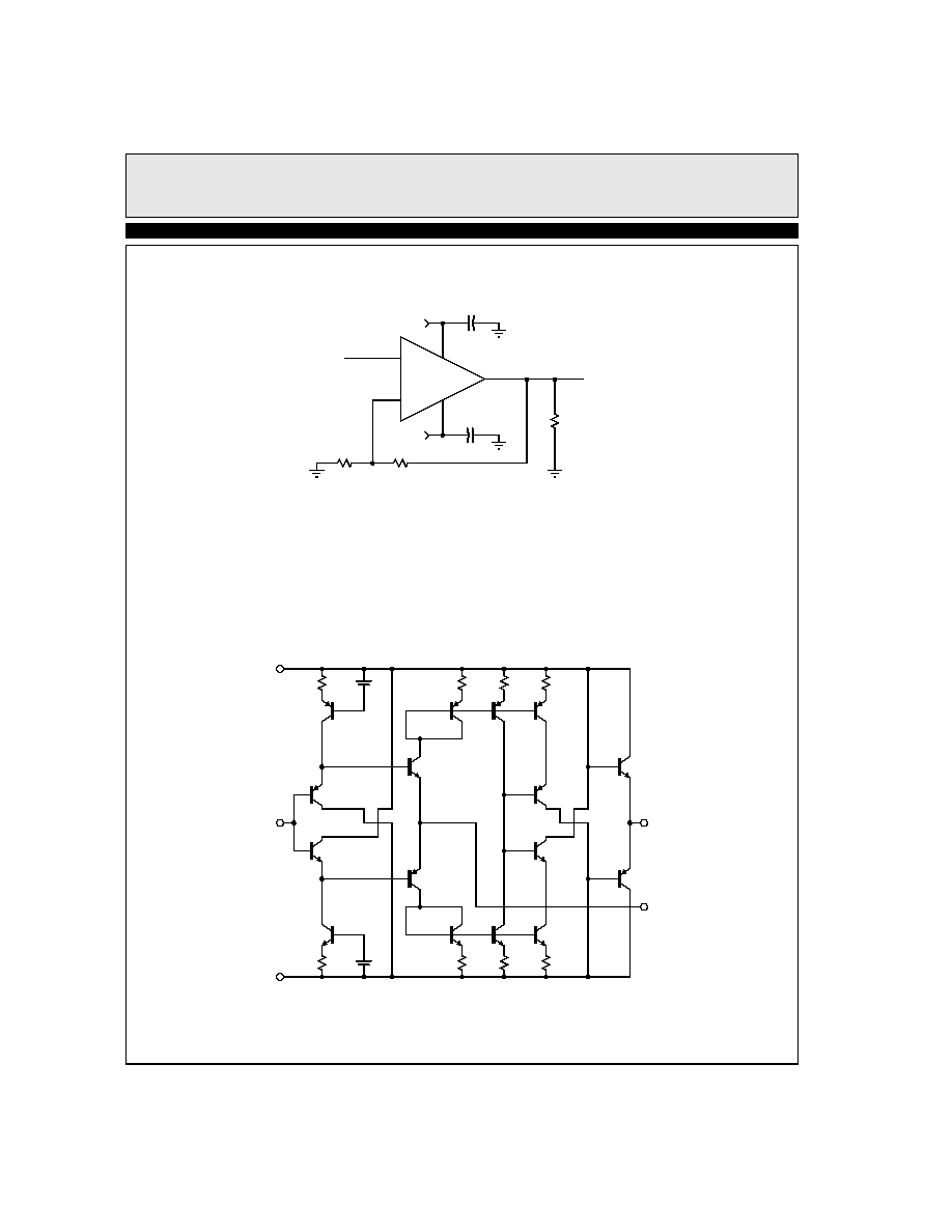
Test Circuit (Per Amplifier)
Simplified Schematic (Per Amplifier)
I
N
+
I
N
-
V
IN
R
G
R
F
750
750
V
S
-
V
S
+
OUT
R
L
150
V
OUT
+5V
-5V
0.1µF
0.1µF
EL2180C or
Ω EL2280C or
º EL2480C
*see note
* Note:
I
N
+
V+
V-
R
7
V
2
Q
14
Q
10
Q
6
Q
2
R
2
V
1
R
3
R
4
R
5
Q
3
Q
4
Q
5
Q
7
Q
11
Q
15
Q
16
Q
17
R
8
R
9
R
10
I
N
-
OUT
Q
9
Q
13
Q
12
Q
8

5
EL2180C/EL2280C/EL2480C-Preliminary
250MHz / 3mA Current Mode Feedback Amplifiers
E
L
2
1
8
0
C
/
E
L
2
2
8
0
C
/
E
L
2
4
8
0
C
-
P
r
e
l
i
m
i
n
a
r
y
Typical Performance Curves
Non-Inverting Frequency
Response (Gain)
(PDIP and SOIC Packages)
Non≠Inverting Frequency
Response (Phase)
(PDIP and SOIC Packages)
Frequency Response
for Various R
F
and R
G
(PDIP and SOIC Packages)
Inverting Frequency
Response (Gain)
(PDIP and SOIC Packages)
Inverting Frequency
Response (Phase)
(PDIP and SOIC Packages)
Frequency Response
for Various R
L
and C
L
(PDIP and SOIC Packages)
Frequency Response for
Various C
IN
-
PSRR and CMRR
vs Frequency
Transimpedance (R
OL
) vs
Frequency