 | –≠–ª–µ–∫—Ç—Ä–æ–Ω–Ω—ã–π –∫–æ–º–ø–æ–Ω–µ–Ω—Ç: EL4089C | –°–∫–∞—á–∞—Ç—å:  PDF PDF  ZIP ZIP |

EL4089C
January
1996
Rev
B
EL4089C
DC Restored Video Amplifier
Note All information contained in this data sheet has been carefully checked and is believed to be accurate as of the date of publication however this data sheet cannot be a ``controlled document'' Current revisions if any to these
specifications are maintained at the factory and are available upon your request We recommend checking the revision level before finalization of your design documentation
1993 Elantec Inc
Features
Complete video level restoration
system
0 02% differential gain and 0 05
differential phase accuracy at
NTSC
60 MHz bandwidth
0 1 dB flatness to 10 MHz
V
S
e
g
5V to
g
15V
TTL CMOS hold signal
Applications
Input amplifier in video
equipment
Restoration amplifier in video
mixers
Ordering Information
Part No
Temp Range
Package
Outline
EL4089CN
0 C to
a
75 C
8-Pin P-DIP
MDP0031
EL4089CS
0 C to
a
75 C
8-Lead SO
MDP0027
General Description
The EL4089C is an 8-pin complete DC-restored monolithic vid-
eo amplifier sub-system It contains a high quality video ampli-
fier and a nulling sample-and-hold amplifier specifically de-
signed to stabilize video performance
When the HOLD logic input is set to a TTL CMOS logic 0 the
sample- and-hold amplifier can be used to null the DC offset of
the video amplifer
When the HOLD input goes to a TTL CMOS logic l the cor-
recting voltage is stored on the video amplifier's input coupling
capacitor The correction voltage can be further corrected as
need be on each video line
The video amplifier is optimized for video performance and low
power Its current feedback design allows the user to maintain
essentially the same bandwidth over a gain range of nearly 10 1
The amplifier drives back-terminated 75
X lines
The EL4089C is fabricated in Elantec's proprietary Comple-
mentary Bipolar process which produces NPN and PNP tran-
sistors with equivalent AC and DC performance The EL4089C
is specified for operation over 0 C to
a
75 C temperature range
Connection Diagram
4089 ≠ 1
DC restoring amplifier with a gain of 2 restoring to ground
EL4089C
DC Restored Video Amplifier
Absolute Maximum Ratings
(T
A
e
25 C)
Voltage between V
a
and V
b
33V
Voltage between V
INa
S H
INa
(V
a
)
a
0 5V
and GND pins
to (V
b
)
b
0 5V
V
OUT
Current
60 mA
Current into V
INb
and HOLD Pins
5 mA
Internal Power Dissipation
See Curves
Operating Ambient
Temperature Range
0 C to
a
75 C
Operating Junction Temperature
Plastic DIP or SOL
150 C
Storage Temperature Range
b
65 C to
a
150 C
Important Note
All parameters having Min Max specifications are guaranteed The Test Level column indicates the specific device testing actually
performed during production and Quality inspection Elantec performs most electrical tests using modern high-speed automatic test
equipment specifically the LTX77 Series system Unless otherwise noted all tests are pulsed tests therefore T
J
e
T
C
e
T
A
Test Level
Test Procedure
I
100% production tested and QA sample tested per QA test plan QCX0002
II
100% production tested at T
A
e
25 C and QA sample tested at T
A
e
25 C
T
MAX
and T
MIN
per QA test plan QCX0002
III
QA sample tested per QA test plan QCX0002
IV
Parameter is guaranteed (but not tested) by Design and Characterization Data
V
Parameter is typical value at T
A
e
25 C for information purposes only
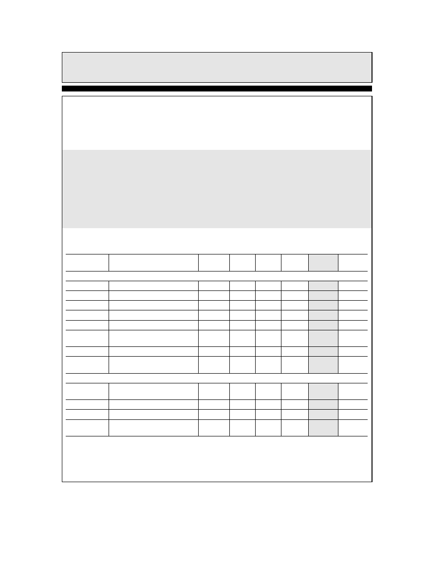
Open Loop DC Electrical Characteristics
Provisional Supplies at
g
15V Load
e
1 k
X T
A
e a
25 C
Parameter
Description
Temp
Min
Typ
Max
Test
Units
Level
Amplifier Section (HOLD
e
5V)
V
OS
Input Offset Voltage
a
25 C
12
25
II
mV
Ib
a
IN
a
Input Bias Current
a
25 C
1
5
II
mA
Ib
b
IN
b
Input Bias Current
a
25 C
18
150
II
mA
R
OL
Transimpedance (Note 1)
a
25 C
180
800
II
k
X
R
INb
IN
b
Resistance
a
25 C
20
V
X
CMRR
Common Mode Rejection Ratio
a
25 C
44
60
II
dB
(Note 2)
V
O
Output Voltage Swing
a
25 C
g
12
g
13
II
V
I
SC
Short Circuit Current
a
25 C
45
100
II
mA
(IN
a
Only Driven to 0 5V)
Restore Section
V
OS
Comp
Composite Input Offset Voltage
a
25 C
3
7
II
mV
(Note 3)
Ib
a
r
Restore In
a
Input Bias Current
a
25 C
3
12
II
mA
I
OUT
Restoring Current Available
a
25 C
180
300
II
mA
CMRR
Common Mode Rejection Ratio
a
25 C
60
70
II
dB
(Note 2)
2
TD
is
35in

EL4089C
DC Restored Video Amplifier
Open Loop DC Electrical Characteristics
Contd
Provisional Supplies at
g
15V Load
e
1 k
X T
A
e a
25 C
Parameter
Description
Temp
Min
Typ
Max
Test
Units
Level
Restore Section
Contd
PSRR
Power Supply Rejection Ratio (Note 4)
a
25 C
60
90
II
dB
V
THRESHOLD
HOLD Logic Threshold
a
25 C
0 8
2 0
II
V
I
IH
Hold
HOLD Input Current
Logic High
a
25 C
1
5
II
mA
I
IL
Hold
HOLD Input Current
Logic Low
a
25 C
5
15
II
mA
Supply Current
Isy Hold
Supply Current (HOLD
e
5V)
a
25 C
4 8
6 0
9 0
II
mA
Isy Sampling
Supply Current (HOLD
e
0V)
a
25 C
5 0
6 5
11 0
II
mA
Closed Loop AC Electrical Characteristics
Provisional Supplies at
g
15V Load
e
150
X and 15 pF R
f
and R
g
e
300
X A
V
e
2 T
A
e
25 C (See Note 7 about Test Fixture)
Parameter
Description
Min
Typ
Max
Test
Units
Level
Amplifier Section
SR
Slew Rate (Note 5)
500
V
V
ms
SR
Slew Rate with
g
5V Supplies
275
V
V
ms
(Note 5)
BW
Bandwidth
b
3 dB
60
V
MHz
g
5V Supplies
b
3 dB
55
V
MHz
BW
Bandwidth
g
0 1 dB
25
V
MHz
g
5V Supplies
g
0 1 dB
23
V
MHz
dG
Differential Gain
V
S
e
g
15V
0 02
V
%
at 3 58 MHz (Note 6)
V
S
e
g
5V
0 03
V
%
dPh
Differential Phase
V
S
e
g
15V
0 05
V
at 3 58 MHz (Note 6)
V
S
e
g
5V
0 06
V
Restore Section
SR
Restore Amplifier Slew Rate
25
V
V
ms
(Test Circuit) 20% ≠ 80%
T
HE
Time to Enable Hold
25
V
ns
T
HD
Time to Disable Hold
40
V
ns
Note 1 For current feedback amplifiers A
VOL
e
R
OL
R
INb
Note 2 V
CM
e
g
10V for V
S
e
g
15V
Note 3 Measured from S H Input to amplifier output while restoring
Note 4 V
OS
is measured at V
S
e
g
4 5V and V
S
e
g
16V both supplies are changed simultaneously
Note 5 SR measured at 20% to 80% of a 4V pk-pk square wave
Note 6 DC offset from
b
0 714V through
a
0 714V ac amplitude is 286 mVp-p equivalent to 40 ire
Note 7 Test fixture was designed to minimize capacitance at the IN
b
input A ``good'' fixture should have less than 2 pF of stray
capacitance to ground at this very sensitive pin See application notes for further details
3
TD
is
32in
TD
is
32in

EL4089C
DC Restored Video Amplifier
Typical Performance Curves
Supply Current vs Temperature
V
S
e
g
15V
4089 ≠ 2
Supply Current
vs Supply Voltage
4089 ≠ 3
Restoring Current
vs Temperature
4089 ≠ 4
Amplifier Input Current
vs Die Temperature
4089 ≠ 5
Amplifier Output Voltage
vs Die Temperature
V
S
e
g
15V
4089 ≠ 6
Amplifier Offset Voltage
vs Die Temperature
4089 ≠ 7
4

EL4089C
DC Restored Video Amplifier
Typical Performance Curves
Contd
CMRR for Amplifier and
Restore Section
vs Die Temperature
4089 ≠ 8
Transimpedance (R
OL
)
vs Die Temperature
4089 ≠ 9
Relative Frequency Response
for Various Gains R
F
e
300X
4089 ≠ 10
Frequency Response vs Supply
A
V
e
2 R
F
e
300
4089 ≠ 11
Frequency Response Flatness vs Supply
A
V
e
2 R
F
e
300
4089 ≠ 12
Frequency Response Flatness for Various
Load and Supply Conditions
A
V
e
2 R
F
e
300
4089 ≠ 13
5