 | –≠–ª–µ–∫—Ç—Ä–æ–Ω–Ω—ã–π –∫–æ–º–ø–æ–Ω–µ–Ω—Ç: EL4393C | –°–∫–∞—á–∞—Ç—å:  PDF PDF  ZIP ZIP |
EL4393C
January
1996
Rev
B
EL4393C
Triple 80 MHz Video Amplifier w Disable
Note All information contained in this data sheet has been carefully checked and is believed to be accurate as of the date of publication however this data sheet cannot be a ``controlled document'' Current revisions if any to these
specifications are maintained at the factory and are available upon your request We recommend checking the revision level before finalization of your design documentation
1993 Elantec Inc
Features
80 MHz
b
3 dB bandwidth for
gains of 1 to 10
900 V ms slew rate
10 MHz bandwidth flat to 0 1 dB
Excellent differential gain and
phase
TTL CMOS compatible
Available in SOL-16
Applications
RGB drivers
RGB multiplexers
RGB gain blocks
Video gain blocks
Coax cable driver
ADC drivers input multiplexer
Ordering Information
Part No
Temp Range
Package
Outline
EL4393CN
b
40 C to
a
85 C 16-Lead P-DIP MDP0031
EL4393CM
b
40 C to
a
85 C 16-Lead SOL
MDP0027
General Description
The EL4393C is three wideband current-feedback amplifiers op-
timized for video performance Each amplifier can drive a load
of 150
X at video levels Each amplifier has a disable capability
which is controlled by a TTL CMOS compatible logic signal
The EL4393C operates on supplies as low as
g
4V up to
g
15V
Being a current-feedback design the bandwidth stays relatively
constant at approximately 80 MHz over the
g
1 to
g
10 gain
range The EL4393C has been optimized for use with 1300
X
feedback resistors at a gain of 2
When the outputs are disabled the supply current consumption
drops by about 4 mA per channel that is disabled This feature
can be used to reduce power dissipation
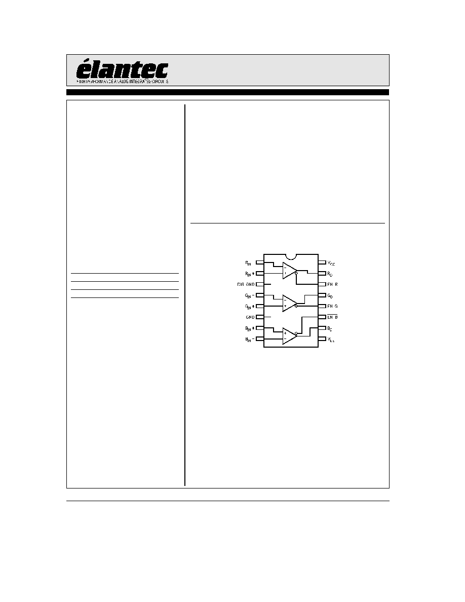
Connection Diagram
4393 ≠ 1

EL4393C
Triple 80 MHz Video Amplifier w Disable
Absolute Maximum Ratings
(T
A
e
25 C)
Voltage between V
S
a
and V
S
b
a
33V
Voltage at V
S
a
a
18V
Voltage at V
S
b
b
18V
Voltage between V
IN
a
and V
IN
b
g
6V
Current into V
IN
a
or V
IN
b
5 mA
Internal Power Dissipation
See Curves
Operating Ambient Temperature Range
b
40 C to
a
85 C
Operating Junction Temperature
150 C
Storage Temperature Range
b
65 C to
a
150 C
Important Note
All parameters having Min Max specifications are guaranteed The Test Level column indicates the specific device testing actually
performed during production and Quality inspection Elantec performs most electrical tests using modern high-speed automatic test
equipment specifically the LTX77 Series system Unless otherwise noted all tests are pulsed tests therefore T
J
e
T
C
e
T
A
Test Level
Test Procedure
I
100% production tested and QA sample tested per QA test plan QCX0002
II
100% production tested at T
A
e
25 C and QA sample tested at T
A
e
25 C
T
MAX
and T
MIN
per QA test plan QCX0002
III
QA sample tested per QA test plan QCX0002
IV
Parameter is guaranteed (but not tested) by Design and Characterization Data
V
Parameter is typical value at T
A
e
25 C for information purposes only
Open Loop DC Electrical Characteristics
Supplies at
g
15V Load
e
1 K
X
Parameter
Description
Temp
Min
Typ
Max
Test
Units
Level
V
OS
Input Offset Voltage
a
25 C
2
g
15
I
mV
TCV
OS
Temperature Coefficient of V
OS
Full
50
V
mV C
I
B
a
I
IN
a
Input Bias Current
a
25 C
0 2
5
I
mA
I
B
b
I
IN
b
Input Bias Current
a
25 C
10
65
I
mA
TCI
B
b
Temperature Coefficient of I
B
b
Full
25
V
nA C
CMRR
Common-Mode Rejection Ratio
a
25 C
50
58
I
dB
(Note 1)
b
ICMR
I
IN
b
Input Common-Mode Current
a
25 C
3
8
I
mA V
(Note 1)
PSRR
Power Supply Rejection Ratio
a
25 C
50
58
I
dB
(Note 2)
b
IPSR
I
IN
b
Current Supply Rejection
a
25 C
2
5
I
mA V
(Note 2)
R
OL
Transimpedance
a
25 C
100
217
I
k
X
R
IN
IN
a
Input Impedance
a
25 C
2
I
M
X
V
IN
IN
a
Input Range
a
25 C
g
13
g
13 5
I
V
V
O
Output Voltage Swing
a
25 C
g
12
g
13
I
V
R
L
e
1 k
X
2
TD
is
34in

EL4393C
Triple 80 MHz Video Amplifier w Disable
Open Loop DC Electrical Characteristics
Supplies at
g
15V Load
e
1K
X
Contd
Parameter
Description
Temp
Min
Typ
Max
Test
Units
Level
I
SC
Short-Circuit Current (Note 3)
a
25 C
40
70
I
mA
I
O DIS
Output Current when Disabled
a
25 C
5
150
I
mA
DIS V
IL
Disable Voltage for Logic Low
a
25 C
0 8
I
V
DIS V
IH
Disable Voltage for Logic High
a
25 C
2 2
I
V
DIS I
IL
Disable Logic Low Input Current
a
25 C
3
25
I
mA
DIS I
IH
Disable Logic High Input Current
a
25 C
0
5
I
mA
I
CC (en)
Positive Supply Current all
a
25 C
15
20
g
29
I
mA
Channels Enabled
I
CC (dis)
Positive Supply Current all
a
25 C
6
11
16
I
mA
Channels Disabled
I
EE (en)
Negative Supply Current all
a
25 C
13
18
g
28
I
mA
Channels Enabled
I
EE (dis)
Negative Supply Current all
a
25 C
4
9
14
I
mA
Channels Disabled
Note 1 V
CM
e
g
10V for V
S
e
g
15V
Note 2 V
OS
is measured at V
S
e
g
4 5V and V
S
e
g
16V both supplies are changed simultaneously
Note 3 Only one output short circuited Pulse test or use heatsink
Closed Loop AC Electrical Characteristics
Supplies at
g
15V Load
e
150
X and 15 pF except
where noted Rf1 and Rf2
e
1500
X A
V
e
2 T
A
e
25 C (See note 8 re test fixture)
Parameter
Description
Min
Typ
Max
Test
Units
Level
SR
Slew Rate (Note 4)
960
V
V
ms
SR
Slew Rate w
g
5V Supplies (Note 5)
470
IV
V
ms
t
s
Settling Time to 1% 5V
p-p
5V Step (Note 6)
32
V
ns
BW
Bandwidth
b
3 dB
80
IV
MHz
g
5V Supplies
b
3 dB
60
IV
MHz
BW
Bandwidth
b
0 1 dB
16
IV
MHz
g
5V Supplies
b
0 1 dB
21
IV
MHz
Peaking
b
3 dB BW Tests
0 6
IV
dB
dG
Differential Gain at 3 58 MHz
0 03
V
%
at
g
5V Supplies (Note 7)
0 30
V
%
d
i
Differential Phase at 3 58 MHz
0 088
V
( )
at
g
5V Supplies (Note 7)
0 096
V
( )
Note 4 R
L
e
300
X
b
5V to
a
5V swing SR measured at 20% to 80%
Note 5
b
2V to
a
2V swing SR measured at 20% to 80%
Note 6 R
L
e
300
X
Note 7 DC offset from
b
0 7V through
a
0 7V AC amplitude is 286 mV
P-P
equivalent to 40 ire
Note 8 Test fixture was designed to minimize capacitance at the I
N
a
input A ``good'' fixture should have less than 2 pF of stray
capacitance to ground at this very sensitive pin See application notes for further details
3
TD
is
27in
TD
is
24in
EL4393C
Triple 80 MHz Video Amplifier w Disable
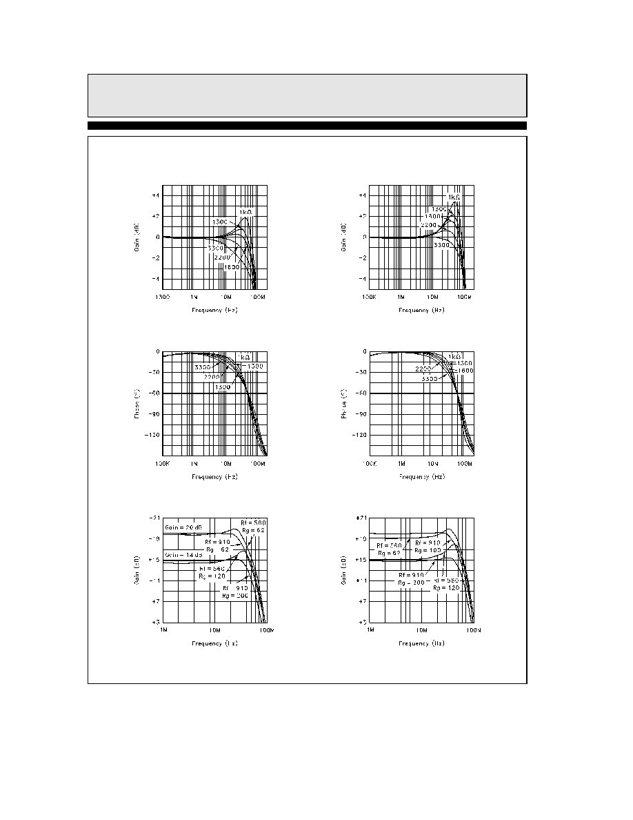
Typical Performance Curves
Gain Flatness vs Rf at
g
5V
Gain Flatness vs Rf at
g
15V
Phase vs Rf at
g
5V
Phase vs Rf at
g
15V
Rg at
g
5V
Gain of 5 10 vs Various Rf
Rg at
g
15V
Gain of 5 10 vs Rf
4393 ≠ 3
4

EL4393C
Triple 80 MHz Video Amplifier w Disable
Typical Performance Curves
Contd
Isolation Test at
g
5V
Disabled
Isolation Test at
g
15V
Disabled
Cin
vs Peaking
Voltage Noise
at 3 58 MHz
Differential Gain
Phase
Channel Isolation
EL4393 MUX Channel
4393 ≠ 11
5