 | –≠–ª–µ–∫—Ç—Ä–æ–Ω–Ω—ã–π –∫–æ–º–ø–æ–Ω–µ–Ω—Ç: EL8202 | –°–∫–∞—á–∞—Ç—å:  PDF PDF  ZIP ZIP |

1
Æ
FN7106
EL8202, EL8203, EL8403
500MHz Rail-to-Rail Amplifiers
The EL8202, EL8203, and EL8403
represent rail-to-rail amplifiers with a
-3dB bandwidth of 500MHz and slew
rate of 600V/µs. Running off a very low supply current of
5.6mA per channel, the EL8202, EL8203, and EL8403 also
feature inputs that go to 0.15V below the V
S
- rail. The
EL8202 and EL8203 are dual channel amplifiers. The
EL8403 is a quad channel amplifier.
The EL8202 includes a fast-acting disable/power-down
circuit. With a 25ns disable and a 200ns enable, the EL8202
is ideal for multiplexing applications.
The EL8202, EL8203, and EL8403 are designed for a
number of general purpose video, communication,
instrumentation, and industrial applications. The EL8202 is
available in a 10-pin MSOP package, the EL8203 in an 8-pin
SO package, and the EL8403 in 14-pin SO and 16-pin
QSOP packages. All are specified for operation over the
-40∞C to +85∞C temperature range.
Features
∑ 500MHz -3dB bandwidth
∑ 600V/µs slew rate
∑ Low supply current = 5.6mA per channel
∑ Supplies from 3V to 5.5V
∑ Rail-to-rail output
∑ Input to 0.15V below V
S
-
∑ Fast 25ns disable (EL8202 only)
∑ Low cost
Applications
∑ Video amplifiers
∑ Portable/hand-held products
∑ Communications devices
Ordering Information
PART
NUMBER
PACKAGE
TAPE & REEL PKG. DWG. #
EL8202IY
10-Pin MSOP
-
MDP0043
EL8202IY-T7
10-Pin MSOP
7"
MDP0043
EL8202IY-T13
10-Pin MSOP
13"
MDP0043
EL8203IS
8-Pin SO
-
MDP0027
EL8203IS-T7
8-Pin SO
7"
MDP0027
EL8203IS-T13
8-Pin SO
13"
MDP0027
EL8403IS
14-Pin SO
-
MDP0027
EL8403IS-T7
14-Pin SO
7"
MDP0027
EL8403IS-T13
14-Pin SO
13"
MDP0027
EL8403IU
16-Pin QSOP
-
MDP0040
EL8403IU-T7
16-Pin QSOP
7"
MDP0040
EL8403IU-T13
16-Pin QSOP
13"
MDP0040
Data Sheet
November 20, 2003
CAUTION: These devices are sensitive to electrostatic discharge; follow proper IC Handling Procedures.
1-888-INTERSIL or 321-724-7143
|
Intersil (and design) is a registered trademark of Intersil Americas Inc.
Copyright © Intersil Americas Inc. 2003. All Rights Reserved. Elantec is a registered trademark of Elantec Semiconductor, Inc.
All other trademarks mentioned are the property of their respective owners.

2
Pinouts
EL8203
(8-PIN SO)
TOP VIEW
EL8202
(10-PIN MSOP)
TOP VIEW
EL8403
(14-PIN SO)
TOP VIEW
EL8403
(16-PIN QSOP)
TOP VIEW
1
2
3
4
8
7
6
5
-
+
-
+
OUTA
INA-
INA+
VS-
VS+
OUTB
INB-
INB+
-
+
-
+
INA+
CEA
VS-
CEB
INA-
OUTA
VS+
OUTB
INB+
INB-
1
2
3
4
10
9
8
7
5
6
1
2
3
4
14
13
12
11
5
6
7
10
9
8
OUTA
INA-
INA+
VS+
INB+
INB-
OUTB
OUTD
IND-
IND+
VS-
INC+
INC-
OUTC
- +
-
+
- +
-
+
A
D
B
C
1
2
3
4
16
15
14
13
5
6
7
12
11
10
8
9
OUTA
INA-
INA+
VS+
INB+
INB-
OUTB
OUTD
IND-
IND+
VS-
INC+
INC-
OUTC
NC
NC
- +
-
+
- +
-
+
EL8202, EL8203, EL8403
3
IMPORTANT NOTE: All parameters having Min/Max specifications are guaranteed. Typ values are for information purposes only. Unless otherwise noted, all tests are
at the specified temperature and are pulsed tests, therefore: T
J
= T
C
= T
A
Absolute Maximum Ratings
(T
A
= 25∞C)
Supply Voltage from V
S
+ to V
S
- . . . . . . . . . . . . . . . . . . . . . . . . 5.5V
Input Voltage . . . . . . . . . . . . . . . . . . . . . . . . V
S
+ +0.3V to V
S
- -0.3V
Differential Input Voltage . . . . . . . . . . . . . . . . . . . . . . . . . . . . . . . .2V
Continuous Output Current . . . . . . . . . . . . . . . . . . . . . . . . . . . 40mA
Power Dissipation . . . . . . . . . . . . . . . . . . . . . . . . . . . . . See Curves
Storage Temperature . . . . . . . . . . . . . . . . . . . . . . . .-65∞C to +150∞C
Ambient Operating Temperature . . . . . . . . . . . . . . . .-40∞C to +85∞C
Operating Junction Temperature . . . . . . . . . . . . . . . . . . . . . . +125∞C
CAUTION: Stresses above those listed in "Absolute Maximum Ratings" may cause permanent damage to the device. This is a stress only rating and operation of the
device at these or any other conditions above those indicated in the operational sections of this specification is not implied.
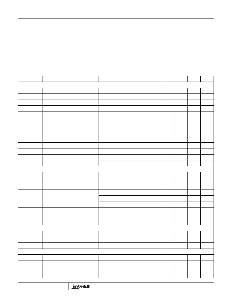
Electrical Specifications
V
S
+
= 5V, V
S
-
= GND, T
A
= 25∞C, V
CM
= 2.5V, R
L
to 2.5V, A
V
= 1, Unless Otherwise Specified
PARAMETER
DESCRIPTION
CONDITIONS
MIN
TYP
MAX
UNIT
INPUT CHARACTERISTICS
V
OS
Offset Voltage
-8
-0.8
+8
mV
TCV
OS
Offset Voltage Temperature Coefficient
Measured from T
MIN
to T
MAX
3
µV/∞C
IB
Input Bias Current
V
IN
= 0V
-9
-6
µA
I
OS
Input Offset Current
V
IN
= 0V
0.1
0.6
µA
TCI
OS
Input Bias Current Temperature
Coefficient
Measured from T
MIN
to T
MAX
2
nA/∞C
CMRR
Common Mode Rejection Ratio
V
CM
= -0.15V to +3.5V (EL8202,EL8203)
70
95
dB
V
CM
= -0.15V to +3.5V (EL8403)
60
85
dB
CMIR
Common Mode Input Range
V
S
- -
0.15
V
S
+ -
1.5
V
R
IN
Input Resistance
Common Mode
3.5
M
C
IN
Input Capacitance
0.5
pF
AVOL
Open Loop Gain
V
OUT
= +1.5V to +3.5V, R
L
= 1k
to GND
75
90
dB
V
OUT
= +1.5V to +3.5V, R
L
= 150
to GND
80
dB
OUTPUT CHARACTERISTICS
R
OUT
Output Resistance
A
V
= +1
30
m
V
OP
Positive Output Voltage Swing
R
L
= 1k
4.85
4.9
V
R
L
= 150
4.6
4.7
V
V
ON
Negative Output Voltage Swing
R
L
= 150
100
150
mV
R
L
= 1k
(EL8202,EL8203)
25
50
mV
R
L
= 1k
(EL8403)
50
100
mV
I
OUT
Linear Output Current
65
mA
I
SC
(source)
Short Circuit Current
R
L
= 10
60
80
mA
I
SC
(sink)
Short Circuit Current
R
L
= 10
120
150
mA
POWER SUPPLY
PSRR
Power Supply Rejection Ratio
V
S
+ = 4.5V to 5.5V
70
95
dB
I
S-ON
Supply Current - Enabled (per amplifier)
5.6
6.2
mA
I
S-OFF
Supply Current - Disabled (per amplifier)
40
90
µA
ENABLE (EL8202 ONLY)
t
EN
Enable Time
200
ns
t
DS
Disable Time
25
ns
V
IH-ENB
ENABLE Pin Voltage for Power-up
0.8
V
V
IL-ENB
ENABLE Pin Voltage for Shut-down
2
V
EL8202, EL8203, EL8403

4
I
IH-ENB
ENABLE Pin Input Current High
8.6
µA
I
IL-ENB
ENABLE Pin Input for Current Low
0.01
µA
AC PERFORMANCE
BW
-3dB Bandwidth
A
V
= +1, R
F
= 0
, C
L
= 2.5pF
500
MHz
A
V
= -1, R
F
= 1k
, C
L
= 2.5pF
140
MHz
A
V
= +2, R
F
= 1k
, C
L
= 2.5pF
165
MHz
A
V
= +10, R
F
= 1k
, C
L
= 2.5pF
18
MHz
BW
±0.1dB Bandwidth
A
V
= +1, R
F
= 0
, C
L
= 2.5pF
35
MHz
Peak
Peaking
A
V
= +1, R
L
= 1k
, C
L
= 2.5pF
2
dB
GBWP
Gain Bandwidth Product
200
MHz
PM
Phase Margin
R
L
= 1k
, C
L
= 2.5pF
55
∞
SR
Slew Rate
A
V
= 2, R
L
= 100
, V
OUT
= 0.5V to 4.5V
500
600
V/µs
t
R
Rise Time
2.5V
STEP
, 20% - 80%
4
ns
t
F
Fall Time
2.5V
STEP
, 20% - 80%
2
ns
OS
Overshoot
200mV step
10
%
t
PD
Propagation Delay
200mV step
1
ns
t
S
0.1% Settling Time
200mV step
15
ns
dG
Differential Gain
A
V
= +2, R
F
= 1k
, R
L
= 150
0.01
%
dP
Differential Phase
A
V
= +2, R
F
= 1k
, R
L
= 150
0.01
∞
e
N
Input Noise Voltage
f = 10kHz
12
nV/
Hz
i
N
+
Positive Input Noise Current
f = 10kHz
1.7
pA/
Hz
i
N
-
Negative Input Noise Current
f = 10kHz
1.3
pA/
Hz
e
S
Channel Separation
f = 100kHz
95
dB
Electrical Specifications
V
S
+
= 5V, V
S
-
= GND, T
A
= 25∞C, V
CM
= 2.5V, R
L
to 2.5V, A
V
= 1, Unless Otherwise Specified (Continued)
PARAMETER
DESCRIPTION
CONDITIONS
MIN
TYP
MAX
UNIT
Pin Descriptions
EL8202
EL8203
EL8403
(SO-14)
EL8403
(QSOP-16)
NAME
FUNCTION
1, 5
3, 5
3, 5, 10, 12
3,5,12,14
IN+
Non-inverting input for each channel
2, 4
CE
Enable and disable input for each channel
3
4
11
13
VS-
Negative power supply
6, 10
2, 6
2, 6, 9, 13
2,6,11,15
IN-
Inverting input for each channel
7, 9
1, 7
1, 7, 8, 14
1,7,10,16
OUT
Amplifier output for each channel
8
8
4
4
VS+
Positive power supply
EL8202, EL8203, EL8403

5
Typical Performance Curves
FIGURE 1. FREQUENCY RESPONSE FOR VARIOUS OUTPUT
VOLTAGE LEVELS
FIGURE 2. SMALL SIGNAL FREQUENCY RESPONSE
vs R
F
AND R
G
FIGURE 3. SMALL SIGNAL FREQUENCY RESPONSE FOR
VARIOUS NON-INVERTING GAINS
FIGURE 4. SMALL SIGNAL FREQUENCY RESPONSE FOR
VARIOUS INVERTING GAINS
FIGURE 5. SMALL SIGNAL FREQUENCY RESPONSE FOR
VARIOUS NON-INVERTING GAINS
FIGURE 6. SMALL SIGNAL FREQUENCY RESPONSE vs
VARIOUS R
LOAD
5
3
1
-1
-3
-5
1M
10M
100M
1G
FREQUENCY (Hz)
GAI
N
(
d
B)
V
S
=5V
A
V
=1
R
L
=1k
C
L
=2.5pF
4
2
0
-2
-4
V
OP-P
=200mV
V
OP-P
=1V
V
OP-P
=2V
5
3
1
-1
-3
-5
100K
1M
10M
100M
1G
FREQUENCY (Hz)
NORMALIZED GAIN
(
d
B)
V
S
=5V
A
V
=2
R
L
=1k
C
L
=2.5pF
R
F
=R
G
=2k
R
F
=R
G
=500
R
F
=R
G
=1k
5
3
1
-1
-3
-5
1M
10M
100M
1G
FREQUENCY (Hz)
NORMALIZED GAIN
(
d
B)
A
V
=10
A
V
=1
V
S
=5V
C
L
=2.5pF
R
L
=1k
A
V
=5
A
V
=2
4
2
0
-2
-4
4
2
0
-2
-4
-6
100K
1M
10M
100M
1G
FREQUENCY (Hz)
NORMALIZED GAIN
(dB)
A
V
=-10
V
S
=5V
C
L
=2.5pF
R
L
=1k
R
F
=1k
A
V
=-1
A
V
=-5
5
3
1
-1
-3
-5
1M
10M
100M
1G
FREQUENCY (Hz)
GAI
N
(
d
B)
R
L
=1k
V
S
=5V
A
V
=1
C
L
=2.5pF
4
2
0
-2
-4
R
L
=100
R
L
=500
11
9
7
5
3
1
100K
1M
10M
100M
1G
FREQUENCY (Hz)
GAI
N
(
d
B)
V
S
=5V
A
V
=2
C
L
=2.5pF
R
F
=R
G
=1k
R
L
=500
R
L
=1k
,
150
EL8202, EL8203, EL8403