Document Outline
- COVER
- Description
- Features
- Ordering Information
- Pin Configuration
- Block Diagram
- Electrical Specifications
- Absolute Maximum Ratings
- Recommended Operating Conditions
- Capacitance
- DC Characteristics
- AC Characteristics
- Test Conditions
- Synchronous Characteristics
- Asynchronous Characteristics
- Serial PD
- Timing Chart
- Package Drawing
The information in this document is subject to change without notice. Before using this document, please
confirm that this is the latest version.
Not all devices/types available in every country. Please check with local Elpida Memory, Inc. for
availability and additional information.
MOS INTEGRATED CIRCUIT
MC-4532CD647XFA
32M-WORD BY 64-BIT SYNCHRONOUS DYNAMIC RAM MODULE
UNBUFFERED TYPE
DATA SHEET
Document No. E0230N20 (Ver 2.0)
Date Published June 2002 (K) Japan
URL: http://www.elpida.com
Elpida Memory, Inc. 2001-2002
Elpida Memory, Inc. is a joint venture DRAM company of NEC Corporation and Hitachi, Ltd.
Description
The MC-4532CD647XFA is 33,554,432 words by 64 bits synchronous dynamic RAM module on which 16 pieces of
128M SDRAM:
�
PD45128841 are assembled.
This module provides high density and large quantities of memory in a small space without utilizing the surface-
mounting technology on the printed circuit board.
Decoupling capacitors are mounted on power supply line for noise reduction.
Features
�
33,554,432 words by 64 bits organization
�
Clock frequency and access time from CLK.
Part number
/CAS latency
Clock frequency
(MAX.)
Access time from CLK
(MAX.)
MC-4532CD647XFA-A75
CL = 3
133 MHz
5.4
ns
CL = 2
100 MHz
6.0 ns
�
Fully Synchronous Dynamic RAM, with all signals referenced to a positive clock edge
�
Pulsed interface
�
Possible to assert random column address in every cycle
�
Quad internal banks controlled by BA0 and BA1 (Bank Select)
�
Programmable burst-length (1, 2, 4, 8 and full page)
�
Programmable wrap sequence (Sequential
/
Interleave)
�
Programmable /CAS latency (2, 3)
�
Automatic precharge and controlled precharge
�
CBR (Auto) refresh and self refresh
�
All DQs have 10
�
10
% of series resistor
�
Single 3.3
V
�
0.3
V power supply
�
LVTTL compatible
�
4,096 refresh cycles/64
ms
�
Burst termination by Burst Stop command and Precharge command
�
168-pin dual in-line memory module (Pin pitch = 1.27
mm)
�
Unbuffered type
�
Serial PD

2
MC-4532CD647XFA
Data Sheet E0230N20 (Ver. 2.0)
Ordering Information
Part number
Clock frequency
(MAX.)
Package Mounted
devices
MC-4532CD647XFA-A75
133 MHz
168-pin Dual In-line Memory
16 pieces of
�
PD45128841G5 (Rev. X)
Module (Socket Type)
(10.16 mm (400) TSOP (II))
Edge connector: Gold plated
34.93 mm height

3
MC-4532CD647XFA
Data Sheet E0230N20 (Ver. 2.0)
Pin Configuration
168-pin Dual In-line Memory
Module Socket Type (Edge connector: Gold plated)
85
86
87
88
89
90
91
92
93
94
95
96
97
98
99
100
101
102
103
104
105
106
107
108
109
110
111
112
113
114
115
116
117
118
119
120
121
122
123
124
125
126
127
128
129
130
131
132
133
134
135
136
137
138
139
140
141
142
143
144
145
146
147
148
149
150
151
152
153
154
155
156
157
158
159
160
161
162
163
164
165
166
167
168
V
SS
DQ32
DQ33
DQ34
DQ35
Vcc
DQ36
DQ37
DQ38
DQ39
DQ40
V
SS
DQ41
DQ42
DQ43
DQ44
DQ45
Vcc
NC
V
SS
NC
NC
Vcc
/CAS
DQMB4
DQMB5
/CS1
/RAS
V
SS
A1
A3
A5
A7
A9
BA0
(A13)
A11
Vcc
CLK1
NC
V
SS
CKE0
/CS3
DQMB6
DQMB7
NC
Vcc
NC
NC
NC
NC
V
SS
DQ48
DQ49
DQ50
DQ51
Vcc
DQ52
NC
NC
NC
V
SS
DQ53
DQ54
DQ55
V
SS
DQ56
DQ57
DQ58
DQ59
Vcc
DQ60
DQ61
DQ62
DQ63
V
SS
CLK3
NC
SA0
SA1
SA2
Vcc
1
2
3
4
5
6
7
8
9
10
11
12
13
14
15
16
17
18
19
20
21
22
23
24
25
26
27
28
29
30
31
32
33
34
35
36
37
38
39
40
41
42
43
44
45
46
47
48
49
50
51
52
53
54
55
56
57
58
59
60
61
62
63
64
65
66
67
68
69
70
71
72
73
74
75
76
77
78
79
80
81
82
83
84
V
SS
DQ0
DQ1
DQ2
DQ3
Vcc
DQ4
DQ5
DQ6
DQ7
DQ8
V
SS
DQ9
DQ10
DQ11
DQ12
DQ13
Vcc
DQ14
DQ15
NC
NC
V
SS
NC
NC
Vcc
/WE
DQMB0
DQMB1
/CS0
NC
V
SS
A0
A2
A4
A6
A8
A10
BA1 (A12)
Vcc
Vcc
CLK0
V
SS
NC
/CS2
DQMB2
DQMB3
NC
Vcc
NC
NC
NC
NC
V
SS
DQ16
DQ17
DQ18
DQ19
Vcc
DQ20
NC
NC
CKE1
V
SS
DQ21
DQ22
DQ23
V
SS
DQ24
DQ25
DQ26
DQ27
Vcc
DQ28
DQ29
DQ30
DQ31
V
SS
CLK2
NC
NC
SDA
SCL
Vcc
DQ46
DQ47
NC
A0 - A11
: Address Inputs
[Row: A0 - A11, Column: A0 - A9]
BA0 (A13), BA1 (A12)
: SDRAM Bank Select
DQ0 - DQ63
: Data Inputs/Outputs
CLK0 - CLK3
: Clock Input
CKE0, CKE1
: Clock Enable Input
/CS0 - /CS3
: Chip Select Input
/RAS
: Row Address Strobe
/CAS
: Column Address Strobe
/WE :
Write
Enable
DQMB0 - DQMB7 : DQ Mask Enable
SA0 - SA2
: Address Input for EEPROM
SDA
: Serial Data I/O for PD
SCL
: Clock Input for PD
V
CC
: Power Supply
V
SS
: Ground
NC :
No
Connection
/xxx indicates active low signal.
4
MC-4532CD647XFA
Data Sheet E0230N20 (Ver. 2.0)
Block Diagram
DQMB0
/CS0
/WE
DQM
D0
/CS
/WE
D1
DQM
/CS
/WE
D4
/WE
D5
DQM
/CS
/WE
D6
DQM
/CS
/WE
D7
DQM
/CS
/WE
D3
DQM
/CS
/WE
DQM
D2
/CS
/WE
A0 - A11
A0 - A11: D0 - D15
V
CC
D0 - D15
D0 - D15
SERIAL PD
SCL
SDA
A0
A1
A2
SA0 SA1 SA2
DQMB1
DQMB5
DQMB7
DQMB6
DQMB3
D8
/CS
/WE
D9
/CS
/WE
DQ 0
DQ 1
DQ 2
DQ 3
DQ 4
DQ 5
DQ 6
DQ 7
D12
/CS
/WE
DQ 3
DQ 0
DQ 1
DQ 2
DQ 4
DQ 5
DQ 6
DQ 7
D13
/CS
/WE
DQ 2
DQ 0
DQ 1
DQ 3
DQ 4
DQ 5
DQ 6
DQ 7
D10
/WE
D11
DQM
/CS
/WE
DQ 3
DQ 0
DQ 1
DQ 2
DQ 4
DQ 5
DQ 6
DQ 7
D14
DQM
/CS
/WE
DQ 0
DQ 1
DQ 2
DQ 3
DQ 4
DQ 5
DQ 6
DQ 7
D15
/CS
/WE
DQ 0
DQ 1
DQ 2
DQ 3
DQ 4
DQ 5
DQ 6
DQ 7
DQMB2
/CS2
/CS3
/CS1
/CS
DQM
DQM
DQMB4
DQM
/CS
DQM
DQM
DQM
DQM
BA0, BA1
A13, A12: D0 - D15
/RAS
/RAS: D0 - D15
/CAS
/CAS: D0 - D15
CKE0
CKE: D0 - D7
10 k
V
SS
CKE1
CKE: D8-D15
C
DQ 1
DQ 2
DQ 3
DQ 4
DQ 5
DQ 6
DQ 7
DQ 0
DQ 9
DQ 10
DQ 11
DQ 12
DQ 13
DQ 14
DQ 15
DQ 8
DQ 17
DQ 18
DQ 19
DQ 20
DQ 21
DQ 22
DQ 23
DQ 16
DQ 25
DQ 26
DQ 27
DQ 28
DQ 29
DQ 30
DQ 31
DQ 24
DQ 33
DQ 34
DQ 35
DQ 36
DQ 37
DQ 38
DQ 39
DQ 32
DQ 41
DQ 42
DQ 43
DQ 44
DQ 45
DQ 46
DQ 47
DQ 40
DQ 49
DQ 50
DQ 51
DQ 52
DQ 53
DQ 54
DQ 55
DQ 48
DQ 57
DQ 58
DQ 59
DQ 60
DQ 61
DQ 62
DQ 63
DQ 56
DQ 6
DQ 5
DQ 4
DQ 3
DQ 2
DQ 1
DQ 0
DQ 7
DQ 1
DQ 2
DQ 3
DQ 4
DQ 5
DQ 6
DQ 7
DQ 0
DQ 6
DQ 5
DQ 4
DQ 3
DQ 2
DQ 1
DQ 0
DQ 7
DQ 1
DQ 2
DQ 3
DQ 4
DQ 5
DQ 6
DQ 7
DQ 0
DQ 6
DQ 5
DQ 4
DQ 3
DQ 2
DQ 1
DQ 0
DQ 7
DQ 7
DQ 6
DQ 5
DQ 3
DQ 2
DQ 1
DQ 0
DQ 4
DQ 7
DQ 6
DQ 5
DQ 3
DQ 2
DQ 1
DQ 0
DQ 4
DQ 6
DQ 5
DQ 4
DQ 3
DQ 2
DQ 1
DQ 0
DQ 7
DQ 7
DQ 6
DQ 4
DQ 3
DQ 2
DQ 1
DQ 0
DQ 5
DQ 6
DQ 5
DQ 4
DQ 3
DQ 2
DQ 1
DQ 0
DQ 7
CLK0
3.3 pF
CLK2
3.3 pF
CLK1
3.3 pF
CLK3
3.3 pF
C
LK: D0, D1, D4, D5
C
LK: D8, D9, D12, D13
C
LK: D2, D3, D6, D7
C
LK: D10, D11, D14, D15
Remarks 1. The value of all resistors is 10
except CKE1.
2. D0 - D15:
�
PD45128841 (4M words � 8 bits � 4 banks)
5
MC-4532CD647XFA
Data Sheet E0230N20 (Ver. 2.0)
Electrical Specifications
�
All voltages are referenced to V
SS
(GND).
�
After power up, wait more than 100
�
s and then, execute power on sequence and CBR (Auto) refresh before proper
device operation is achieved.
Absolute Maximum Ratings
Parameter Symbol
Condition
Rating
Unit
Voltage on power supply pin relative to GND
V
CC
�0.5
to
+4.6
V
Voltage on input pin relative to GND
V
T
�0.5
to
+4.6
V
Short circuit output current
I
O
50
mA
Power dissipation
P
D
16
W
Operating ambient temperature
T
A
0
to
70
�
C
Storage temperature
T
stg
�55
to
+125
�
C
Caution Exposing the device to stress above those listed in Absolute Maximum Ratings could cause
permanent damage. The device is not meant to be operated under conditions outside the limits
described in the operational section of this specification. Exposure to Absolute Maximum Rating
conditions for extended periods may affect device reliability.
Recommended Operating Conditions
Parameter Symbol
Condition
MIN.
TYP.
MAX.
Unit
Supply voltage
V
CC
3.0
3.3
3.6
V
High level input voltage
V
IH
2.0
V
CC
+
0.3
V
Low level input voltage
V
IL
-
0.3 +0.8 V
Operating ambient temperature
T
A
0
70
�
C
Capacitance (T
A
= 25
�
�
�
�
C, f = 1 MHz)
Parameter Symbol
Test
condition
MIN.
TYP.
MAX.
Unit
Input capacitance
C
I1
A0 - A11, BA0 (A13), BA1 (A12),
/RAS, /CAS, /WE
36 76
pF
C
I2
CLK0
-
CLK3
20
40
C
I3
CKE0,
CKE1
28
52
C
I4
/CS0 - /CS3
15
29
C
I5
DQMB0
-
DQMB7
5
17
Data input/output capacitance
C
I/O
DQ0 - DQ63
7
19
pF
6
MC-4532CD647XFA
Data Sheet E0230N20 (Ver. 2.0)
DC Characteristics (Recommended Operating Conditions Unless Otherwise Noted)
-A75
Parameter Symbol
Test
condition
MIN.
MAX.
Unit
Notes
Operating current
I
CC1
Burst length
=
1
/CAS latency = 2
1,040 mA
1
t
RC
t
RC(MIN.)
, I
O
= 0
mA
/CAS latency = 3
1,080
Precharge standby current in
I
CC2
P CKE
V
IL(MAX.)
, t
CK
=
15
ns
16 mA
power down mode
I
CC2
PS CKE
V
IL(MAX.)
, t
CK
=
16
Precharge standby current in
non power down mode
I
CC2
N CKE
V
IH(MIN.)
, t
CK
=
15
ns, /CS
V
IH(MIN.)
,
Input signals are changed one time during
30
ns.
320 mA
I
CC2
NS CKE
V
IH(MIN.)
, t
CK
=
Input
signals are stable.
128
Active standby current in
I
CC3
P CKE
V
IL(MAX.)
, t
CK
=
15
ns
80 mA
power down mode
I
CC3
PS CKE
V
IL(MAX.)
, t
CK
=
64
Active standby current in non
power down mode
I
CC3
N CKE
V
IH(MIN.)
, t
CK
=
15
ns, /CS
V
IH(MIN.)
,
Input signals are changed one time during
30
ns.
480 mA
I
CC3
NS CKE
V
IH(MIN.)
, t
CK
=
, Input signals are stable.
320
Operating current
I
CC4
t
CK
t
CK(MIN.)
/CAS latency = 2
1,200 mA
2
(Burst mode)
I
O
= 0
mA
/CAS latency = 3
1,480
CBR (Auto) refresh current
I
CC5
t
RC
t
RC(MIN.)
/CAS latency = 2
2,080 mA
3
/CAS latency = 3
2,160
Self refresh current
I
CC6
CKE
0.2
V
32 mA
Input leakage current
I
I(L)
V
I
=
0 to 3.6
V,
All other pins not under
test =
0 V
�
16 +
16
�
A
CKE1
� 500
+500
Output leakage current
I
O(L)
D
OUT
is disabled, V
O
=
0 to 3.6
V
�
3 +
3
�
A
High level output voltage
V
OH
I
O
=
�
4.0
mA
2.4 V
Low level output voltage
V
OL
I
O
=
+
4.0
mA
0.4
V
Notes 1. I
CC1
depends on output loading and cycle rates. Specified values are obtained with the output open. In
addition to this, I
CC1
is measured on condition that addresses are changed only one time during t
CK (MIN.)
.
2. I
CC4
depends on output loading and cycle rates. Specified values are obtained with the output open. In
addition to this, I
CC4
is measured on condition that addresses are changed only one time during t
CK (MIN.)
.
3. I
CC5
is measured on condition that addresses are changed only one time during t
CK (MIN.)
.
7
MC-4532CD647XFA
Data Sheet E0230N20 (Ver. 2.0)
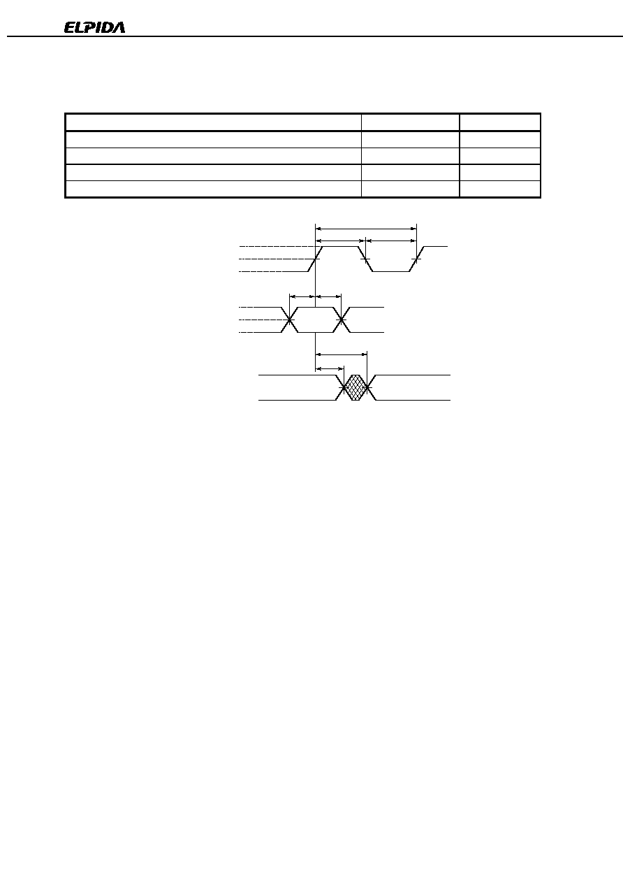
AC Characteristics (Recommended Operating Conditions Unless Otherwise Noted)
Test Conditions
Parameter Value
Unit
AC high level input voltage / low level input voltage
2.4 / 0.4
V
Input timing measurement reference level
1.4
V
Transition time (Input rise and fall time)
1
ns
Output timing measurement reference level
1.4
V
t
CK
t
CH
t
CL
2.4 V
1.4 V
0.4 V
CLK
2.4 V
1.4 V
0.4 V
Input
t
SETUP
t
HOLD
Output
t
AC
t
OH

8
MC-4532CD647XFA
Data Sheet E0230N20 (Ver. 2.0)
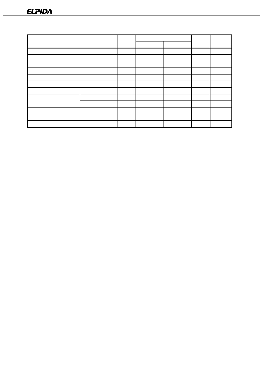
Synchronous Characteristics
Parameter Symbol
-A75
Unit
Note
MIN.
MAX.
Clock cycle time
/CAS latency = 3
t
CK3
7.5 (133
MHz)
ns
/CAS latency = 2
t
CK2
10 (100
MHz)
ns
Access time from CLK
/CAS latency = 3
t
AC3
5.4 ns
1
/CAS latency = 2
t
AC2
6.0 ns
1
CLK high level width
t
CH
2.5
ns
CLK low level width
t
CL
2.5
ns
Data-out hold time
t
OH
3.0
ns 1
Data-out low-impedance time
t
LZ
0
ns
Data-out high-impedance time
/CAS latency = 3
t
HZ3
3.0
5.4 ns
/CAS latency = 2
t
HZ2
3.0
6.0 ns
Data-in setup time
t
DS
1.5
ns
Data-in hold time
t
DH
0.8
ns
Address setup time
t
AS
1.5
ns
Address hold time
t
AH
0.8
ns
CKE setup time
t
CKS
1.5
ns
CKE hold time
t
CKH
0.8
ns
CKE setup time (Power down exit)
t
CKSP
1.5
ns
Command (/CS0 - /CS3, /RAS, /CAS, /WE,
t
CMS
1.5
ns
DQMB0 - DQMB7) setup time
Command (/CS0 - /CS3, /RAS, /CAS, /WE,
t
CMH
0.8
ns
DQMB0 - DQMB7) hold time
Note 1. Output load
Output
Z = 50
50 pF
Remark These specifications are applied to the monolithic device.
9
MC-4532CD647XFA
Data Sheet E0230N20 (Ver. 2.0)
Asynchronous Characteristics
Parameter Symbol
-A75
Unit
Note
MIN.
MAX.
ACT to REF/ACT command period (operation)
t
RC
67.5
ns
REF to REF/ACT command period (refresh)
t
RC1
67.5
ns
ACT to PRE command period
t
RAS
45 120,000
ns
PRE to ACT command period
t
RP
20
ns
Delay time ACT to READ/WRITE command
t
RCD
20
ns
ACT(one) to ACT(another) command period
t
RRD
15
ns
Data-in to PRE command period
t
DPL
8
ns
Data-in to ACT(REF) command /CAS latency = 3
t
DAL3
1CLK+22.5
ns
1
period (Auto precharge)
/CAS latency = 2
t
DAL2
1CLK+20
ns
1
Mode register set cycle time
t
RSC
2
CLK
Transition time
t
T
0.5 30 ns
Refresh time (4,096 refresh cycles)
t
REF
64 ms
Note This device can satisfy the t
DAL3
spec of 1CLK+20 ns for up to and including 125 MHz operation.
10
MC-4532CD647XFA
Data Sheet E0230N20 (Ver. 2.0)
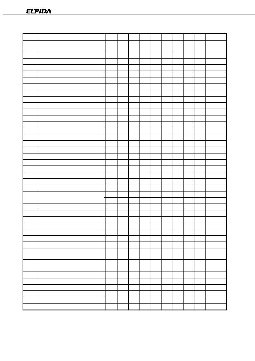
Serial PD
(1/2)
Byte No.
Function Described
Hex
Bit 7 Bit 6 Bit 5 Bit 4 Bit 3 Bit 2 Bit 1 Bit 0
Notes
0
Defines the number of bytes written into
serial PD memory
80H 1 0 0 0 0 0 0 0
128
bytes
1
Total number of bytes of serial PD memory
08H 0 0 0 0 1 0 0 0
256
bytes
2 Fundamental
memory
type
04H 0 0 0 0 0 1 0 0
SDRAM
3 Number
of
rows
0CH 0 0 0 0 1 1 0 0
12
rows
4 Number
of
columns
0AH 0 0 0 0 1 0 1 0
10
columns
5 Number
of
banks
02H 0 0 0 0 0 0 1 0
2
banks
6 Data
width
40H 0 1 0 0 0 0 0 0
64
bits
7 Data
width
(continued)
00H 0 0 0 0 0 0 0 0
0
8 Voltage
interface
01H 0 0 0 0 0 0 0 1
LVTTL
9 CL
=
3
Cycle
time
75H 0 1 1 1 0 1 0 1
7.5
ns
10
CL = 3 Access time
54H
0
1
0
1
0
1
0
0
5.4 ns
11
DIMM
configuration
type
00H 0 0 0 0 0 0 0 0
None
12
Refresh
rate/type
80H 1 0 0 0 0 0 0 0
Normal
13
SDRAM
width
08H 0 0 0 0 1 0 0 0
�
8
14
Error
checking
SDRAM
width
00H 0 0 0 0 0 0 0 0
None
15
Minimum
clock
delay
01H 0 0 0 0 0 0 0 1
1
clock
16
Burst
length
supported
8FH 1 0 0 0 1 1 1 1
1,
2,
4,
8,
F
17
Number
of
banks
on
each
SDRAM
04H 0 0 0 0 0 1 0 0
4
banks
18
/CAS
latency
supported
06H 0 0 0 0 0 1 1 0
2,
3
19
/CS
latency
supported
01H 0 0 0 0 0 0 0 1
0
20
/WE
latency
supported
01H 0 0 0 0 0 0 0 1
0
21
SDRAM
module
attributes
00H 0 0 0 0 0 0 0 0
22
SDRAM device attributes : General
0EH
0
0
0
0
1
1
1
0
23
CL
=
2
Cycle
time
A0H 1 0 1 0 0 0 0 0
10
ns
A0H 1 0 1 0 0 0 0 0
10
ns
24
CL = 2 Access time
60H
0
1
1
0
0
0
0
0
6 ns
25-26
00H 0 0 0 0 0 0 0 0
27 t
RP(MIN.)
14H 0 0 0 1 0 1 0 0
20
ns
28 t
RRD(MIN.)
0FH 0 0 0 0 1 1 1 1
15
ns
29 t
RCD(MIN.)
14H 0 0 0 1 0 1 0 0
20
ns
30 t
RAS(MIN.)
2DH 0 0 1 0 1 1 0 1
45
ns
31
Module
bank
density
20H 0 0 1 0 0 0 0 0
128M
bytes
32
Command and address signal input setup
time
15H 0 0 0 1 0 1 0 1
1.5
ns
33
Command and address signal input
hold time
08H 0 0 0 0 1 0 0 0
0.8
ns
34
Data
signal
input
setup
time
15H 0 0 0 1 0 1 0 1
1.5
ns
35
Data
signal
input
hold
time
08H 0 0 0 0 1 0 0 0
0.8
ns
36-61
00H 0 0 0 0 0 0 0 0
62
SPD
revision
12H 0 0 0 1 0 0 1 0
1.2
63
Checksum
for
bytes
0
-
62
B0H 1 0 1 1 0 0 0 0
64
Manufacture's
JEDEC
ID
code
10H 0 0 0 1 0 0 0 0
NEC
11
MC-4532CD647XFA
Data Sheet E0230N20 (Ver. 2.0)
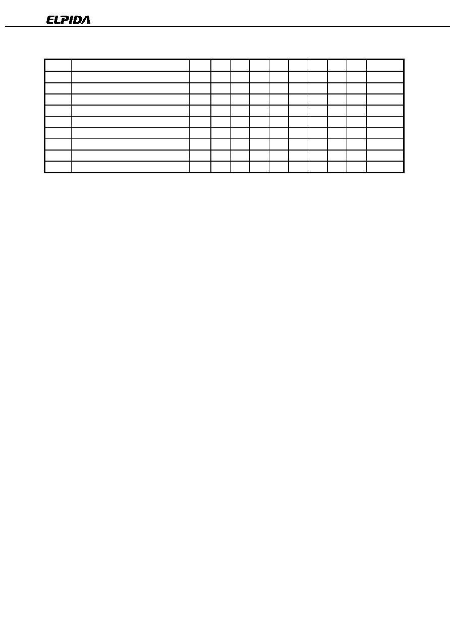
(2/2)
Byte No.
Function Described
Hex
Bit 7 Bit 6 Bit 5 Bit 4 Bit 3 Bit 2 Bit 1 Bit 0
Notes
65-71
Manufacture's
JEDEC
ID
code
72
Manufacturing
location
73-90
Manufacture's
P/N
91-92
Revision
code
93-94
Manufacturing
date
95-98
Assembly
serial
number
99-125
Mfg
specific
126
Intel
specification
frequency
64H 0 1 1 0 0 1 0 0
100MHz
127
Intel
specification
/CAS
latency
support FFH 1 1 1 1 1 1 1 1
Timing Chart
Refer to the
�
�
�
�
PD45128441, 45128841, 45128163 Data sheet (E0031N).
12
MC-4532CD647XFA
Data Sheet E0230N20 (Ver. 2.0)
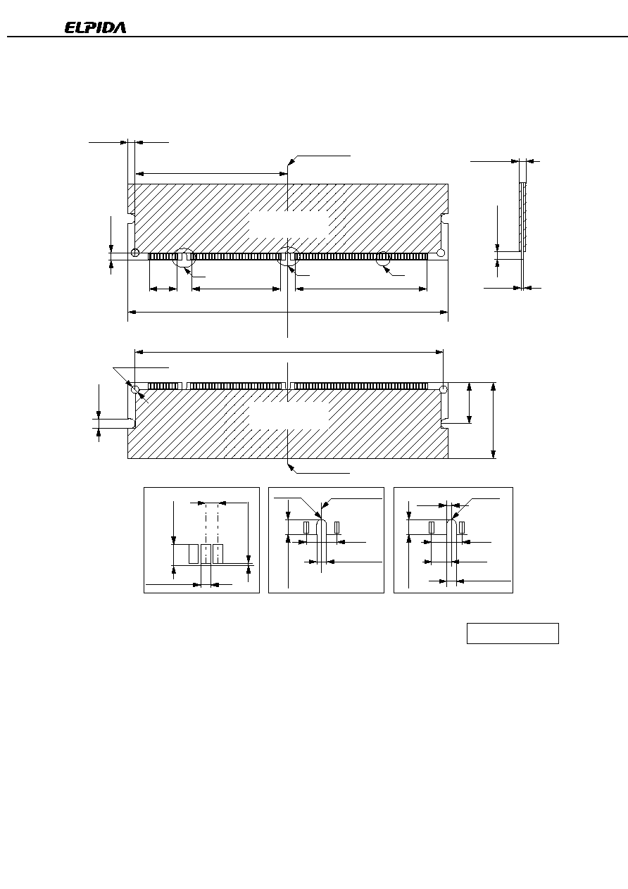
Package Drawing
6.35
6.35
1.00
Detail B
Detail C
Detail A
0.20 � 0.15
2.50 � 0.20
1.27
0.050
3.00
133.35
3.00
11.43
36.83
54.61
(63.67)
A
B
C
1
84
Front side
Back side
85
4.00
17.80
34.93
168
2 �
3.00
1.00 � 0.05
2.00 � 0.10
4.175
2.00 � 0.10
(DATUM -A-)
(DATUM -A-)
Unit: mm
(DATUM -A-)
R FULL
R FULL
Note: Tolerance on all dimensions � 0.15 unless otherwise specified.
127.35
Component area
(Front)
Component area
(Back)
1.27
4.00 Min
4.80 Max
3.125 � 0.125
3.125 � 0.125
ECA-TS2-0049-01
13
MC-4532CD647XFA
Data Sheet E0230N20 (Ver. 2.0)
CAUTION FOR HANDLING MEMORY MODULES
When handling or inserting memory modules, be sure not to touch any components on the modules, such as
the memory ICs, chip capacitors and chip resistors. It is necessary to avoid undue mechanical stress on
these components to prevent damaging them.
In particular, do not push module cover or drop the modules in order to protect from mechanical defects,
which would be electrical defects.
When re-packing memory modules, be sure the modules are not touching each other.
Modules in contact with other modules may cause excessive mechanical stress, which may damage the
modules.
MDE0202
NOTES FOR CMOS DEVICES
1
PRECAUTION AGAINST ESD FOR MOS DEVICES
Exposing the MOS devices to a strong electric field can cause destruction of the gate
oxide and ultimately degrade the MOS devices operation. Steps must be taken to stop
generation of static electricity as much as possible, and quickly dissipate it, when once
it has occurred. Environmental control must be adequate. When it is dry, humidifier
should be used. It is recommended to avoid using insulators that easily build static
electricity. MOS devices must be stored and transported in an anti-static container,
static shielding bag or conductive material. All test and measurement tools including
work bench and floor should be grounded. The operator should be grounded using
wrist strap. MOS devices must not be touched with bare hands. Similar precautions
need to be taken for PW boards with semiconductor MOS devices on it.
2
HANDLING OF UNUSED INPUT PINS FOR CMOS DEVICES
No connection for CMOS devices input pins can be a cause of malfunction. If no
connection is provided to the input pins, it is possible that an internal input level may be
generated due to noise, etc., hence causing malfunction. CMOS devices behave
differently than Bipolar or NMOS devices. Input levels of CMOS devices must be fixed
high or low by using a pull-up or pull-down circuitry. Each unused pin should be connected
to V
DD
or GND with a resistor, if it is considered to have a possibility of being an output
pin. The unused pins must be handled in accordance with the related specifications.
3
STATUS BEFORE INITIALIZATION OF MOS DEVICES
Power-on does not necessarily define initial status of MOS devices. Production process
of MOS does not define the initial operation status of the device. Immediately after the
power source is turned ON, the MOS devices with reset function have not yet been
initialized. Hence, power-on does not guarantee output pin levels, I/O settings or
contents of registers. MOS devices are not initialized until the reset signal is received.
Reset operation must be executed immediately after power-on for MOS devices having
reset function.
CME0107

MC-4532CD647XFA
M01E0107
No part of this document may be copied or reproduced in any form or by any means without the prior
written consent of Elpida Memory, Inc.
Elpida Memory, Inc. does not assume any liability for infringement of any intellectual property rights
(including but not limited to patents, copyrights, and circuit layout licenses) of Elpida Memory, Inc. or
third parties by or arising from the use of the products or information listed in this document. No license,
express, implied or otherwise, is granted under any patents, copyrights or other intellectual property
rights of Elpida Memory, Inc. or others.
Descriptions of circuits, software and other related information in this document are provided for
illustrative purposes in semiconductor product operation and application examples. The incorporation of
these circuits, software and information in the design of the customer's equipment shall be done under
the full responsibility of the customer. Elpida Memory, Inc. assumes no responsibility for any losses
incurred by customers or third parties arising from the use of these circuits, software and information.
[Product applications]
Elpida Memory, Inc. makes every attempt to ensure that its products are of high quality and reliability.
However, users are instructed to contact Elpida Memory's sales office before using the product in
aerospace, aeronautics, nuclear power, combustion control, transportation, traffic, safety equipment,
medical equipment for life support, or other such application in which especially high quality and
reliability is demanded or where its failure or malfunction may directly threaten human life or cause risk
of bodily injury.
[Product usage]
Design your application so that the product is used within the ranges and conditions guaranteed by
Elpida Memory, Inc., including the maximum ratings, operating supply voltage range, heat radiation
characteristics, installation conditions and other related characteristics. Elpida Memory, Inc. bears no
responsibility for failure or damage when the product is used beyond the guaranteed ranges and
conditions. Even within the guaranteed ranges and conditions, consider normally foreseeable failure
rates or failure modes in semiconductor devices and employ systemic measures such as fail-safes, so
that the equipment incorporating Elpida Memory, Inc. products does not cause bodily injury, fire or other
consequential damage due to the operation of the Elpida Memory, Inc. product.
[Usage environment]
This product is not designed to be resistant to electromagnetic waves or radiation. This product must be
used in a non-condensing environment.
If you export the products or technology described in this document that are controlled by the Foreign
Exchange and Foreign Trade Law of Japan, you must follow the necessary procedures in accordance
with the relevant laws and regulations of Japan. Also, if you export products/technology controlled by
U.S. export control regulations, or another country's export control laws or regulations, you must follow
the necessary procedures in accordance with such laws or regulations.
If these products/technology are sold, leased, or transferred to a third party, or a third party is granted
license to use these products, that third party must be made aware that they are responsible for
compliance with the relevant laws and regulations.
The information in this document is subject to change without notice. Before using this document, confirm that this is the latest version.