The information in this document is subject to change without notice. Before using this document, please
confirm that this is the latest version.
Not all devices/types available in every country. Please check with local Elpida Memory, Inc. for
availability and additional information.
MOS INTEGRATED CIRCUIT
µ
µ
µ
µ
PD45128441, 45128841, 45128163
128M-bit Synchronous DRAM
4-bank, LVTTL
DATA SHEET
Document No. E0031N30 (Ver. 3.0)
Date Published August 2001 CP (K)
Printed in Japan
Elpida Memory, Inc. is a joint venture DRAM company of NEC Corporation and Hitachi, Ltd.
Description
The
µ
PD45128441, 45128841, 45128163 are high-speed 134,217,728-bit synchronous dynamic random-access
memories, organized as 8,388,608
◊
4
◊
4, 4,194,304
◊
8
◊
4, 2,097,152
◊
16
◊
4 (word
◊
bit
◊
bank), respectively.
The synchronous DRAMs achieved high-speed data transfer using the pipeline architecture.
All inputs and outputs are synchronized with the positive edge of the clock.
The synchronous DRAMs are compatible with Low Voltage TTL (LVTTL).
These products are packaged in 54-pin TSOP (II).
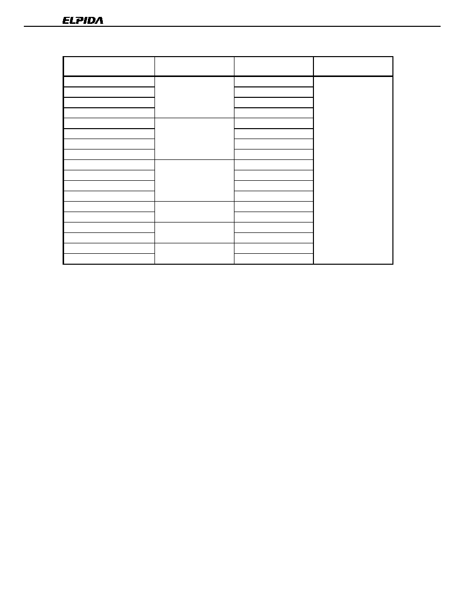
Features
∑
Fully Synchronous Dynamic RAM, with all signals referenced to a positive clock edge
∑
Pulsed interface
∑
Possible to assert random column address in every cycle
∑
Quad internal banks controlled by BA0(A13) and BA1(A12)
∑
Byte control (
◊
16) by LDQM and UDQM
∑
Programmable Wrap sequence (Sequential / Interleave)
∑
Programmable burst length (1, 2, 4, 8 and full page)
∑
Programmable /CAS latency (2 and 3)
∑
Automatic precharge and controlled precharge
∑
CBR (Auto) refresh and self refresh
∑
◊
4,
◊
8,
◊
16 organization
∑
Single 3.3 V
±
0.3 V power supply
∑
LVTTL compatible inputs and outputs
∑
4,096 refresh cycles / 64 ms
∑
Burst termination by Burst stop command and Precharge command
Data Sheet E0031N30
4
µ
µ
µ
µ
PD45128441, 45128841, 45128163
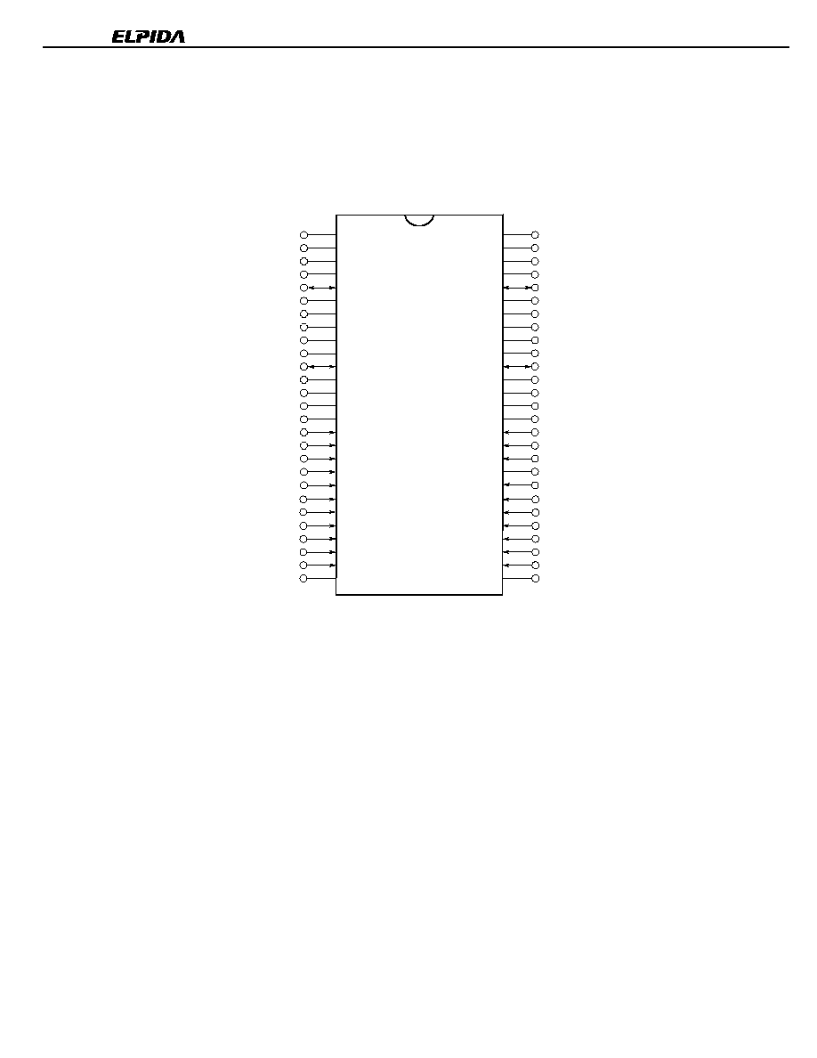
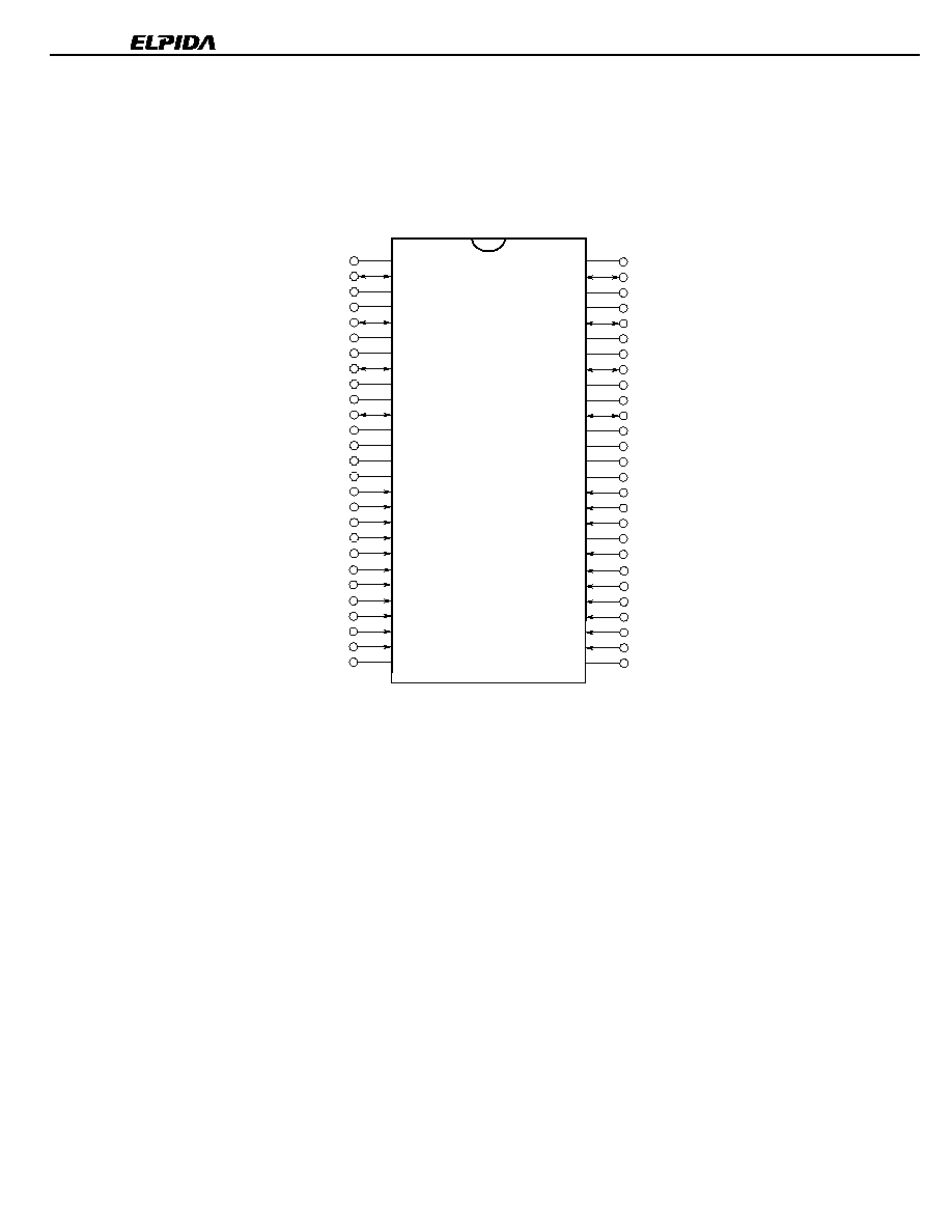
Pin Configurations
/xxx indicates active low signal.
[
µ
µ
µ
µ
PD45128441]
54-pin Plastic TSOP (II) (10.16mm (400))
8M words
◊
◊
◊
◊
4 bits
◊
◊
◊
◊
4 banks
V
CC
NC
V
CC
Q
NC
DQ0
V
SS
Q
NC
NC
V
CC
Q
NC
DQ1
V
SS
Q
NC
V
CC
NC
/WE
/CAS
/RAS
/CS
BA0(A13)
BA1(A12)
A10
A0
A1
A2
A3
V
CC
1
2
3
4
5
6
7
8
9
10
11
12
13
14
15
16
17
18
19
20
21
22
23
24
25
26
27
Vss
NC
VssQ
NC
DQ3
VccQ
NC
NC
VssQ
NC
DQ2
VccQ
NC
Vss
NC
DQM
CLK
CKE
NC
A11
A9
A8
A7
A6
A5
A4
Vss
54
53
52
51
50
49
48
47
46
45
44
43
42
41
40
39
38
37
36
35
34
33
32
31
30
29
28
A0 to A11
Note
:
Address
inputs
BA0(A13), BA1(A12) : Bank select
DQ0 to DQ3
: Data inputs / outputs
CLK :
Clock
input
CKE :
Clock
enable
/CS :
Chip
select
/RAS
: Row address strobe
/CAS
: Column address strobe
/WE
: Write enable
DQM
: DQ mask enable
V
CC
: Supply voltage
V
SS
:
Ground
V
CC
Q
: Supply voltage for DQ
V
SS
Q
: Ground for DQ
NC
: No connection
Note A0 to A11
: Row address inputs
A0 to A9, A11 : Column address inputs
Data Sheet E0031N30
5
µ
µ
µ
µ
PD45128441, 45128841, 45128163
[
µ
µ
µ
µ
PD45128841]
54-pin Plastic TSOP (II) (10.16mm (400))
4M words
◊
◊
◊
◊
8 bits
◊
◊
◊
◊
4 banks
V
CC
DQ0
V
CC
Q
NC
DQ1
V
SS
Q
NC
DQ2
V
CC
Q
NC
DQ3
V
SS
Q
NC
V
CC
NC
/WE
/CAS
/RAS
/CS
BA0(A13)
BA1(A12)
A10
A0
A1
A2
A3
V
CC
Vss
DQ7
VssQ
NC
DQ6
VccQ
NC
DQ5
VssQ
NC
DQ4
VccQ
NC
Vss
NC
DQM
CLK
CKE
NC
A11
A9
A8
A7
A6
A5
A4
Vss
1
2
3
4
5
6
7
8
9
10
11
12
13
14
15
16
17
18
19
20
21
22
23
24
25
26
27
54
53
52
51
50
49
48
47
46
45
44
43
42
41
40
39
38
37
36
35
34
33
32
31
30
29
28
A0 to A11
Note
:
Address
inputs
BA0(A13), BA1(A12) : Bank select
DQ0 to DQ7
: Data inputs / outputs
CLK :
Clock
input
CKE :
Clock
enable
/CS :
Chip
select
/RAS
: Row address strobe
/CAS
: Column address strobe
/WE
: Write enable
DQM
: DQ mask enable
V
CC
: Supply voltage
V
SS
:
Ground
V
CC
Q
: Supply voltage for DQ
V
SS
Q
: Ground for DQ
NC
: No connection
Note A0 to A11 : Row address inputs
A0 to A9 : Column address inputs