
ELAN MICROELECTRONICS CORP.
No. 12, Innovation 1
st
RD., Science-Based Industrial Park
Hsin Chu City, Taiwan, R.O.C.
TEL: (03) 5639977
FAX: (03) 5630118
EM78569
8-BIT MICRO-CONTROLLER
Version 4.0

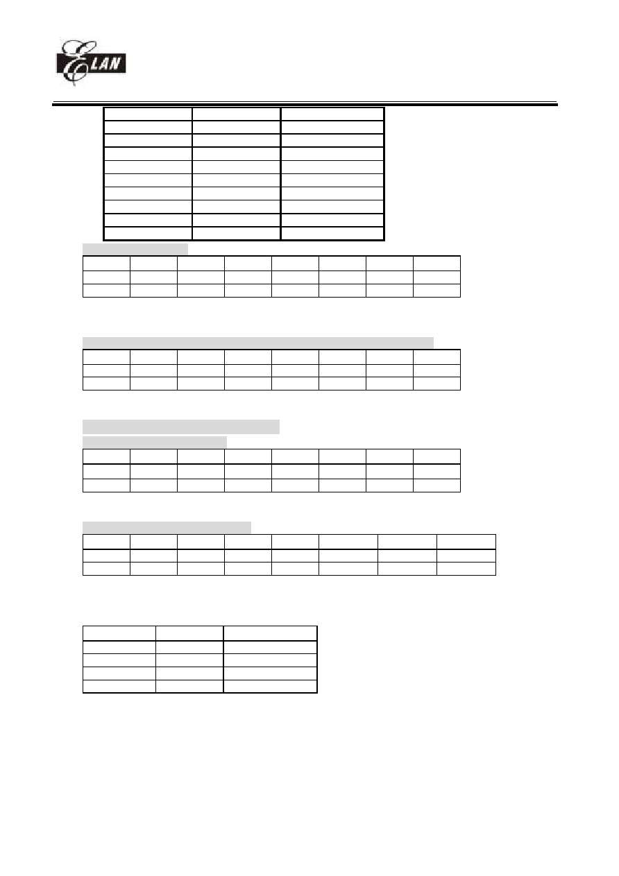
Version History
Specification Revision History
Version Content
Release
Date
EM78569
1.0 Initial
version
2002/06/10
3.1
Modify Multiplier architecture
2003/3/10
3.2
1. Move DARES bit from bit7 to bit3.
2. Change instruction "MUL" "INT A"
3. Modify
Sink/Driver
current
2003/5/2
3.3
1. Update Application Note
2. Add 17.91MHz main CLK
2003/6/9
3.4
1. Add data RAM address auto-increase function
2. Add mclk/2 signal output. (output shared with PC0)
3. Add carry bit calculation function.(ADD, SUB)
2003/8/1
3.5
1. Modify code option define.
2003/9/17
3.6
1. ADD the description about ADC's offset voltage
2003/10/22
3.7
1. Decrease stack from 16 to 12
2. Modify the operating temperature
3. Modify Port9 sink/driver current
2004/4/10
3.8
Add the OSC stable and reset timing diagram
2004/7/2
3.9
Modify Normal mode power consumption
2004/8/19
4.0 Remove
IDLE
mode
Modify operating temperature
2004/8/31
User Application Note
(Before using this chip, take a look at the following description note, it includes important messages.)
1. There are some undefined bits in the registers. The values in these bits are unpredicted. These bits are not allowed to
use. We use the symbol "-" in the spec to recognize them.
2. You will see some names for the register bits definitions. Some name will be appear very frequently in the whole spec.
The following describes the meaning for the register's definitions such as bit type, bit name, bit number and so on.
7
6
5
4
3
2
1
0
RAB7
RAB6
BAB5
RAB4
RAB2
RAB0
R/W -0
R/W -0
R-1
R/W -1
R
R/W
Bit type
Bit name
Bit number
read/write
(default value=0)
read/write
(default value=1)
read only
(w/o default value)
read/write
(w/o default value)
PAGE0
RA
Register name and its page
-
RAB1
(undefined) not allowed to use
R-0
read only
(default value=0)
read only
(default value=1)
3. Please set 1 to RA page2 bit7 or LCD waveform will difference between mask and romless.
4. Please set IOCC PAGE1 bit0 to "1" otherwise partial ADC function cannot be used
5. For 8 bits resolution DAC, DAO pin will output corresponding voltage after write new data to DAC data buffer(RA
PAGE1). For 10 bits resolution, DAO pin will output constant after change DAC most significant 2 bits (R5 PAGE1
bit6~7). DAO will output correct voltage after write data to least significant 8 bits. That is to say, when using 10 bits
resolution DAC, user must write most significant 2 bits and least significant 8 bits in order.
6. Base on "VERSEL"(code option) equal 0 or 1, R8 page1 and RB page2's define are different.
"VERSEL" = 0: R8 page1 defined to data RAM address buffer
RB page2 defined to multiplier's Y data or Y address buffer (controlled by RA page2 bit5 "INDR").

EM78569
8-bit Micro-controller
__________________________________________________________________________________________________________________________________________________________________
* This specification is subject to be changed without notice.
1
8/31/2004 (V4.0)
RA page2 bit4(PLUS) determine RAM address auto increase or not (only for multiplier's addressing).
RA page2 bit7 is undefined.
"VERSEL" = 1: R8 page1 is undefined.
RA page2 bit4(PLUS) determine RAM address auto increase or not (for data RAM and multiplier's
addressing).
RA page2 bit7(INS) determine .
RB page2 defined to multiplier's Y data, Y address or data RAM address buffer.
7. The carry bit's initial value is un-know, please define the initial value before execute first ADD or SUB instruction that
include carry bit.(VERSEL =1 and INS = 1)
8. In EM78569's developing tool, "VERSEL" and "PHO" are at RD page2 bit6 and bit5, but in mask chip, these two bits
will mapping to code option. Please set these two bits to fixed value at initial and do not change these two bit
among your program.
9. While switching main clock (regardless of high freq to low freq or on the other hand), adding 6 instructions delay (NOP)
is required.
10. Please do not switch MCU operation mode from normal mode to sleep mode directly. Before into sleep mode, please
switch MCU to green mode.
11. Offset voltage will effect ADC's result, please refer to figure 20 to detail.
The differences between ICE569, EM78P569 and EM78569.
ICE569 EM78P569
EM78569
Stack 16
16
12
VERSEL, PHO
RD page0 bit5,6
Code option
Code option

EM78569
8-bit Micro-controller
__________________________________________________________________________________________________________________________________________________________________
* This specification is subject to be changed without notice.
2
8/31/2004 (V4.0)
I. General Description
The EM78569 is an 8-bit RISC type microprocessor with low power, high speed CMOS technology. This
integrated single chip has an on_chip watchdog timer (WDT), program ROM, data RAM, LCD driver, programmable
real time clock/counter, internal interrupt, power down mode, built-in three-wire SPI, dual PWM(Pulse Width
Modulation), 10-bit A/D converter, 10-bit DA converter and tri-state I/O.
II. Feature
CPU
�
Operating voltage : 2.2V~5.5V at main CLK less then 3.58MHz.
Main CLK(Hz)
Under 3.58M
7.16M
10.74M
14.4M
17.9M
Operating Voltage(min)
2.2
2.5
3
3.6
4V
�
16k x 13 on chip Program ROM.
�
1k x 8 on chip data RAM
�
Up to 51 bi-directional tri-state I/O ports(22 pin shared with LCD)
�
12 level stack for subroutine nesting
�
8-bit real time clock/counter (TCC)
�
Two 8-bit counters : COUNTER1 and COUNTER2
�
On-chip watchdog timer (WDT)
�
99.9 single instruction cycle commands
�
Three modes (Main clock can be programmed from 447.829k to 17.9MHz generated by internal PLL)
Mode
CPU status
Main clock
32.768kHz clock status
Sleep mode
Turn off
Turn off
Turn off
Green mode
Turn on
Turn off
Turn on
Normal mode
Turn on
Turn on
Turn on
�
8 level Normal mode frequency : 447.8K , 895.7K , 1.79M , 3.58M , 7.16M , 10.75M , 14.3M , 17.9MHz.
�
Input port interrupt function
�
10 interrupt source , 4 external , 6 internal
�
Dual clocks operation (Internal PLL main clock , External 32.768KHz)
SPI
�
Serial Peripheral Interface (SPI) : a kind of serial I/O interface
�
Interrupt flag available for the read buffer full or transmitter buffer empty.
�
Programmable baud rates of communication
�
Three-wire synchronous communication. (shared with IO)
PWM
�
Dual PWM (Pulse Width Modulation) with 10-bit resolution
�
Programmable period (or baud rate)
�
Programmable duty cycle
ADC
�
Operating : 2.5V5.5V
�
6 channel 10-bit successive approximation A/D converter
�
Internal (VDD) or external reference
DAC
�
Operating : 2.5V5.5V under VDD reference, 2.8V ~ 5.5V under 2.5V reference
�
10-bit R-2R D/A converter
�
Internal (VDD or 2.5V) reference
POR
�
2.0V Power-on voltage detector reset
Build-in LCD driver(4 X 32)
�
Common driver pins : 4
�
Segment driver pins : 32

EM78569
8-bit Micro-controller
__________________________________________________________________________________________________________________________________________________________________
* This specification is subject to be changed without notice.
3
8/31/2004 (V4.0)
�
1/3 bias
�
1/4 duty, 1/2 duty
�
16 Level LCD contrast control by software
Multiplication
�
8 x 8 multiplication
PACKAGE
�
73-pin die or 100-pin QFP
III. Application
Communication or general product.
IV. Pin Configuration
NC
NC
NC
NC
NC
NC
NC
NC
1
2
3
4
5
6
7
8
9
10
11
12
13
14
15
16
17
18
21
22
24
25
27
28
29
30
50
49
48
47
46
45
44
43
42
41
40
39
38
37
36
35
75
74
73
70
69
68
67
66
65
64
63
62
61
60
59
58
57
56
55
54
53
52
51
NC
20
26
SEG21/PB7
33
34
19
23
31
32
AD
3/
P62
AD
2/
P61
AD
1/
P60
P87
72
71
SEG
13/
P97
SEG
12/
P57
SEG
11/
P56
SEG
1
0/
P55
82
83
84
85
86
87
88
89
90
91
92
93
94
95
96
97
98
99
10
0
81
SEG
14/
P96
SEG
15/
P95
SEG23/PB5
SEG24/PB4
SEG25/PB3
SEG26/PB2
SEG27/PB1
SEG28/PB0
SEG29/PC7
SEG30/PC6
SEG31/PC5
PC4
PC3
PWM2/PC2
PWM1/PC1
PC0
SEG22/PB6
COM3
COM2
COM1
COM0
SEG
1
SEG0
SEG
9
SEG
8
SEG
7
SEG
6
SEG
5
SEG
4
SEG
3
SEG
2
DA
O/
P
6
7
VR
E
F
/
P
6
6
AD
6/
P65
AD
5/
P64
AD
4/
P63
P86
P85
XI
N
XOUT
VS
S
P84
P83
P82
NC
NC
NC
NC
NC
NC
80
79
78
SEG
16/
P94
77
76
SEG
18/
P92
SEG
19/
P91
SEG
20/
P90
SEG
17/
P93
P77
SCK/P76
SDO/P75
SDI/P74
INT3/P73
INT2/P72
INT1/P71
INT0/P70
VDD
P81
P80
AVDD
NC
NC
NC
NC
PLLC
NC
NC
NC
NC
NC
NC
NC
NC
/
R
ESET
AVSS
Fig 1 : 74-pin die or 100-pin QFP

EM78569
8-bit Micro-controller
__________________________________________________________________________________________________________________________________________________________________
* This specification is subject to be changed without notice.
4
8/31/2004 (V4.0)
V. Functional Block Diagram
TIMING
CONTROL
TIMER
TCC
COUNTER1
COUNTER2
WDT
ROM
DATA RAM
CONTROL REGISTER
LCD DRIVER
I/O PORT
CPU
SPI
PWM
10-bit A/D
RAM
10-bit D/A
Fig.2a Block diagram
XIN
PLLC
Oscillator
timing control
R1(TCC)
Prescaler
WDT
timer
General
RAM
R4
Interrupt
control
Instruction
decoder
Instruction
register
ROM
R3
R5
ACC
ALU
STACK
DATA & Control Bus
XOUT
R2
DATA
RAM
Control sleep
and wakeup
on I/O port
P55~P57
SPI
PWM
10-bit A/D
IOC5
R5
PORT5
P60~P67
IOC6
R6
PORT6
P70~P77
IOC7
R7
PORT7
P80~P87
IOC8
R8
PORT8
P90~P97
IOC9
R9
PORT9
PB0~PB7
IOCB
RB
PORTB
PC0~PC7
IOCC
RC
PORTC
LCD RAM
LCD driver
COM0~COM3
SEG0~SEG31
10-bit D/A
Fig.2b Block diagram

EM78569
8-bit Micro-controller
__________________________________________________________________________________________________________________________________________________________________
* This specification is subject to be changed without notice.
5
8/31/2004 (V4.0)
VI. Pin Descriptions
PIN I/O DESCRIPTION
POWER
VDD
AVDD
POWER Digital
power
Analog power
VSS
AVSS
POWER Digital
ground
Analog ground
CLOCK
XIN
I
Input pin for 32.768 kHz oscillator
XOUT
O
Output pin for 32.768 kHz oscillator
PLLC
I
Phase loop lock capacitor, connect a capacitor 0.01u to 0.047u to the ground.
LCD
COM0 ~ COM3 O
Common driver pins of LCD drivers
SEG0 ~ SEG9
SEG10 ~ SEG12
SEG13 ~ SEG20
SEG21 ~ SEG28
SEG29 ~ SEG31
O
O (I/O : PORT5)
O (I/O : PORT9)
O (I/O : PORTB)
O (I/O : PORTC)
Segment driver pins of LCD drivers
SEG10 to SEG31 are shared with IO PORT.
10-bit 6 channel A/D
VREF
I (P66)
ADC reference input. Shared with PORT66
AD1
I (P60)
ADC input channel 1. Shared with PORT60()
AD2
I (P61)
ADC input channel 2. Shared with PORT61
AD3
I (P62)
ADC input channel 3. Shared with PORT62
AD4
I (P63)
ADC input channel 4. Shared with PORT63
AD5
I(P64)
ADC input channel 5. Shared with PORT64
AD6
I(P65)
ADC input channel 6. Shared with PORT65
10-bit D/A
DAO
O(P67)
DAO is 10 bit DA output shared with PORT67
SPI
SCK
IO (PORT76)
Master: output pin, Slave: input pin. This pin shared with PORT76.
SDO
O (PORT75)
Output pin for serial data transferring. This pin shared with PORT75.
SDI
I (PORT74)
Input pin for receiving data. This pin shared with PORT74.
PWM
PWM1
O
Pulse width modulation output channel 1
PWM2
O
Pulse width modulation output channel 2
IO
P55~P57
I/O
PORT5 can be INPUT or OUTPUT port each bit.
PORT5(7:5) are shared with LCD Segment signal.
P60 ~P67
I/O
PORT6 can be INPUT or OUTPUT port each bit.
P70 ~ P77
I/O
PORT7 can be INPUT or OUTPUT port each bit.
PORT7(4~6) are shared with SPI interface pins
Internal Pull high function.
Interrupt function.
P80 ~ P87
I/O
PORT8 can be INPUT or OUTPUT port each bit.
Internal pull high.
PORT85 ~ P87 are shared with ADC input
PORT8(0~3) have wake-up functions(set by RE PAGE0)

EM78569
8-bit Micro-controller
__________________________________________________________________________________________________________________________________________________________________
* This specification is subject to be changed without notice.
6
8/31/2004 (V4.0)
P90 ~ P97
I/O
PORT9 can be INPUT or OUTPUT port each bit.
PORT9 are shared with LCD Segment signal.
PB0 ~ PB7
I/O
PORTB can be INPUT or OUTPUT port each bit.
PORTB are shared with LCD Segment signal.
PC0 ~ PC7
I/O
PORTC can be INPUT or OUTPUT port each bit.
PORTC(7:5) are shared with LCD Segment signal.
INT0
PORT70
Interrupt sources. Once PORT70 has a falling edge or rising edge signal
(controlled by CONT register), it will generate a interruption.
INT1
PORT71
Interrupt sources which has the same interrupt flag. Any pin from PORT71
has a falling edge signal, it will generate a interruption.
INT2
PORT72
Interrupt sources which has the same interrupt flag. Any pin from PORT72
has a falling edge signal, it will generate a interruption.
INT3
PORT73
Interrupt sources which has the same interrupt flag. Any pin from PORT73
has a falling edge signal, it will generate a interruption.
/RESET I
Low
reset

EM78569
8-bit Micro-controller
__________________________________________________________________________________________________________________________________________________________________
* This specification is subject to be changed without notice.
7
8/31/2004 (V4.0)
VII. Functional Descriptions
VII.1 Operational Registers
Register configuration
R
PAGE
registers
Addr R PAGE0
R PAGE1
R PAGE2
R PAGE3
00 Indirect
addressing
01 TCC
02 PC
03 Page,
Status
04 RAM bank, RSR
05 Port5 I/O data,
Program ROM page
LCD RAM address SPI control
PWM control
06 Port6 I/O data
LCD data buffer
SPI data buffer
Duty of PWM1
07 Port7 I/O data
Data RAM bank
PWM1 control
Duty of PWM1
08 Port8 I/O data
Data RAM address
Period of PWM1
09 Port9 I/O data
Data RAM data
buffer
Duty
of
PWM2
0A PLL, Main clock,
WDTE
DAC input data
buffer
Multiplier control
PWM2 control
Duty of PWM2
0B PortB I/O data
ADC output data
buffer
Multiplicant Y
Period of PWM2
0C PortC I/O data
Counter1 data
MR(0~7)
0D LCD
control
Counter2
data
MR(8~15)
0E Wake-up
control,
Interrupt flag
MR(16~23)
0F Interrupt
flag
10 16
bytes
: Common
registers
1F
20 Bank0~Bank3
: Common
registers
3F (32x8 for each
bank)
IOC
PAGE
registers
Addr IOC PAGE0
IOC PAGE1
00
01
02
03
04
05 Port5
I/O
control,
LCD bias control
06 Port6 I/O control
Port6 switches
07 Port7 I/O control
Port7 pull high
08 Port8 I/O control
Port8 pull high
09 Port9 I/O control
Port9 switches
0A
DAC
control
0B PortB I/O control
ADC control
0C PortC I/O control
Port5,8,B,C switch
0D
Clock

EM78569
8-bit Micro-controller
__________________________________________________________________________________________________________________________________________________________________
* This specification is subject to be changed without notice.
8
8/31/2004 (V4.0)
source(CN1,CN2)
Prescaler(CN1,CN2
)
0E Interrupt
mask
0F Interrupt
mask
10
:
1F
20
:
3F
VII.2 Operational Register Detail Description
R0 (Indirect Addressing Register)
R0 is not a physically implemented register. It is used as indirect addressing pointer. Any instruction using R0
as register actually accesses data pointed by the RAM Select Register (R4).
Example:
Mov A, @0x20
;store a address at R4 for indirect addressing
Mov 0x04,
A
Mov A, @0xAA
;write data 0xAA to R20 at bank0 through R0
Mov 0x00,
A
R1 (TCC)
TCC data buffer. Increased by 16.384KHz or by the instruction cycle clock (controlled by CONT register).
Written and read by the program as any other register.
R2 (Program Counter)
The structure is depicted in Fig.3.
Generates 16k
� 13 external ROM addresses to the relative programming instruction codes.
"JMP" instruction allows the direct loading of the low 10 program counter bits.
"CALL" instruction loads the low 10 bits of the PC, PC+1, and then push into the stack.
"RET'' ("RETL k", "RETI") instruction loads the program counter with the contents at the top of stack.
"MOV R2, A" allows the loading of an address from the A register to the PC, and the ninth and tenth bits are
cleared to "0''.
"ADD R2,A" allows a relative address be added to the current PC, and contents of the ninth and tenth bits are
cleared to "0''.
"TBL" allows a relative address added to the current PC, and contents of the ninth and tenth bits don't change.
The most significant bit (A10~A13) will be loaded with the contents of bit PS0~PS3 in the status register (R5
PAGE0) upon the execution of a "JMP'', "CALL'', "ADD R2, A'', or "MOV R2, A'' instruction.
If an interrupt is triggered, PROGRAM ROM will jump to address 0x08 at page0. The CPU will store ACC,
R3 status and R5 PAGE automatically, and they will be restored after instruction RETI.

EM78569
8-bit Micro-controller
__________________________________________________________________________________________________________________________________________________________________
* This specification is subject to be changed without notice.
9
8/31/2004 (V4.0)
Fig.3 Program counter organization
R3 (Status, Page selection)
(Status flag, Page selection bits)
7
6
5 4 3 2 1 0
RPAGE1 RPAGE0 IOCPAGE
T P Z DC C
R/W-0 R/W-0 R/W-0 R R R/W
R/W
R/W
Bit 0(C) : Carry flag
Bit 1(DC) : Auxiliary carry flag
Bit 2(Z) : Zero flag
Bit 3(P) : Power down bit
Set to 1 during power on or by a "WDTC" command and reset to 0 by a "SLEP" command.
Bit 4(T) : Time-out bit
Set to 1 by the "SLEP" and "WDTC" command, or during power up and reset to 0 by WDT timeout.
EVENT T
P
REMARK
WDT wake up from sleep mode
0
0
WDT time out (not sleep mode)
0
1
/RESET wake up from sleep
1
0
Power up
1
1
Low pulse on /RESET
x
X
x : don't care
Bit 5(IOCPAGE) : change IOC5 ~ IOCE to another page
Please refer to Fig.4 control register configuration for details.
0/1 IOC page0 / IOC page1
Bit 6(RPAGE0 ~ RPAGE1) : change R5 ~ RE to another page
Please refer to VII.1 Operational registers for detail register configuration.
(RPAGE1,RPAGE0)
R page # selected
(0,0) R
page
0
(0,1) R
page
1
(1,0) R
page
2
(1,1) R
page
3
PC
A13 A12 A11 A10 A9 A8 A7~A0
0000
PAGE0 0000~03FF
0001
PAGE1 0400~07FF
1110
PAGE14 3800~3BFF
1111
PAGE15 3C00~3FFF
0010
PAGE2 0800~0BFF
STACK1
STACK2
STACK3
STACK4
STACK5
STACK6
STACK7
STACK8
STACK9
STACK10
STACK11
STACK12
STACK13
STACK14
STACK15
STACK16
CALL and
INTERRUPT
RET
RETL
RETI
ACC,R3,R5(PAGE)
R5(PAGE)
store
restore

EM78569
8-bit Micro-controller
__________________________________________________________________________________________________________________________________________________________________
* This specification is subject to be changed without notice.
10
8/31/2004 (V4.0)
R4 (RAM selection for common registers R20 ~ R3F))
(RAM selection register)
7 6 5 4 3 2 1 0
RB1 RB0 RSR5 RSR4 RSR3 RSR2 RSR1 RSR0
R/W-0
R/W-0 R/W R/W R/W R/W R/W R/W
Bit 0 ~ Bit 5 (RSR0 ~ RSR5) : Indirect addressing for common registers R20 ~ R3F
RSR bits are used to select up to 32 registers (R20 to R3F) in the indirect addressing mode.
Bit 6 ~ Bit 7 (RB0 ~ RB1) : Bank selection bits for common registers R20 ~ R3F
These selection bits are used to determine which bank is activated among the 4 banks for 32 register (R20 to
R3F)..
Please refer to VII.1 Operational registers for details.
R5 (PORT5 I/O data, Program page selection, LCD address, SPI control)
PAGE0 (PORT5 I/O data register, Program page register)
7 6 5 4 3 2 1 0
P57 P56 P55 - PS3 PS2 PS1 PS0
R/W R/W R/W
R/W-0 R/W-0 R/W-0 R/W-0
Bit 0 ~ Bit 3 (PS0 ~ PS3) : Program page selection bits
PS3 PS2 PS1
PS0 Program
memory page (Address)
0 0 0 0
Page
0
0 0 0 1
Page
1
0 0 1 0
Page
2
0 0 1 1
Page
3
: : : :
:
: : : :
:
1 1 1 0
Page
14
1 1 1 1
Page
15
User can use PAGE instruction to change page to maintain program page by user. Otherwise, user can use
far jump (FJMP) or far call (FCALL) instructions to program user's code. And the program page is
maintained by EMC's complier. It will change user's program by inserting instructions within program.
Bit 4 : unused
Bit 5 ~ Bit 7 (P55 ~ P57) : 8-bit PORT5(5~7) I/O data register
User can use IOC register to define input or output each bit.
PAGE1 (LCD address)
7 6 5 4 3 2 1 0
DA9 DA8 - -
LCDA3
LCDA2
LCDA1
LCDA0
R/W-0 R/W-0
R/W-0 R/W-0 R/W-0 R/W-0
Bit 0 ~ Bit 3 (LCDA0 ~ LCDA3) : LCD address for LCD RAM read or write
The address of the LCD RAM correspond to the COMMON and SEGMENT signals as the table.
COM3 ~ COM0
LCD address
(LCDA3 ~ LCDA0)
SEG1, SEG0
00H
SEG3, SEG2
01H
SEG5, SEG4
02H
SEG7, SEG6
03H
SEG9, SEG8
04H
SEG11, SEG10
05H
SEG13, SEG12
06H
SEG15, SEG14
07H

EM78569
8-bit Micro-controller
__________________________________________________________________________________________________________________________________________________________________
* This specification is subject to be changed without notice.
11
8/31/2004 (V4.0)
SEG17, SEG16
08H
SEG19, SEG18
09H
SEG21, SEG20
0AH
SEG23, SEG22
0BH
SEG25, SEG24
0CH
SEG27, SEG26
0DH
SEG29, SEG28
0EH
SEG31, SEG30
0FH
Bit 4 ~ Bit 5 : unused
Bit 6 ~ Bit 7(DA8~DA9) : DA8 and DA9 are DAC MSB when R7 page1 bit 3(DARES) is set ,.or unused
when DAREF clear to 0. When using 10 bits resolution DAC, DAO output voltage will
unchanged after write data to these two bits. DAO pin will change after write new data to DAC
low 8 bits data buffer (RA PAGE1).
PAGE2 (SPI control)
7 6 5 4 3 2 1 0
RBF SPIE SRO SE SCES SBR2 SBR1 SBR0
R/W-0 R/W-0 R/W-0 R/W-0 R/W-0 R/W-0 R/W-0 R/W-0
Fig.4 Single SPI Master / Salve Communication
Fig. 4 shows how SPI to communicate with other device by SPI module. If SPI is a master controller, it
sends clock through the SCK pin. An 8-bit data is transmitted and received at the same time. If SPI,
however, is defined as a slave, its SCK pin could be programmed as an input pin. Data will continue to be
shifted on a basis of both the clock rate and the selected edge.
Bit 0 ~ Bit 2 (SBR0 ~ SBR2) : SPI baud rate selection bits
SBR2 SBR1 SBR0 Mode
Baud
rate
0 0 0
Master
Fsco
0 0 1
Master
Fsco/2
0 1 0
Master
Fsco/4
0 1 1
Master
Fsco/8
1 0 0
Master
Fsco/16
1 0 1
Master
Fsco/32
1 1 1
Slave
1 1 0
Master
16.384k
<Note> Fsco = CPU instruction clock
For example :
If PLL is enabled and main clock is selected to 3.5826MHz, the instruction clock is 3.5826MHz/2
Fsco=3.5862MHz/2
If PLL is enabled and main clock is selected to 3.5826MHz, the instruction clock is 0.895MHz/2
Bit 0
SPI module
SCK
Bit7
Salve Device
SPIR register
SDI
SPIW register
SPIS Reg
SDO
SDO
SCK
SDI
Master Device
R5 page1

EM78569
8-bit Micro-controller
__________________________________________________________________________________________________________________________________________________________________
* This specification is subject to be changed without notice.
12
8/31/2004 (V4.0)
Fsco=0.895MHz/2
If PLL is disabled, the instruction clock is 32.768kHz/2 Fsco=32.768kHz/2.
Bit 3 (SCES) : SPI clock edge selection bit
1 Data shifts out on falling edge, and shifts in on rising edge. Data is hold during the high level.
0 Data shifts out on rising edge, and shifts in on falling edge. Data is hold during the low level.
Bit 4 (SE) : SPI shift enable bit
1 Start to shift, and keep on 1 while the current byte is still being transmitted.
0 Reset as soon as the shifting is complete, and the next byte is ready to shift.
<Note> This bit has to be reset in software.
Bit 5 (SRO) : SPI read overflow bit
1 A new data is received while the previous data is still being hold in the SPIB register. In this situation,
the data in SPIS register will be destroyed. To avoid setting this bit, users had better to read SPIB
register even if the transmission is implemented only.
0 No overflow, <Note> This can only occur in slave mode.
Bit 6 (SPIE) : SPI enable bit
1 Enable SPI mode
0 Disable SPI mode
Bit 7 (RBF) : SPI read buffer full flag
1 Receive is finished, SPIB is full.
0 Receive is not finish yet, SPIB is empty.
Fig.5 SPI structure
SPIS reg.
Read
R5
Write
R5
SPIR reg.
Edge
Select
shift right
bit 0
bit 7
Prescaler
4, 8, 16, 32, 64, 128
PORT62
PORT61
SCK
T
sco
16.38kHz
SBR2~SBR0
3
Clock Select
2
Noise
Filter
SPIC reg. (R4 page1)
SBR0 ~SBR2
RBF
RBFI
Buffer Full Detector
set to 1
SPIWC
SDO
SPIE
SDI
MUX
SPIE
0
PORT60
MUX
SCK
SPIE
3
SPIW reg.
Edge
Select
MUX
SDI/P74
SDO/P75
SCK/P76

EM78569
8-bit Micro-controller
__________________________________________________________________________________________________________________________________________________________________
* This specification is subject to be changed without notice.
13
8/31/2004 (V4.0)
SPIC reg. : SPI control register
SDO/P61 : Serial data out
SDI/P62 : Serial data in
SCK/P60 : Serial clock
RBF : Set by buffer full detector, and reset in software.
RBFI : Interrupt flag. Set by buffer full detector, and reset in software.
Buffer Full Detector : Sets to 1, while an 8-bit shifting is complete.
SE : Loads the data in SPIW register, and begin to shift
SPIE : SPI control register
SPIS reg. : Shifting byte out and in.
The MSB will be shifted first. Both the SPIS register and the SPIW register are loaded at the same time.
Once data being written to, SPIS starts transmission / reception. The received data will be moved to the
SPIR register, as the shifting of the 8-bit data is complete. The RBF (Read Buffer Full ) flag and the
RBFI(Read Buffer Full Interrupt) flag are set.
SPIR reg. : Read buffer.
The buffer will be updated as the 8-bit shifting is complete. The data must be read before the next
reception is finished. The RBF flag is cleared as the SPIR register read.
SPIW reg. : Write buffer.
The buffer will deny any write until the 8-bit shifting is complete. The SE bit will be kept in 1 if the
communication is still under going. This flag must be cleared as the shifting is finished. Users can
determine if the next write attempt is available.
SBR2 ~ SBR0: Programming the clock frequency/rates and sources.
Clock select : Selecting either the internal instruction clock or the external 16.338KHz clock as the shifting
clock.
Edge Select : Selecting the appropriate clock edges by programming the SCES bit.
Fig.6 SPI timing
SDO
RBF
SCK
(SCES=0)
SCK
(SCES=1)
SDI
Shift data out
Shift data in
Clear by software
Bit7
Bit6
Bit5
Bit4
Bit3
Bit2
Bit1
Bit0

EM78569
8-bit Micro-controller
__________________________________________________________________________________________________________________________________________________________________
* This specification is subject to be changed without notice.
14
8/31/2004 (V4.0)
PAGE3 (PWMCON)
7 6 5 4 3 2 1 0
PWM2E
PWM1E
T2EN T1EN T2P1 T2P0 T1P1 T1P0
R/W-0 R/W-0 R/W-0 R/W-0
R/W-0
R/W-0
R/W-0
R/W-0
Bit 0 ~ Bit 1 ( T1P0 ~ T1P1 ): TMR1 clock prescale option bits.
T1P1 T1P0 Prescale
0 0
1:2(Default)
0 1 1:8
1 0 1:32
1 1 1:64
Bit 2 ~ Bit 3 ( T2P0 ~ T2P1 ): TMR2 clock prescale option bits.
T2P1 T2P0 Prescale
0 0
1:2(Default)
0 1 1:8
1 0 1:32
1 1 1:64
Bit 4 (T1EN): TMR1 enable bit
0 TMR1 is off (default value).
1 TMR1 is on.
Bit 5 (T2EN): TMR2 enable bit
0 TMR2 is off (default value).
1 TMR2 is on.
Bit 6 (PWM1E): PWM1 enable bit
0 PWM1 is off (default value), and its related pin carries out the PC1 function;
1 PWM1 is on, and its related pin will be set to output automatically.
Bit 7 (PWM2E): PWM2 enable bit
0 PWM2 is off (default value), and its related pin carries out the PC2 function.
1 PWM2 is on, and its related pin will be set to output automatically.
R6 (PORT6 I/O data, LCD data, SPI data buffer)
PAGE0 (PORT6 I/O data register)
7 6 5 4 3 2 1 0
P67 P66 P65 P64 P63 P62 P61 P60
R/W R/W R/W R/W R/W R/W R/W R/W
Bit 0 ~ Bit 8 (P60 ~ P67) : 8-bit PORT6(0~7) I/O data register
User can use IOC register to define input or output each bit.
PAGE1 (LCD data)
7 6 5 4 3 2 1 0
LCDD7 LCDD6 LCDD5 LCDD4
LCDD3
LCDD2
LCDD1
LCDD0
R/W R/W R/W R/W R/W R/W R/W R/W
Bit 0 ~ Bit 7 (LCDD0 ~ LCDD7 ) : LCD data buffer for LCD RAM read or write
LCD data vs. COM-SEG
LCD address
LCDD7 ~ LCDD4 LCDD3 ~ LCDD0
(LCDA3 ~ LCDA0)
COM3 ~ COM0
COM3 ~ COM0
SEG1 SEG0
00H
SEG3 SEG2
01H
SEG5 SEG4
02H
SEG7 SEG6
03H
SEG9 SEG8
04H
SEG11 SEG10
05H
EM78569
8-bit Micro-controller
__________________________________________________________________________________________________________________________________________________________________
* This specification is subject to be changed without notice.
15
8/31/2004 (V4.0)
SEG13 SEG12
06H
SEG15 SEG14
07H
SEG17 SEG16
08H
SEG19 SEG18
09H
SEG21 SEG20
0AH
SEG23 SEG22
0BH
SEG25 SEG24
0CH
SEG27 SEG26
0DH
SEG29 SEG28
0EH
SEG31 SEG30
0FH
PAGE2 (SPI data buffer)
7 6 5 4 3 2 1 0
SPIB7 SPIB6 SPIB5 SPIB4 SPIB3 SPIB2 SPIB1 SPIB0
R/W R/W R/W R/W R/W R/W R/W R/W
Bit 0 ~ Bit 7 (SPIB0 ~ SPIB7) : SPI data buffer
If you write data to this register, the data will write to SPIW register. If you read this data, it will read the
data from SPIR register. Please refer to figure7
PAGE3 (DT1L: the Least Significant Byte ( Bit 7 ~ Bit 0) of Duty Cycle of PWM1)
7 6 5 4 3 2 1 0
PWM1[7] PWM1[6] PWM1[5] PWM1[4] PWM1[3] PWM1[2] PWM1[1] PWM1[0]
R/W-0 R/W-0 R/W-0 R/W-0
R/W-0
R/W-0
R/W-0
R/W-0
A specified value keeps the output of PWM1 to stay at high until the value matches with TMR1.
R7 (PORT7 I/O data, Data RAM bank)
PAGE0 (PORT7 I/O data register)
7 6 5 4 3 2 1 0
P77 P76 P75 P74 P73 P72 P71 P70
R/W R/W R/W R/W R/W R/W R/W R/W
Bit 0 ~ Bit 7 (P70 ~ P77) : 8-bit PORT7(0~7) I/O data register
User can use IOC register to define input or output each bit.
PAGE1 (Data RAM bank selection bits)
7 6 5 4 3 2
1
0
- AD9
AD8
DARES
ADRES
RAM_B1
RAM_B0
R R R/W-0
R/W-0 R/W-0 R/W-0
Bit 0~Bit 1 (RAM_B0~RAM_B1) : Data RAM bank selection bits
Each bank has address 0 ~ address 255 which is total 256 (0.25k) bytes RAM size.
Data RAM bank selection : (Total RAM = 1K)
RAM_B1 RAM_B0
PAGE
0 0 PAGE0
0 1 PAGE1
1 0 PAGE2
1 1 PAGE3
Bit 2(ADRES): Resolution selection for ADC
0 ADC is 8-bit resolution
When 8-bit resolution is selected, the most significant(MSB) 8-bit data output of the internal 10-bit ADC
will be mapping to RB PAGE1 so R7 PAGE1 bit 4 ~5 will be of no use.
1 ADC is 10-bit resolution
When 10-bit resolution is selected, 10-bit data output of the internal 10-bit ADC will be exactly mapping
to RB PAGE1 and R7 PAGE1 bit 4 ~5.

EM78569
8-bit Micro-controller
__________________________________________________________________________________________________________________________________________________________________
* This specification is subject to be changed without notice.
16
8/31/2004 (V4.0)
Bit 3: Resolution selection for DAC
0 DAC is 8-bit resolution
When 8-bit resolution is selected, the most significant(MSB) 8-bit data output of the internal 10-bit DAC
will be mapping to RA PAGE1 so R5 PAGE1 bit 6 ~7 will be of no use.
1 DAC is 10-bit resolution
When 10-bit resolution is selected, 10-bit data output of the internal 10-bit DAC will be exactly mapping to
RA PAGE1 and R5 PAGE1 bit 6 ~7.
Bit 4 ~ Bit 5(AD8 ~ AD9): The most significant 2 bit of 10-bit ADC conversion output data
Combine there two bits and RB PAGE1 as complete 10-bit ADC conversion output data.
Bit 6~Bit7: Unused
PAGE2 (reserved)
(Unused register, not allowed to use)
PAGE3 (DT1H: the Most Significant Byte ( Bit 1 ~ Bit 0 ) of Duty Cycle of PWM1)
7 6 5 4 3 2 1 0
- - - - - -
PWM1[9] PWM1[8]
R/W-0
R/W-0
Bit 0 ~ Bit 1 (PWM1[8] ~ PWM1[9]): The Most Significant Byte of PWM1 Duty Cycle
A specified value keeps the PWM1 output to stay at high until the value matches with TMR1.
Bit 2 Bit 7 : unused
R8 (PORT8 I/O data, Data RAM address)
PAGE0 (PORT8 I/O data register)
7 6 5 4 3 2 1 0
P87 P86 P85 P84 P83 P82 P81 P80
R/W R/W R/W R/W R/W R/W R/W R/W
Bit 0 ~ Bit 7 (P80 ~ P87) : 8-bit PORT8(0~7) I/O data register
User can use IOC register to define input or output each bit.
PAGE1 ("VERSEL = 0" Data RAM address register)
7 6 5 4 3 2 1 0
RAM_A7 RAM_A6 RAM_A5 RAM_A4 RAM_A3 RAM_A2 RAM_A1 RAM_A0
R/W-0 R/W-0 R/W-0 R/W-0 R/W-0 R/W-0
R/W-0 R/W-0
Bit 0 ~ Bit 7 (RAM_A0 ~ RAM_A7) : data RAM address
The data RAM bank's selection is from R7 PAGE1 bit0 ~ bit 1 (RAM_B0 ~ RAM_B1).
PAGE1 ("VERSEL = 1" Un-defined)
When "VERSEL = 1", Data RAM address buffer is mapping to RB page2 and R8 page1 is unused.
PAGE2 (reserved)
(undefined) not allowed to use
PAGE3 (PRD1: Period of PWM1)
7 6 5 4 3 2 1 0
PRD1[7] PRD1[6] PRD1[5] PRD1[4] PRD1[3] PRD1[2] PRD1[1] PRD1[0]
R/W-0 R/W-0 R/W-0 R/W-0 R/W-0 R/W-0
R/W-0 R/W-0
The content of this register is a period (time base) of PWM1. The frequency of PWM1 is the
reverse of the period.

EM78569
8-bit Micro-controller
__________________________________________________________________________________________________________________________________________________________________
* This specification is subject to be changed without notice.
17
8/31/2004 (V4.0)
R9 (PORT9 I/O data, Data RAM data buffer)
PAGE0 (PORT9 I/O data register)
7 6 5 4 3 2 1 0
P97 P96 P95 P94 P93 P92 P91 P90
R/W R/W R/W R/W R/W R/W R/W R/W
Bit 0 ~ Bit 7 (P90 ~ P97) : 8-bit PORT9(0~7) I/O data register
User can use IOC register to define input or output each bit.
PAGE1 (Data RAM data register)
7 6 5 4 3 2 1 0
RAM_D7 RAM_D6 RAM_D5 RAM_D4 RAM_D3 RAM_D2 RAM_D1 RAM_D0
R/W R/W R/W R/W R/W R/W R/W R/W
Bit 0 ~ Bit 7 (RAM_D0 ~ RAM_D7) : Data RAM's data
The address for data RAM is accessed from R8 PAGE1. The data RAM bank is selected by R7 PAGE1 Bit
0 ~ Bit 1 (RAM_B0 ~ RAM_B1).
PAGE2 (Unused; The page is not allow to use)
PAGE3 (DT2L: the Least Significant Byte ( Bit 7 ~ Bit 0 ) of Duty Cycle of PWM2)
7 6 5 4 3 2 1 0
PWM2[7] PWM2[6] PWM2[5] PWM2[4] PWM2[3] PWM2[2] PWM2[1] PWM2[0]
R/W-0 R/W-0 R/W-0 R/W-0 R/W-0 R/W-0
R/W-0 R/W-0
A specified value keeps the output of PWM2 to stay at high until the value matches with TMR2.
RA (PLL, Main clock selection, Watchdog timer)
PAGE0 (PLL enable bit, Main clock selection bits, Watchdog timer enable bit)
7 6 5 4 3 2 1 0
0
PLLEN CLK2 CLK1 CLK0
-
- WDTEN
R/W-0 R/W-0 R/W-0 R/W-1
R/W-1
R/W-0
Bit 0(WDTEN) : Watch dog control bit
User can use WDTC instruction to clear watch dog counter. The counter 's clock source is 32768/2 Hz. If
the prescaler assigns to TCC. Watch dog will time out by (1/32768 )*2 * 256 = 15.616mS. If the
prescaler assigns to WDT, the time of time out will be more times depending on the ratio of prescaler.
0/1 disable/enable
Bit 1~Bit 2 : Unused
Bit 3 ~ Bit 5 (CLK0 ~ CLK2) : MAIN clock selection bits
User can choose different frequency of main clock by CLK1 and CLK2. All the clock selection is list below.
PLLEN
CLK2
CLK1
CLK0
Sub clock
MAIN clock
CPU clock
1 0 0 0
32.768kHz
447.829kHz
447.829kHz
(Normal
mode)
1 0 0 1
32.768kHz
895.658kHz
895.658kHz
(Normal
mode)
1 0 1 0
32.768kHz
1.791MHz
1.791MHz
(Normal
mode)
1 0 1 1
32.768kHz
3.582MHz
3.582MHz
(Normal
mode)
1 1 0 0
32.768kHz
7.165MHz
7.165MHz
(Normal
mode)
1 1 0 1
32.768kHz
10.747MHz
10.747MHz
(Normal
mode)
1 1 1 0
32.768kHz
14.331MHz
14.331MHz
(Normal
mode)
1 1 1 1
32.768kHz
17.91MHz
17.91MHz
(Normal
mode)
0
Don't care Don't care Don't care 32.768kHz
don't care
32.768kHz (Green mode)
Bit 6(PLLEN) : PLL's power control bit which is CPU mode control register
0/1 disable PLL/enable PLL

EM78569
8-bit Micro-controller
__________________________________________________________________________________________________________________________________________________________________
* This specification is subject to be changed without notice.
18
8/31/2004 (V4.0)
If enable PLL, CPU will operate at normal mode (high frequency). Otherwise, it will run at green mode
(low frequency, 32768 Hz).
Sub-clock
32.768kHz
switch
0
1
System clock
PLL circuit
447.8293kHz ~17.9132MHz
ENPLL
CLK2 ~ CLK0
Fig.7 The relation between 32.768kHz and PLL
Bit 7: Unused register. Always keep this bit to 0 or some un-expect error will happen!
The status after wake-up and the wake-up sources list as the table below.
Wakeup signal
SLEEP mode
RA(7,6)=(0,0)
+ SLEP
TCC time out
IOCF bit0=1
No function
COUNTER1 time out
IOCF bit1=1
No function
COUNTER2 time out
IOCF bit2=2
No function
WDT time out
Reset and jump to
address 0
PORT8(0~3)
RE PAGE0 bit3 or
bit4 or bit5 or bit6 = 1
Reset and Jump to
address 0
PORT7(0~3)
IOCF bit3 or bit4 or
bit5 =1
Reset and Jump to
address 0
<Note> PORT70 's wakeup function is controlled by IOCF bit 3. It's falling edge or rising edge trigger
(controlled by CONT register bit7).
PORT71 's wakeup function is controlled by IOCF bit 4. It's falling edge trigger.
PORT72~PORT73 's wakeup function is controlled by IOCF. They are falling edge trigger.
PORT80~PORT83's wakeup function are controlled by RE PAGE0 bit 0 ~ bit 3. They are falling
edge trigger.
PAGE1 (DAC output data register)
7 6 5 4 3 2 1 0
DA7 DA6 DA5 DA4 DA3 DA2 DA1 DA0
R/W-1 R/W-1 R/W-1 R/W-1
R/W-1
R/W-1
R/W-1
R/W-1
Bit 0 ~ Bit 7 (DA0 ~ DA7) : These 8 bit is full DAC data buffer when 8-bit resolution is selected(R7 page1 bit 7
DAREF = 0), or the least significant 8-bit data when 10 bit resolution(DAREF = 1) selected..

EM78569
8-bit Micro-controller
__________________________________________________________________________________________________________________________________________________________________
* This specification is subject to be changed without notice.
19
8/31/2004 (V4.0)
PAGE2 (Multiplier control register)
7 6 5 4 3 2 1 0
INS - INDR
PLUS
MROPT3 MROPT2 MROPT1 MROPT0
R/W-0 R/W-0
R/W-0
R/W-0
R/W-0
R/W-0
R/W-0
Bit 0 ~ Bit 3 (MROPT0 ~ MROPT3) : Multiplier operation mode control
MROPT3 ~ MROPT0 Mode
Description
0 0 0 0
MR = sign(X)*sign(Y)
Sign-sign multiplication
0 0 0 1
MR = sign(X)*unsign(Y)
Sign-unsign multiplication
0 0 1 0
MR = unsign(X)*sign(Y)
Unsign-sign multiplication
0 0 1 1
MR = unsign(X)*unsign(Y)
Unsign-unsign multiplication
1 0 0 0
MR = MR + sign(X)*sign(Y)
Sign-sign accumulated multiplication addition
1 0 0 1
MR = MR + sign(X)*unsign(Y)
Sign-unsign accumulated multiplication addition
1 0 1 0
MR = MR + unsign(X)*sign(Y)
Unsign-unsign accumulated multiplication addition
1 0 1 1
MR = MR + unsign(X)*unsign(Y) Unsign-unsign accumulated multiplication addition
1 1 0 0
MR = MR - sign(X)*sign(Y)
Sign-sign accumulated multiplication subtraction
1 1 0 1
MR = MR - sign(X)*unsign(Y)
Sign-unsign accumulated multiplication subtraction
1 1 1 0
MR = MR - unsign(X)*sign(Y) Unsign-unsign
accumulated multiplication subtraction
1 1 1 1
MR = MR - unsign(X)*unsign(Y) Unsign-unsign
accumulated multiplication subtraction
0 1 0 0 ~ 0 1 1 1
unused
-
Bit 4 (PLUS) : Base on "VERSEL", this bit's defined is different. If VERSEL = 0, data RAM and multiplicant
Y's address buffer is independent. When VERSEL = 1, both data RAM and multiplicant Y's address are point
to RB page2.
VERSEL PLUS Data
RAM
address buffer
Multiplicant Y's
address buffer
Effect
0
0
R8 page1
RB page2
Data RAM's address will not auto-increase after access,
Y's address will not auto-increase after run instruction "INT A"
0
1
R8 page1
RB page2
Data RAM's address will not auto-increase after access,
Y's address will auto-increase after run instruction "INT A"
1
0
RB page2
RB page2
Data RAM's address will auto-increase after access,
Y's address will not auto-increase after run instruction "INT A"
1
1
RB page2
RB page2
Data RAM's address will auto-increase after access,
Y's address will auto-increase after run instruction "INT A"
Bit 5 (INDR) : Indirect address pointer enable control
0/1 disable/enable
When (INDR,PLUS) = (1,1), the address pointer and address auto-increment functions are enabled. Under
the functions are enabled, RB PAGE1 acts as address pointer and it will automatically increase one after
"MUL" instruction execution. That is to say, RB PAGE2 = RB PAGE2 + 1. The multiplicant Y data is
stored in R9 PAGE1 data RAM buffer.
Bit 5 (INDR) Bit 4 (PLUS) Function
1 0 Enable
indirect
address
pointer
RB PAGE2 acts as Multipliacnt Y data address pointer for multiplier
Multiplicant Y data is stored in R9 PAGE1 for multiplier
Disable Multiplicant Y data address auto-increment for multiplier
1 1 Enable
indirect
address
pointer
RB PAGE2 acts as Multipliacnt Y data address pointer for multiplier
Multiplicant Y data is stored in R9 PAGE1 for multiplier
Enable Multiplicant Y data address auto-increment for multiplier

EM78569
8-bit Micro-controller
__________________________________________________________________________________________________________________________________________________________________
* This specification is subject to be changed without notice.
20
8/31/2004 (V4.0)
0
x
Disable indirect address pointer
Disable Multiplicant Y data address auto-increment for multiplier
RB PAGE2 acts as Multipliacnt Y data buffer for multiplier
Multiplicant Y data is stored in RB PAGE1 for multiplier
Set
RA PAG2
(bit5,bit4)
= (0,0) or (0,1)
Y_data = RB
PAGE2
Y_addr = 0x0B
= (1,0)
Y_data = R9 PAGE1
Y_addr = RB
PAGE2
= (1,1)
Y_data = R9 PAGE1
Y_addr = RB
PAGE2
INT A
instruction
Y_addr =
RB PAGE2 +1
Y_addr = 0x0B
Y_addr = RB
PAGE2
mov X_data to ACC
case3
case1
case2
case3
case1
case2
(bit3..Bit0)
Fig 8 :Multiplier control flow
Bit 6 : Unused. This bit is not allow to use.
Bit 7(INS) : Instruction "ADD" and "DEC" calculation select . This bit is a write only bit. .
This bit's define is based on "VERSEL". If "VERSEL" = 0, this bit is undefined. If
"VERSEL" = 1, this bit will effect the result after run "ADD" and "SUB" instruction.

EM78569
8-bit Micro-controller
__________________________________________________________________________________________________________________________________________________________________
* This specification is subject to be changed without notice.
21
8/31/2004 (V4.0)
VERSEL
(code option)
INS
(RA page2 bit7)
Instruction Execute
ADD A , R
A + R A
ADD R , A
A + R R
ADD A , K
A + K A
SUB A , R
R � A A
SUB R , A
R � A R
0 X
SUB A , K
K � A A
ADD A , R
A + R A
ADD R , A
A + R R
ADD A , K
A + K A
SUB A , R
R � A A
SUB R , A
R � A R
1 0
SUB A , K
K � A A
ADD A , R
A + R + C A
ADD R , A
A + R + C R
ADD A , K
A + K + C A
SUB A , R
R � A � /C A
SUB R , A
R � A � /C R
1 1
SUB A , K
K � A - /C A
PAGE3 (DT2H: the Most Significant Byte ( Bit 1 ~ Bit 0 ) of Duty Cycle of PWM2)
7 6 5 4 3 2 1 0
- - - - - -
PWM2[9] PWM2[8]
R/W-0
R/W-0
Bit 0 ~ Bit 1 (PWM2[8] ~ PWM2[9]): The Most Significant Byte of PWM1 Duty Cycle
A specified value keeps the PWM1 output to stay at high until the value matches with TMR1.
Bit 2 ~ Bit 7 : unused
RB (PORTB I/O data, ADC output data buffer)
PAGE0 (PORTB I/O data register)
7 6 5 4 3 2 1 0
PB7 PB6 PB5 PB4 PB3 PB2 PB1 PB0
R/W R/W R/W R/W R/W R/W R/W R/W
Bit 0 ~ Bit 7 (PB0 ~ PB7) : 8-bit PORTB(0~7) I/O data register
User can use IOC register to define input or output each bit.
PAGE1 (ADC output data register)
7 6 5 4 3 2 1 0
AD7 AD6 AD5 AD4 AD3 AD2 AD1 AD0
R R R R R R R R
Bit 0 ~ Bit 7 (AD0 ~ AD7) : These 8 bit is full ADC data buffer when 8-bit resolution is selected(R7 page1 bit 2
ADREF = 0), or the least significant 8-bit data when 10 bit resolution(ADREF = 1) selected..
EM78569
8-bit Micro-controller
__________________________________________________________________________________________________________________________________________________________________
* This specification is subject to be changed without notice.
22
8/31/2004 (V4.0)
PAGE2(Multiplicand Y Data buffer and Data RAM's data buffer)
Base on "VERSEL", this page's defined is different.
For VERSEL = 0 :
7 6 5 4 3 2 1 0
MULY7 MULY6 MULY5 MULY4 MULY3 MULY2 MULY1 MULY0
R/W-0 R/W-0 R/W-0 R/W-0
R/W-0
R/W-0
R/W-0
R/W-0
Bit 0 ~ Bit 7 (MULY0 ~ MULY7) : Multiplicand Y data buffer of multiplier
The multiplier can make a multiplication with X*Y. The multiplicator data buffer X is ACC and
the multiplicand data buffer Y is RB PAGE2 The maximum 24 bit multiplication result MR will be stored in RC
PAGE2 ~ RE PAGE2. That is to say, MR = X*Y.
For VERSEL = 1 :
At this status, RB page2 defined to multiplicand Y data buffer and Data RAM address buffer.
Example 1 : Read continue data from continuous data RAM address:
MOV A , @0b00111111
AND
0x03 , A
BS
0x03 , 7 ; Set R register to page 2
CLR
0x0B
; Set RAM address = 0
BS
0x0A , 4 ; Enable address auto-increase function
BC
0x03 , 7
BS
0x03 , 6 ; Set R register to page 1
MOV A , @0b11111100
AND
0x07 , A ; Set RAM bank 0
MOV A , 0x09 ; read Data RAM address 0x00's data
MOV A , 0x09 ; read Data RAM address 0x01's data
MOV A , 0x09 ; read Data RAM address 0x02's data
:
:
Example 2 : Continuous multiplication and addition operation.
MOV A , @0b00111111
AND
0x03 , A
BS
0x03 , 7 ; Set R register to page 2
CLR 0x0C
CLR 0x0D
CLR
0x0E
; Clear MR = 0
BS
0x0A , 5 ; enable multiplier's indirect address mode
BS
0x0A , 4 ; Enable address auto-increase function
CLR
0x0B
;Set address = 0
MOV A , @0x55
INT A ; multiplication instruction, operate MR 0x55(A) x (address 0' data)
INT A ; MR 0x55(A) x (address 1' data) + MR
INT A ; MR 0x55(A) x (address 2' data) + MR
PAGE3 (PRD2: Period of PWM2)
7 6 5 4 3 2 1 0
PRD2[7] PRD2[6] PRD2[5] PRD2[4] PRD2[3] PRD2[2] PRD2[1] PRD2[0]
R/W-0 R/W-0 R/W-0 R/W-0
R/W-0 R/W-0 R/W-0 R/W-0
The content of this register is a period (time base) of PWM2. The frequency of PWM2 is the reverse of the
period.

EM78569
8-bit Micro-controller
__________________________________________________________________________________________________________________________________________________________________
* This specification is subject to be changed without notice.
23
8/31/2004 (V4.0)
RC (PORTC I/O data, Counter1 data)
PAGE0 (PORT9 I/O data register)
7 6 5 4 3 2 1 0
PC7 PC6 PC5 PC4 PC3 PC2 PC1 PC0
R/W R/W R/W R/W R/W R/W R/W R/W
Bit 0 ~ Bit 7 (PC0 ~ PC7) : 8-bit PORTC(0~7) I/O data register
User can use IOC register to define input or output each bit.
PAGE1 (Counter1 data register)
Bit7 Bit6 Bit5 Bit4 Bit3 Bit2 Bit1 Bit0
CN17 CN16 CN15 CN14 CN13 CN12 CN11 CN10
R/W-0 R/W-0 R/W-0 R/W-0
R/W-0 R/W-0 R/W-0 R/W-0
Bit 0 ~ Bit 7 (CN10 ~ CN17) : Counter1's buffer that user can read and write.
Counter1 is a 8-bit up-counter with 8-bit prescaler that user can use RC PAGE1 to preset and read the
counter.(write preset) After a interruption , it will reload the preset value.
Example for writing :
MOV 0x0C, A ; write the data at accumulator to counter1 (preset)
Example for reading :
MOV A, 0x0C ; read the data at counter1 to accumulator
PAGE2(LSB 8-bit Multiplication result)
7 6 5 4 3 2 1 0
MR7 MR6 MR5 MR4 MR3 MR2 MR1 MR0
R/W R/W R/W R/W R/W R/W R/W R/W
Bit 0 ~ Bit 7 (MR0 ~ MR7) : Multiplication result data
The multiplier can make a multiplication with X*Y. The multiplicator data buffer X is ACC(acculator) and
the multiplicand data buffer Y is RB PAGE2. The LSB 8-bit of maximum 24 bit multiplication result MR
will be stored in RC PAGE2.
RC PAGE2 = MR(0~7) = LSB 8-bit (X*Y)
PAGE3 (reserved)
(unused register)
RD (LCD control, Counter2 data)
PAGE0 (LCD driver control bits)
7 6 5 4 3 2 1 0
-
VERSEL PHO
1 -
LCD_C1 LCD_C0 LCD_M
R/W-0 R/W-0 R/W-0
R/W-0
R/W-0
R/W-0
Bit 0 (LCD_M) : LCD operation method including duty and frame frequency
Bit 1 ~ Bit 2 (LCD_C0 ~ LCD_C1) : LCD display control
LCD_C1 LCD_C0 LCD_M LCD Display Control
Duty Bias
0 0 0
change duty
1/4 1/3
1
Disable(turn
off
LCD)
1/2 1/3
0 1 :
Blanking
: :
1 1 :
LCD
display
enable : :
Ps. To change the display duty must set the "LCD_C1 ,LCD_C0" to "00".

EM78569
8-bit Micro-controller
__________________________________________________________________________________________________________________________________________________________________
* This specification is subject to be changed without notice.
24
8/31/2004 (V4.0)
The controller can drive LCD directly. The LCD block is made up of common driver, segment driver,
display LCD RAM, common output pins, segment output pins and LCD operating power supply. The basic
structure contains a timing control. This timing control uses the basic frequency 32.768KHz to generate the
proper timing for different duty and display access.
RD PAGE0 Bit 0 ~ Bit 2 are LCD control bits for LCD driver. These LCD control bits determine the duty,
the number of common and the frame frequency. The LCD display (disable, enable, blanking) is controlled
by Bit 1 and Bit 2. The driving duty is decided by Bit 0. The display data is stored in LCD RAM which
address and data access controlled by registers R5 PAGE1 and R6 PAGE1.
User can regulate the contrast of LCD display by IOC5 PAGE0 Bit 0 ~ Bit 3 (BIAS0 ~ BIAS3). Up to 16
levels contrast is convenient for better display.
Bit 3, Bit 7 : (undefined) not allowed to use
Bit5 and Bit6 are only exist in EM78569's developing tool(ICE569). In OTP and mask chip, these
two bits will mapping to code option. Please set these two bits to fixed value at initial and do not change
these two bit among your program design. Besides, please set bit4 to 1 or AD function will difference
between ICE 569 and EM78P569
Bit 4: Always set this bit to 1.
Bit 5(PHO) : PCO status select.
0 PC0 defined to normal IO.
1 PC0 defined to phase1 output.(VERSEL must = 1)
Bit 6(VERSEL) : Version select.
VERSEL = 0
VERSEL = 1
Data RAM address
R8 page1
RB page2
Data ram address auto-
increase
Not support
Enable
"ADD" & "SUB"
include "carry" bit
Not support
Determined by RA page2 bit7
Phase CLK output
Not support
Phase1 CLK out from PC0
(determined by PHO)
PAGE1 (Counter2 data register)
Bit7 Bit6 Bit5 Bit4 Bit3 Bit2 Bit1 Bit0
CN27 CN26 CN25 CN24 CN23 CN22 CN21 CN20
R/W R/W R/W R/W R/W R/W R/W R/W
Bit 0 ~ Bit 7 (CN20 ~ CN27) : Counter2's buffer that user can read and write.
Counter2 is a 8-bit up-counter with 8-bit prescaler that user can use RD PAGE1 to preset and read the
counter.(write preset) After a interruption, it will reload the preset value.
Example for writing :
MOV 0x0D, A ; write the data at accumulator to counter2 (preset)
Example for reading :
MOV A, 0x0D ; read the data at counter2 to accumulator

EM78569
8-bit Micro-controller
__________________________________________________________________________________________________________________________________________________________________
* This specification is subject to be changed without notice.
25
8/31/2004 (V4.0)
PAGE2(MID 8-bit Multiplication result)
7 6 5 4 3 2 1 0
MR15 MR14 MR13 MR12 MR11 MR10 MR9 MR8
R/W R/W R/W R/W R/W R/W R/W R/W
Bit 0 ~ Bit 7 (MR8 ~ MR15) : Multiplication result data
The multiplier can make a multiplication with X*Y. The multiplicator data buffer X is ACC(acculator) and
the multiplicand data buffer Y is RB PAGE2. The MID 8-bit of maximum 24 bit multiplication result MR
will be stored in RD PAGE2.
RD PAGE2 = MR(8~15) = MID 8-bit (X*Y)
PAGE3 (reserved)
(unused register)
RE (Interrupt flag, Wake-up control)
PAGE0 (Interrupt flag, Wake-up control bits)
7 6 5 4 3 2 1 0
PWM2 RBF ADI PWM1
/WUP83 /WUP82 /WUP81 /WUP80
R/W-0 R/W-0 R/W-0 R/W-0
R/W-0
R/W-0
R/W-0
R/W-0
Bit 0 (/WUP80) : PORT80 wake-up control, 0/1 disable/enable P80 pin wake-up function
Bit 1 (/WUP81) : PORT81 wake-up control, 0/1 disable/enable P81 pin wake-up function
Bit 2 (/WUP82) : PORT82 wake-up control, 0/1 disable/enable P82 pin wake-up function
Bit 3 (/WUP83) : PORT83 wake-up control, 0/1 disable/enable P83 pin wake-up function
Bit 4(PWM1) : PWM1 one period reach interrupt flag.
Bit 5 (ADI) : ADC interrupt flag after a sampling
Bit 6 (RBF) : SPI data transfer complete interrupt
If SPI's RBF signal has a rising edge signal (RBF set to "1" when transfer data completely), CPU will set this bit.
Bit 7(PWM2) : PWM2 one period reach interrupt flag.
PAGE1 (reserved)
PAGE2 (MSB 8-bit Multiplication result)
7 6 5 4 3 2 1 0
MR23 MR22 MR21 MR20 MR19 MR18 MR17 MR16
RW-0 RW-0 RW-0 RW-0 RW-0 RW-0 RW-0 RW-0
Bit 0 ~ Bit 7 (MR23 ~ MR16) : Multiplication result data
The multiplier can make a multiplication with X*Y. The multiplicator data buffer X is ACC(acculator) and
the multiplicand data buffer Y is RB PAGE2. The MSB 8-bit of maximum 24 bit multiplication result MR
will be stored in RE PAGE2.
RE PAGE2 = MR(16~23) = MSB 8-bit (X*Y)
PAGE3 (reserved)
RF (Interrupt status)
(Interrupt status register)
7 6 5 4 3 2 1 0
INT3 - INT2 INT1 INT0 CNT2 CNT1 TCIF
R/W-0
R/W-0 R/W-0 R/W-0 R/W-0 R/W-0 R/W-0
"1" means interrupt request, "0" means non-interrupt
Bit 0(TCIF) : TCC timer overflow interrupt flag
Set when TCC timer overflows.
Bit 1(CNT1) : counter1 timer overflow interrupt flag
Set when counter1 timer overflows.
Bit 2(CNT2) : counter2 timer overflow interrupt flag
Set when counter2 timer overflows.

EM78569
8-bit Micro-controller
__________________________________________________________________________________________________________________________________________________________________
* This specification is subject to be changed without notice.
26
8/31/2004 (V4.0)
Bit 3(INT0) : external INT0 pin interrupt flag
If PORT70 has a falling edge/rising edge (controlled by CONT register) trigger signal, CPU will set this bit.
Bit 4(INT1) : external INT1 pin interrupt flag
If PORT71 has a falling edge trigger signal, CPU will set this bit.
Bit 5(INT2) : external INT2 pin interrupt flag
If PORT72 or PORT73 has a falling edge trigger signal, CPU will set this bit.
Bit 6 : (undefined) not allowed to use
Bit 7(INT3) : external INT3 pin interrupt flag
If PORT73 has a falling edge trigger signal, CPU will set this bit.
<Note> IOCF is the interrupt mask register. User can read and clear.
Trigger edge as the table
Signal Trigger
TCC Time
out
COUNTER1 Time
out
COUNTER2 Time
out
INT0 Falling
Rising edge
INT1 Falling
edge
INT2 Falling
edge
INT3 Falling
edge
R10~R3F (General Purpose Register)
R10~R3F (Banks 0 ~ 3) : all are general purpose registers.
VII.3 Special Purpose Registers
A (Accumulator)
Internal data transfer, or instruction operand holding
It's not an addressable register.
CONT (Control Register)
7 6 5 4 3 2 1 0
P70EG INT TS RETBK
PAB PSR2 PSR1 PSR0
Bit 0 ~ Bit 2 (PSR0 ~ PSR2) : TCC/WDT prescaler bits
PSR2
PSR1
PSR0
TCC rate
WDT rate
0 0 0 1:2 1:1
0 0 1 1:4 1:2
0 1 0 1:8 1:4
0 1 1 1:16 1:8
1 0 0 1:32 1:16
1 0 1 1:64 1:32
1 1 0 1:128 1:64
1 1 1 1:256
1:128
Bit 3(PAB) : Prescaler assignment bit
0/1 TCC/WDT
Bit 4(RETBK) : Return value backup control for interrupt routine
0/1 disable/enable

EM78569
8-bit Micro-controller
__________________________________________________________________________________________________________________________________________________________________
* This specification is subject to be changed without notice.
27
8/31/2004 (V4.0)
When this bit is set to 1, the CPU will store ACC,R3 status and R5 PAGE automatically after an interrupt is
triggered. And it will be restored after instruction RETI. When this bit is set to 0, the user need to store ACC,
R3 and R5 PAGE in user program.
Bit 5(TS) : TCC signal source
0 internal instruction cycle clock
1 16.384kHz
Bit 6 (INT) : INT enable flag
0 interrupt masked by DISI or hardware interrupt
1 interrupt enabled by ENI/RETI instructions
Bit 7(P70EG) : interrupt edge type of P70
0 P70 's interruption source is a rising edge signal.
1 P70 's interruption source is a falling edge signal.
CONT register is readable (CONTR) and writable (CONTW).
TCC and WDT :
There is an 8-bit counter available as prescaler for the TCC or WDT. The prescaler is available for the TCC
only or WDT only at the same time.
An 8 bit counter is available for TCC or WDT determined by the status of the bit 3 (PAB) of the CONT
register.
See the prescaler ratio in CONT register.
Fig.9 depicts the circuit diagram of TCC/WDT.
Both TCC and prescaler will be cleared by instructions which write to TCC each time.
The prescaler will be cleared by the WDTC and SLEP instructions, when assigned to WDT mode.
The prescaler will not be cleared by SLEP instructions, when assigned to TCC mode.
16.38KHz
Fig.9 Block diagram of TCC WDT

EM78569
8-bit Micro-controller
__________________________________________________________________________________________________________________________________________________________________
* This specification is subject to be changed without notice.
28
8/31/2004 (V4.0)
IOC5 (PORT5 I/O control, LCD bias control)
PAGE0 (LCD bias control bits)
7 6 5 4 3 2 1 0
IOC57 IOC56 IOC55
-
BIAS3
BIAS2
BIAS1
BIAS0
R/W-1 R/W-1
R/W-1 R/W-0 R/W-0 R/W-0 R/W-0
Bit 0 ~ Bit 3 (BIAS0 ~ BIAS3) : LCD operation voltage selection. V1 = VDD * (1 - n/60)
BIAS3 BIAS2
BIAS1 BIAS0
Vop (=VDD-VLCD)
Example (VDD = 3V)
0 0 0 0
VDD * (1-0/60)
3V
0 0 0 1
VDD * (1-1/60)
2.95V
0 0 1 0
VDD * (1-2/60)
2.90V
0 0 1 1
VDD * (1-3/60)
2.85V
0 1 0 0
VDD * (1-4/60)
2.80V
: : : :
: :
1 1 0 1
VDD * (1-13/60)
2.35V
1 1 1 0
VDD * (1-14/60)
2.30V
1 1 1 1
VDD * (1-15/60)
2.25V
Bit 4 : unused
Bit 5 ~ Bit 7 (IOC55 ~ IOC57) : PORT5(5~7) I/O direction control register
0 put the relative I/O pin as output
1 put the relative I/O pin into high impedance
Fig.10 LCD driver bias circuit
MUX
R15
R14
R13
R1
4
BIAS3 to BIAS0
1111
1110
0000
1100
0001
V1
V2
VDD
VLCD
R
R
R

EM78569
8-bit Micro-controller
__________________________________________________________________________________________________________________________________________________________________
* This specification is subject to be changed without notice.
29
8/31/2004 (V4.0)
Fig.11 LCD waveform for 1/3 bias, 1/4 duty
VDD
V1
V2
VLCD
VDD
V1
V2
VLCD
VDD
V1
V2
VLCD
VDD
V1
V2
VLCD
Frame
COM0
COM1
COM2
COM3
VDD
V1
V2
VLCD
VDD
V1
V2
VLCD
SEG
SEG
dark
light

EM78569
8-bit Micro-controller
__________________________________________________________________________________________________________________________________________________________________
* This specification is subject to be changed without notice.
30
8/31/2004 (V4.0)
Fig.12 LCD waveform for 1/3 bias, 1/2 duty
PAGE1 (Reserved)
IOC6 (PORT6 I/O control, P6* pins switch control)
PAGE0 (PORT6 I/O control register)
7 6 5 4 3 2 1 0
IOC67 IOC66 IOC65 IOC64
IOC63
IOC62
IOC61
IOC60
R/W-1 R/W-1 R/W-1 R/W-1 R/W-1 R/W-1 R/W-1 R/W-1
Bit 0 ~ Bit 7 (IOC60 ~ IOC67) : PORT6(0~7) I/O direction control register
0 put the relative I/O pin as output
1 put the relative I/O pin into high impedance
PAGE1 (P6* pins switch control register)
7
6 5 4 3 2 1
0
- P66S P65S P64S P63S P62S P61S
P60S
R/W-0 R/W-0 R/W-0 R/W-0 R/W-0 R/W-0
R/W-0
Bit 0(P60S) : Select normal I/O PORT60 pin or channel 1 input AD1 pin of ADC
0 P60 (I/O PORT60) pin is selected
1 AD1 (Channel 1 input of ADC) pin is selected
Bit 1(P61S) : Select normal I/O PORT61 pin or channel 2 input AD2 pin of ADC
0 P61 (I/O PORT61) pin is selected
1 AD2 (Channel 2 input of ADC) pin is selected
Bit 2(P62S) : Select normal I/O PORT62 pin or channel 3 input AD3 pin of ADC
VDD
V1
V2
VLCD
VDD
V1
V2
VLCD
Frame
COM0
COM1
VDD
V1
V2
VLCD
VDD
V1
V2
VLCD
SEG
SEG
dark
light

EM78569
8-bit Micro-controller
__________________________________________________________________________________________________________________________________________________________________
* This specification is subject to be changed without notice.
31
8/31/2004 (V4.0)
0 P62 (I/O PORT62) pin is selected
1 AD3 (Channel 3 input of ADC) pin is selected
Bit 3(P63S) : Select normal I/O PORT63 pin or channel 4 input AD4 pin of ADC
0 P63 (I/O PORT63) pin is selected
1 AD4 (Channel 4 input of ADC) pin is selected
Bit 4(P64S) : Select normal I/O PORT64 pin or channel 5 input AD5 pin of ADC
0 P64 (I/O PORT64) pin is selected
1 AD5 (Channel 5 input of ADC) pin is selected
Bit 5(P65S) : Select normal I/O PORT65 pin or channel 6 input AD6 pin of ADC
0 P65 (I/O PORT65) pin is selected
1 AD5 (Channel 6 input of ADC) pin is selected
Bit 6(P66S) : Select modulation transmitting output pin of AD or I/O PORT66 pin
0 P66 (I/O PORT66) pin is selected and ADC reference voltage come from internal VDD
1 VREF (External reference voltage input of ADC) pin is selected
Bit 7 : (undefined) not allowed to use
IOC7 (PORT7 I/O control, PORT7 pull high control)
PAGE0 (PORT7 I/O control register)
7 6 5 4 3 2 1 0
IOC77 IOC76 IOC75 IOC74
IOC73
IOC72
IOC71
IOC70
R/W-1 R/W-1 R/W-1 R/W-1 R/W-1 R/W-1 R/W-1 R/W-1
Bit 0 ~ Bit 7 (IOC70 ~ IOC77) : PORT7(0~7) I/O direction control register
0 put the relative I/O pin as output
1 put the relative I/O pin into high impedance
PAGE1 (PORT7 pull high control register)
7 6 5 4 3 2 1 0
PH77 PH76 PH75 PH74 PH73 PH72 PH71 PH70
R/W-0 R/W-0 R/W-0 R/W-0 R/W-0 R/W-0 R/W-0 R/W-0
Bit 0 ~ Bit 7 (PH70 ~ PH77) : PORT7 bit0~bit7 pull high control register
0 disable pull high function.
1 enable pull high function
IOC8 (PORT8 I/O control, PORT8 pull high control)
PAGE0 (PORT8 I/O control register)
7 6 5 4 3 2 1 0
IOC87 IOC86 IOC85 IOC84
IOC83
IOC82
IOC81
IOC80
R/W-1 R/W-1 R/W-1 R/W-1 R/W-1 R/W-1 R/W-1 R/W-1
Bit 0 ~ Bit 7 (IOC80 ~ IOC87) : PORT8(0~7) I/O direction control register
0 put the relative I/O pin as output
1 put the relative I/O pin into high impedance
PAGE1 (PORT8 pull high control register)
7 6 5 4 3 2 1 0
PH87 PH86 PH85 PH84 PH83 PH82 PH81 PH80
R/W-0 R/W-0 R/W-0 R/W-0 R/W-0 R/W-0 R/W-0 R/W-0
Bit 0 ~ Bit 7 (PH80 ~ PH87) : PORT8 bit0~bit7 pull high control register
0 disable pull high function.
1 enable pull high function

EM78569
8-bit Micro-controller
__________________________________________________________________________________________________________________________________________________________________
* This specification is subject to be changed without notice.
32
8/31/2004 (V4.0)
IOC9 (PORT9 I/O control, PORT9 switches)
PAGE0 (PORT9 I/O control register)
7 6 5 4 3 2 1 0
IOC97 IOC96 IOC95 IOC94
IOC93
IOC92
IOC91
IOC90
R/W-1 R/W-1 R/W-1 R/W-1 R/W-1 R/W-1 R/W-1 R/W-1
Bit 0 ~ Bit 7 (IOC90 ~ IOC97) : PORT9(0~7) I/O direction control register
0 put the relative I/O pin as output
1 put the relative I/O pin into high impedance
PAGE1 (PORT9 switches)
7 6 5 4 3 2 1 0
P97S P96S P95S P94S P93S P92S P91S P90S
R/W-0 R/W-0 R/W-0 R/W-0 R/W-0 R/W-0 R/W-0 R/W-0
Bit 0(P90S) : Switch I/O PORT90 or LCD segment signal
0 (P90 pin is selected) : normal PORT90
1 (SEG20 pin) : SEGMENT output
Bit 1(P91S) : Switch I/O PORT91 or LCD segment signal
0 (P91 pin is selected) : normal PORT91
1 (SEG19 pin) : SEGMENT output
Bit 2(P92S) : Switch I/O PORT92 or LCD segment signal
0 (P92 pin is selected) : normal PORT92
1 (SEG18 pin) : SEGMENT output
Bit 3(P93S) : Switch I/O PORT93 or LCD segment signal
0 (P93 pin is selected) : normal PORT93
1 (SEG17 pin) : SEGMENT output
P90~P93 are shared with AD input channel. P90~P93 are defined to AD input when
Bit 4(P94S) : Switch I/O PORT94 or LCD segment signal
0 (P94 pin is selected) : normal PORT94
1 (SEG16 pin) : SEGMENT output
Bit 5(P95S) : Switch I/O PORT95 or LCD segment signal
0 (P95 pin is selected) : normal PORT95
1 (SEG15 pin) : SEGMENT output
Bit 6(P96S) : Switch I/O PORT96 or LCD segment signal
0 (P96 pin is selected) : normal PORT96
1 (SEG14 pin) : SEGMENT output
Bit 7(P97S) : Switch I/O PORT97 or LCD segment signal
0 (P97 pin is selected) : normal PORT97
1 (SEG13 pin) : SEGMENT output
IOCA (Reserved)
PAGE0(Unused)
PAGE1 DAC control
7 6 5 4 3 2 1 0
- VREF -
-
DAST/P67
R/W-0
R/W-0 R/W-0
R/W-0

EM78569
8-bit Micro-controller
__________________________________________________________________________________________________________________________________________________________________
* This specification is subject to be changed without notice.
33
8/31/2004 (V4.0)
Bit0~Bit1 : Undefined.
Bit 3(DAST/P67) : DAC enable control or P67 switch
0 switch DAO/P67 pin as normal I/O P67
1 enable DAC, enable DAC output buffer B1 and DAC output to DAO/P67 pin
When this bit is set by software, the DA converter will start converting and output to DAO/P67 pin. If user
clean this bit, DA converter will stop and DAO/P67 pin will be become normal I/O P67.
Bit 4 ~ Bit 5 : Unused
Bit 6(VREF) : Reference voltage selection bit for DA converter circuit
DAC reference setting is shown as following. Also see Fig.13.
VREF DAST/P67 Function
x
0
disable 2.5V, disable DAC
1
1
select 2.5V ref, enable 2.5V ref, enable DAC, enable output to
DAO/P67 pin
0
1
select VDD, disable 2.5V, enable DAC, enable output to DAO/P67
pin
DAST
DAOUT
2R
2R
R
2R
2R
R
10-bit
D/ A
ref.
volt.
DARES
2.5V
REF
MUX
VDD
VREF
buffer
o
P67
Fig.13 D/A converter (DAC)

EM78569
8-bit Micro-controller
__________________________________________________________________________________________________________________________________________________________________
* This specification is subject to be changed without notice.
34
8/31/2004 (V4.0)
IOCB (PORTB I/O control, ADC control)
PAGE0 (PORTB I/O control register)
7 6 5 4 3 2 1 0
IOCB7 IOCB6 IOCB5 IOCB4
IOCB3
IOCB2
IOCB1
IOCB0
R/W-1 R/W-1 R/W-1 R/W-1 R/W-1 R/W-1 R/W-1 R/W-1
Bit 0 ~ Bit 7 (IOCB0 ~ IOCB7) : PORTB(0~7) I/O direction control register
0 put the relative I/O pin as output
1 put the relative I/O pin into high impedance
PAGE1 (ADC control bits)
7 6 5 4 3 2 1 0
IN2 IN1 IN0
ADCLK1 ADCLK0 ADPWR
- ADST
R/W-0 R/W-0 R/W-0 R/W-0 R/W-0 R/W-0
R/W-0
Bit 0(ADST) : AD converter start to sample
By setting to "1", the AD will start to sample data. This bit will be cleared by hardware automatically after a
sampling.
Bit 1 : Undefined. This bit is not allow to use.
Bit 2(ADPWR) : AD converter power control, 1/0 enable/disable
Bit 3 ~ Bit 4 (ADCLK0 ~ ADCLK1) : AD circuit `s sampling clock source.
For PLL clock = 895.658kHz ~ 17.9MHz (CLK2~CLK0 = 001 ~ 110)
ADCLK1 ADCLK0 Sampling
rate
Operation
voltage
0 0 74.6K
>=3.5V
0 1 37.4K
>=3.0V
1 0 18.7K
>=2.5V
1 1 9.3K
>=2.5V
For PLL clock = 447.829kHz (CLK2~CLK0 = 000)
ADCLK1 ADCLK0 Sampling
rate
Operation
voltage
0 0 37.4K
>=3.0V
0 1 18.7K
>=3.0V
1 0 9.3K
>=2.5V
1 1 4.7K
>=2.5V
This is a CMOS multi-channel 10-bit successive approximation A/D converter.
Features
74.6kHz maximum conversion speed at 5V.
Adjusted full scale input
External reference voltage input or internal(VDD) reference voltage
6 analog inputs multiplexed into one A/D converter
Power down mode for power saving
A/D conversion complete interrupt
Interrupt register, A/D control and status register, and A/D data register
Fig.14 ADC voltage control logic
Programmable
divider
1/Mx
Divider
Nx
10-bit
ADC
ADCLK1~ADCLK0
fs
ADC output
PLL
ENPLL
CLK2 ~ CLK0
fpll
fadc

EM78569
8-bit Micro-controller
__________________________________________________________________________________________________________________________________________________________________
* This specification is subject to be changed without notice.
35
8/31/2004 (V4.0)
fpll
Mx
fs
fadcon = fadc / 12
Nx = 1
Nx = 2
Nx = 4
Nx = 8
14.331MHz 16 895.658kHz
74.638kHz
37.391kHz
18.659khz
9.329kHz
10.747MHz 12 895.658kHz
74.638kHz
37.391kHz
18.659khz
9.329kHz
7.165MHz 8 895.658kHz
74.638kHz
37.391kHz
18.659khz
9.329kHz
3.582MHz 4 895.658kHz
74.638kHz
37.391kHz
18.659khz
9.329kHz
1.791MHz 2 895.658kHz
74.638kHz
37.391kHz
18.659khz
9.329kHz
895.658kHz 1 895.658kHz
74.638kHz
37.391kHz
18.659khz
9.329kHz
447.829kHz 1 447.829kHz
37.391kHz
18.659khz
9.329kHz
4.665kHz
Bit 5 ~ Bit 7(IN0~ IN2) : Input channel selection of AD converter
These two bits can choose one of three AD input.
IN2 IN1 IN0
Input
0 0 0
AD1
0 0 1
AD2
0 1 0
AD3
0 1 1
AD4
1 0 0
AD5
1 0 1
AD6
IOCC (PORTC I/O control, ADC control)
PAGE0 (PORTC I/O control register)
7 6 5 4 3 2 1 0
IOCC7 IOCC6 IOCC5 IOCC4
IOCC3
IOCC2
IOCC1
IOCC0
R/W-1 R/W-1 R/W-1 R/W-1 R/W-1 R/W-1 R/W-1 R/W-1
Bit 0 ~ Bit 7 (IOCC0 ~ IOCC7) : PORTC(0~7) I/O direction control register
0 put the relative I/O pin as output
1 put the relative I/O pin into high impedance
PAGE1 (PORT switch)
7 6 5 4 3 2 1 0
PC7S PC6S PC5S PBSH PBSL P5SH X
MS
R/W-0 R/W-0 R/W-0 R/W-0 R/W-0 R/W-0
-
R/W/0
Bit 0(MS) : P6* switch mode selection
0 (default unknown)
1 ADC input mode selection
(Always set this bit to "1" otherwise partial ADC function cannot be used)
Bit 1 : Unused. Not allowed to use.
Bit 2(P5SH) : Switch I/O PORT5 high nibble(5~7) or LCD segment signal
0 (P55 ~ P57 pins are selected) : normal PORT5 high nibble(5~7)
1 (SEG10 ~ SEG12 pins are selected) : SEGMENT output
Bit 3(PBSL) : Switch I/O PORTB low nibble(0~3) or LCD segment signal
0 (PB0 ~ PB3 pins are selected) : normal PORTB low nibble(0~3)
1 (SEG28 ~ SEG25 pins are selected) : SEGMENT output
Bit 4(PBSH) : Switch I/O PORTB high nibble(4~7) or LCD segment signal
0 (PB5 ~ PB7 pins are selected) : normal PORTB high nibble(4~7)
1 (SEG24 ~ SEG21 pins are selected) : SEGMENT output

EM78569
8-bit Micro-controller
__________________________________________________________________________________________________________________________________________________________________
* This specification is subject to be changed without notice.
36
8/31/2004 (V4.0)
Bit 5(PC5S) : Switch I/O PORTC5 or LCD segment signal
0 (PC5 pin is selected) : normal PORTC5
1 (SEG31 pin) : SEGMENT output
Bit 6(PC6S) : Switch I/O PORTC6 or LCD segment signal
0 (PC6 pin is selected) : normal PORTC6
1 (SEG30 pin) : SEGMENT output
Bit 7(PC7S) : Switch I/O PORTC7 or LCD segment signal
0 (PC7 pin is selected) : normal PORTC7
1 (SEG29 pin) : SEGMENT output
IOCD (Clock source, Prescaler of CN1 and CN2)
PAGE0 (Reserved)
PAGE1 (Clock source and prescaler for COUNTER1 and COUNTER2)
7 6 5 4 3 2 1 0
CNT2S C2_PSC2 C2_PSC1 C2_PSC0
CNT1S C1_PSC2
C1_PSC1 C1_PSC0
R/W-0 R/W-0 R/W-0 R/W-0 R/W-0 R/W-0 R/W-0 R/W-0
Bit 0 ~ Bit 2 (C1_PSC0 ~ C1_PSC2) : COUNTER1 prescaler ratio
C1_PSC2 C1_PSC1 C1_PSC0 COUNTER1
0 0 0 1:2
0 0 1 1:4
0 1 0 1:8
0 1 1 1:16
1 0 0 1:32
1 0 1 1:64
1 1 0 1:128
1 1 1 1:256
Bit 3(CNT1S) : COUNTER1 clock source
0/1 16.384kHz/system clock
Bit 4 ~ Bit 6 (C2_PSC0 ~ C2_PSC2) : COUNTER2 prescaler ratio
C2_PSC2 C2_PSC1 C2_PSC0 COUNTER2
0 0 0 1:2
0 0 1 1:4
0 1 0 1:8
0 1 1 1:16
1 0 0 1:32
1 0 1 1:64
1 1 0 1:128
1 1 1 1:256
Bit 7(CNT2S) : COUNTER2 clock source
0/1 16.384kHz/system clock
IOCE (Interrupt mask,)
PAGE0 (Interrupt mask)
7 6 5 4 3 2 1 0
PWM2
RBF
ADI
PWM1
- - - -
R/W-0 R/W-0 R/W-0 R/W-0
Bit 0 ~ Bit 3 : unused
Bit 4(PWM1) : PWM1 one period reach interrupt mask.
Bit 5 (ADI) : ADC conversion complete interrupt mask
0/1 disable/enable interrupt

EM78569
8-bit Micro-controller
__________________________________________________________________________________________________________________________________________________________________
* This specification is subject to be changed without notice.
37
8/31/2004 (V4.0)
There are four registers for A/D converter. Use one bit of interrupt control register (IOCE PAGE0 Bit5) for
A/D conversion complete interrupt. The status and control register of A/D (IOCB PAGE1 and RE PAGE0
Bit5) responses the A/D conversion status or takes control on A/D. The A/D data register (RB PAGE1)
stores A/D conversion result.
ADI bit in IOCE PAGE0 register is end of A/D conversion complete interrupt enable/disable. It
enables/disables ADI flag in RE register when A/D conversion is complete. ADI flag indicates the end of an
A/D conversion. The A/D converter sets the interrupt flag, ADI in RE PAGE0 register when a conversion is
complete. The interrupt can be disabled by setting ADI bit in IOCE PAGE0 Bit5 to `0'.
The A/D converter has four analog input channels AD1~AD3 multiplexed into one sample and hold to A/D
module. Reference voltage can be driven from VREF pin or internal power. The A/D converter itself is of
an 8-bit successive approximation type and produces an 8-bit result in the RB PAGE1 data register. A
conversion is initiated by setting a control bit ADST in IOCB PAGE1 Bit0. Prior to conversion, the
appropriate channel must be selected by setting IN0~IN1 bits in RE register and allowed for enough time to
sample data. Every conversion data of A/D need 10-clock cycle time. The minimum conversion time
required is 20 us (50K sample rate). ADST Bit in IOCB PAGE1 Bit0 must be set to begin a conversion.
It will be automatically reset in hardware when conversion is complete. At the end of conversion, the
START bit is cleared and the A/D interrupt is activated if ADI in IOCE PAGE0 Bit5 = 1. ADI will be set
when conversion is complete. It can be reset in software.
If ADI = 0 in IOCE PAGE0 Bit5, when A/D start conversion by setting ADST(IOCB PAGE1 Bit0) = 1 then
A/D will continue conversion without stop and hardware won't reset ADST bit. In this condition, ADI is
deactived. After ADI in IOCE PAGE0 bit5 is set, ADI in RE PAGE0 bit5 will activate again.
To minimum operating current , all biasing circuits in the A/D module that consume DC current are power
down when ADPWR bit in IOCB PAGE1 Bit2 register is a '0'. When ADPWR bit is a `1', A/D converter
module is operating.
User has to set PORT86, PORT87, PORT60, PORT61as AD converter input pin or bi-direction IO PORT.
Fig.15 A/D converter timing
Bit 6 (RBF) : SPI's RBF interrupt mask
0/1 disable/enable interrupt
Bit 7(PWM2) : PWM2 one period reach interrupt mask.
1 2 3 4 5 6 7 8 9 10
START
SAMPLE
ADI(IOCE PAGE0 bit5 ) =1
ADI(RE PAGE0 bit 5)
DATA
Clear by software

EM78569
8-bit Micro-controller
__________________________________________________________________________________________________________________________________________________________________
* This specification is subject to be changed without notice.
38
8/31/2004 (V4.0)
IOCF (Interrupt mask)
(Interrupt mask register)
Bit7 Bit6 Bit5 Bit4 Bit3 Bit2 Bit1 Bit0
INT3 0 INT2
INT1
INT0
CNT2
CNT1
TCIF
R/W-0 R/W-0 R/W-0 R/W-0 R/W-0 R/W-0 R/W-0 R/W-0
Bit 0 ~ 5 : interrupt enable bit
0 disable interrupt
1 enable interrupt
Bit 6 : (remain these values to "0"othwise it will generate unpredicted interrupts)
Bit 7 : interrupt enable bit
0 disable interrupt
1 enable interrupt
The status after interrupt and the interrupt sources list as the table below.
Interrupt signal
GREEN mode
NORMAL mode
RA(7,6)=(x,0)
no SLEP
RA(7,6)=(x,1)
no SLEP
TCC time out
IOCF bit0=1
And "ENI"
Interrupt
(jump to address 8 at
page0)
Interrupt
(jump to address 8 at
page0)
COUNTER1 time out
IOCF bit1=1
And "ENI"
Interrupt
(jump to address 8 at
page0)
Interrupt
(jump to address 8 at
page0)
COUNTER2 time out
IOCF bit2=2
And "ENI"
Interrupt
(jump to address 8 at
page0)
Interrupt
(jump to address 8 at
page0)
PORT7(0~3)
IOCF bit3 or bit4 or
bit5 =1
And "ENI"
Interrupt
(jump to address 8 at
page0)
Interrupt
(jump to address 8 at
page0)
RBF
IOCE bit6 = 1
And "ENI
Interrupt <ps>
(jump to address 8 at
page0)
Interrupt
(jump to address 8 at
page0)
ADI
IOCE bit5 = 1
And "ENI
No function
Interrupt
(jump to address 8 at
page0)
PWM1
IOCE bit4 = 1
And "ENI
Interrupt <ps>
(jump to address 8 at
page0)
Interrupt
(jump to address 8 at
page0)
PWM2
IOCE bit7 = 1
And "ENI
Interrupt <ps>
(jump to address 8 at
page0)
Interrupt
(jump to address 8 at
page0)
<Note> PORT70 's interrupt function is controlled by IOCF bit 3. It's falling edge or rising edge trigger
(controlled by CONT register bit7).
PORT7(1~3) 's wakeup functions are controlled by IOCF bit (4,5,7). They are falling edge trigger.

EM78569
8-bit Micro-controller
__________________________________________________________________________________________________________________________________________________________________
* This specification is subject to be changed without notice.
39
8/31/2004 (V4.0)
ADI interrupt source function is controlled by RE PAGE0 bit 5. It is rising edge trigger after ADC
sample complete.
<ps> It only happens when master and 16.386kHz mode is selected.
VII.4 I/O Port
The I/O registers are bi-directional tri-state I/O ports. The I/O ports can be defined as "input" or "output" pins by
the I/O control registers under program control. The I/O data registers and I/O control registers are both readable
and writable. The I/O interface circuit is shown in Fig.16.
Fig.16_1 The circuit of I/O port and I/O control register
PIN
120
ohm
VDD
VDD
VDD
pull
high
Fig.16_2 The input/output circuit of EM78569 input/output ports
M
U
X
0
1
PDRD
PDWR
CLK
C
L
P
R
D
Q
Q
CLK
C
L
P
R
D
Q
Q
PCWR
IOD
PCRD
PORT

EM78569
8-bit Micro-controller
__________________________________________________________________________________________________________________________________________________________________
* This specification is subject to be changed without notice.
40
8/31/2004 (V4.0)
VII.5 RESET
The RESET can be caused by
(1) Power on reset
(2) WDT timeout. (if enabled and in GREEN or NORMAL mode)
(3) /RESET pin pull low
Once the RESET occurs, the following functions are performed.
� The oscillator is running, or will be started.
� The Program Counter (R2) is set to all "0".
� When power on, the upper 3 bits of R3 and the upper 2 bits of R4 are cleared.
� The Watchdog timer and prescaler counter are cleared.
� The Watchdog timer is disabled.
� The CONT register is set to all "1"
� The other register (bit 7 ~ bit 0) default values are as follows.
Operation registers :
Address R
register
PAGE0
R register
PAGE1
R register
PAGE2
R register
PAGE3
IOC register
PAGE0
IOC register
PAGE1
0x4
00xxxxxx
0x5 xxxx0000 xxxx0000 00000000 00000000 111x0000
0x6 xxxxxxxx xxxxxxxx xxxxxxxx 00000000 11111111 00000000
0x7 xxxxxxxx xxxx0000
xxxxxx00 11111111 00000000
0x8 xxxxxxxx 00000000
00000000 11111111 00000000
0x9 xxxxxxxx xxxxxxxx
00000000 11111111 00000000
0xA 00011xx0 11111111 0x000000 xxxxxx00 xxxxxxxx x0xx0xx
0xB xxxxxxxx xxxxxxxx xxxxxxxx 00000000 11111111 000000x0
0xC
xxxxxxxx
00000000
xxxxxxxx 11111111
00000000
0xD
xxxxx000
00000000
xxxxxxxx xxxxxxxx
00000000
0xE
00000000 xxxxxxxx 0000xxxx
xxxxxxxx
0xF
00000000
00000000
VII.6 Wake-up
The controller provided sleep mode for power saving :
SLEEP mode, RA(7) = 0 + "SLEP" instruction
The controller will turn off all the CPU and crystal. Other circuit with power control like key tone control or
PLL control (which has enable register), user has to turn it off by software.
Wake-up from SLEEP mode
(1) WDT time out
(2) External interrupt
(3) /RESET pull low
All these cases will reset controller , and run the program at address zero. The status just like the power on reset.
VII.7 Interrupt
RF is the interrupt status register which records the interrupt request in flag bit. IOCF is the interrupt mask
register. Global interrupt is enabled by ENI instruction and is disabled by DISI instruction. When one of the

EM78569
8-bit Micro-controller
__________________________________________________________________________________________________________________________________________________________________
* This specification is subject to be changed without notice.
41
8/31/2004 (V4.0)
interrupts (when enabled) generated, will cause the next instruction to be fetched from address 008H. Once in the
interrupt service routine, the source of the interrupt can be determined by polling the flag bits in the RF register.
The interrupt flag bit must be cleared in software before leaving the interrupt service routine and enabling
interrupts to avoid recursive interrupts.
VII.8 Instruction Set
Instruction set has the following features:
(1) Every bit of any register can be set, cleared, or tested directly.
(2) The I/O register can be regarded as general register. That is, the same instruction can operates on I/O
register.
The symbol "R" represents a register designator which specifies which one of the 64 registers (including
operational registers and general purpose registers) is to be utilized by the instruction. Bits 6 and 7 in R4
determine the selected register bank. "b'' represents a bit field designator which selects the number of the bit,
located in the register "R'', affected by the operation. "k'' represents an 8 or 10-bit constant or literal value.
INSTRUCTION BINARY
HEX
MNEMONIC
OPERATION
STATUS
AFFECTED
Instruction
cycle
0 0000 0000 0000
0000
NOP
No Operation
None
1
0 0000 0000 0001
0001
DAA
Decimal Adjust A
C
1
0 0000 0000 0010
0002
CONTW
A
CONT
None
1
0 0000 0000 0011
0003
SLEP
0
WDT, Stop oscillator
T,P
1
0 0000 0000 0100
0004
WDTC
0
WDT
T,P
1
0 0000 0000 rrrr
000r
IOW R
A
IOCR
None
1
0 0000 0001 0000
0010
ENI
Enable Interrupt
None
1
0 0000 0001 0001
0011
DISI
Disable Interrupt
None
1
0 0000 0001 0010
0012
RET
[Top of Stack]
PC
None
2
0 0000 0001 0011
0013
RETI
[Top of Stack]
PC
Enable Interrupt
None 2
0 0000 0001 0100
0014
CONTR
CONT
A
None
1
0 0000 0001 rrrr
001r
IOR R
IOCR
A
None
1
0 0000 0010 0000
0020
TBL
R2+A
R2 bits 9,10 do not
clear
Z,C,DC 2
0 0000 0011 0000
0030
INT A
(MR)(+/-)(s/us X)*(s/us
Y) MR
None 1
0 0000 01rr rrrr
00rr
MOV R,A
A
R
None
1
0 0000 1000 0000
0080
CLRA
0
A
Z
1
0 0000 11rr rrrr
00rr
CLR R
0
R
Z
1
0 0001 00rr rrrr
01rr
SUB A,R
R-A
A
Z,C,DC
1
0 0001 01rr rrrr
01rr
SUB R,A
R-A
R
Z,C,DC
1
0 0001 10rr rrrr
01rr
DECA R
R-1
A
Z
1
0 0001 11rr rrrr
01rr
DEC R
R-1
R
Z
1
0 0010 00rr rrrr
02rr
OR A,R
A
R A
Z
1
0 0010 01rr rrrr
02rr
OR R,A
A
R R
Z
1
0 0010 10rr rrrr
02rr
AND A,R
A & R
A
Z
1
0 0010 11rr rrrr
02rr
AND R,A
A & R
R
Z
1
0 0011 00rr rrrr
03rr
XOR A,R
A
R A
Z
1
0 0011 01rr rrrr
03rr
XOR R,A
A
R R
Z
1

EM78569
8-bit Micro-controller
__________________________________________________________________________________________________________________________________________________________________
* This specification is subject to be changed without notice.
42
8/31/2004 (V4.0)
0 0011 10rr rrrr
03rr
ADD A,R
A + R
A
Z,C,DC
1
0 0011 11rr rrrr
03rr
ADD R,A
A + R
R
Z,C,DC
1
0 0100 00rr rrrr
04rr
MOV A,R
R
A
Z
1
0 0100 01rr rrrr
04rr
MOV R,R
R
R
Z
1
0 0100 10rr rrrr
04rr
COMA R
/R
A
Z
1
0 0100 11rr rrrr
04rr
COM R
/R
R
Z
1
0 0101 00rr rrrr
05rr
INCA R
R+1
A
Z
1
0 0101 01rr rrrr
05rr
INC R
R+1
R
Z
1
0 0101 10rr rrrr
05rr
DJZA R
R-1
A, skip if zero
None
2 if skip
0 0101 11rr rrrr
05rr
DJZ R
R-1
R, skip if zero
None
2 if skip
0 0110 00rr rrrr
06rr
RRCA R
R(n)
A(n-1)
R(0)
C, C A(7)
C 1
0 0110 01rr rrrr
06rr
RRC R
R(n)
R(n-1)
R(0)
C, C R(7)
C 1
0 0110 10rr rrrr
06rr
RLCA R
R(n)
A(n+1)
R(7)
C, C A(0)
C 1
0 0110 11rr rrrr
06rr
RLC R
R(n)
R(n+1)
R(7)
C, C R(0)
C 1
0 0111 00rr rrrr
07rr
SWAPA R
R(0-3)
A(4-7)
R(4-7)
A(0-3)
None 1
0 0111 01rr rrrr
07rr
SWAP R
R(0-3)
R(4-7)
None
1
0 0111 10rr rrrr
07rr
JZA R
R+1
A, skip if zero
None
2 if skip
0 0111 11rr rrrr
07rr
JZ R
R+1
R, skip if zero
None
2 if skip
0 100b bbrr rrrr
0xxx
BC R,b
0
R(b)
None
1
0 101b bbrr rrrr
0xxx
BS R,b
1
R(b)
None
1
0 110b bbrr rrrr
0xxx
JBC R,b
if R(b)=0, skip
None
2 if skip
0 111b bbrr rrrr
0xxx
JBS R,b
if R(b)=1, skip
None
2 if skip
1 00kk kkkk kkkk
1kkk
CALL k
PC+1
[SP]
(Page, k)
PC
None 2
1 01kk kkkk kkkk
1kkk
JMP k
(Page, k)
PC
None
2
1 1000 kkkk kkkk
18kk
MOV A,k
k
A
None
1
1 1001 kkkk kkkk
19kk
OR A,k
A
k A
Z
1
1 1010 kkkk kkkk
1Akk
AND A,k
A & k
A
Z
1
1 1011 kkkk kkkk
1Bkk
XOR A,k
A
k A
Z
1
1 1100 kkkk kkkk
1Ckk
RETL k
k
A, [Top of Stack] PC None
2
1 1101 kkkk kkkk
1Dkk
SUB A,k
k-A
A
Z,C,DC
1
1 1110 0000 0001
1E01
INT
PC+1
[SP]
001H
PC
None 1
1 1110 100k kkkk
1E8k
PAGE k
K->R5(4:0)
None
1
1 1111 kkkk kkkk
1Fkk
ADD A,k
k+A
A
Z,C,DC
1
** About execute instruction ADD and SUB, please reference to RA page2 bit 7
** Instruction cycle = 2 main CLK

EM78569
8-bit Micro-controller
__________________________________________________________________________________________________________________________________________________________________
* This specification is subject to be changed without notice.
43
8/31/2004 (V4.0)
VII.9 Code Option
CODE Option Register
13
12 11 10 9 8 7 6 5 4 3 2 1 0
PHO
VERSEL
1 -
MER
Bit 3(MER) : Memory error recover function
0 disable memory error recover function
1 enable memory error recovery function
If user enable memory error recovery function, MCU will improve effect from environment noise.
Bit 9: This bit must set to 1.
Bit 10(VERSEL) : Version select.
VERSEL = 0
VERSEL = 1
Data RAM address
R8 page1
RB page2
Data ram address auto-
increase
Not support
Enable
"ADD" & "SUB"
include "carry" bit
Not support
Determined by RA page2 bit7
Phase CLK output
Determined by PHO
Determined by PHO
Bit 11(PHO) : PORTCO status select.
0 PORTC0 defined to normal IO.
1 PORTC0 defined to phase1 output, next figure show the relative of main CLK and Phase1 CLK.
Main CLK
PH1 output
Instruction Cycle
The relative between main CLK and PH1 output

EM78569
8-bit Micro-controller
__________________________________________________________________________________________________________________________________________________________________
* This specification is subject to be changed without notice.
44
8/31/2004 (V4.0)
VII.10 Dual sets of PWM (Pulse Width Modulation)
(1) Overview
In PWM mode, both PWM1 and PWM2 pins produce up to a 10-bit resolution PWM output (see. Fig.17
for the functional block diagram). A PWM output has a period and a duty cycle, and it keeps the output in
high. The baud rate of the PWM is the inverse of the period. Fig.18 depicts the relationships between a
period and a duty cycle.
Data Bus
Data Bus
PRD1
Comparator
Comparator
TMR1H + TMR1L
S
R Q
MUX
Duty Cycle
Match
Period
Match
PWM1
T1P0 T1P1 T1EN
IOC6
PRD2
Comparator
Comparator
S
R Q
MUX
Duty Cycle
Match
Period
Match
PWM2
T2P0 T2P1 T2EN
IOC6
To PWM1IF
To PWM2IF
reset
reset
latch
latch
1:2
1:8
1:32
Fosc
1:64
1:2
1:8
1:32
Fosc
1:64
TMR2H + TMR2L
DT2H
+
DT2L
DT1H
+
DT1L
DL2H + DL2L
DL1H + DL1L
Fig.17 The Functional Block Diagram of the Dual PWMs
Period
Duty Cycle
DT1 = TMR1
PRD1 = TMR1
Fig.18 The Output Timing of the PWM
(2) Increment Timer Counter ( TMRX: TMR1H/TWR1L or TMR2H/TWR2L )
TMRX are ten-bit clock counters with programmable prescalers. They are designed for the PWM module
as baud rate clock generators. TMRX can be read, written, and cleared at any reset conditions. If
employed, they can be turned down for power saving by setting T1EN bit [PWMCON<4>] or T2EN bit
[PWMCON<5>] to 0.

EM78569
8-bit Micro-controller
__________________________________________________________________________________________________________________________________________________________________
* This specification is subject to be changed without notice.
45
8/31/2004 (V4.0)
(3) PWM Period ( PRDX : PRD1 or PRD2 )
The PWM period is defined by writing to the PRDX register. When TMRX is equal to PRDX, the
following events occur on the next increment cycle:
� TMRX is cleared.
� The PWMX pin is set to 1.
� The PWM duty cycle is latched from DT1/DT2 to DTL1/DTL2.
< Note > The PWM output will not be set, if the duty cycle is 0;
� The PWMXIF pin is set to 1.
The following formula describes how to calculate the PWM period:
PERIOD = (PRDX + 1) * 4 * (1/Fosc) * (TMRX prescale value )
Where Fosc is system clock
(4) PWM Duty Cycle ( DTX: DT1H/ DT1L and DT2H/ DT2L; DTL: DL1H/DL1L and DL2H/DL2L )
The PWM duty cycle is defined by writing to the DTX register, and is latched from DTX to DLX while
TMRX is cleared. When DLX is equal to TMRX, the PWMX pin is cleared. DTX can be loaded at any
time. However, it cannot be latched into DTL until the current value of DLX is equal to TMRX.
The following formula describes how to calculate the PWM duty cycle:
Duty Cycle = (DTX) * (1/Fosc) * (TMRX prescale value )
(5) PWM Programming Procedures/Steps
Load PRDX with the PWM period.
(1) Load DTX with the PWM Duty Cycle.
(2) Enable interrupt function by writing IOCF PAFE0, if required.
(3) Set PWMX pin to be output by writing a desired value to IOCC PAGE0.
(4) Load a desired value to R5 PAGE3 with TMRX prescaler value and enable both PWMX and TMRX.
(6) Timer
Timer1 (TMR1) and Timer2 (TMR2) (TMRX) are 10-bit clock counters with programmable prescalers,
respectively. They are designed for the PWM module as baud rate clock generators. TMRX can be read,
written, and cleared at any reset conditions.
The figure in the next page shows TMRX block diagram. Each signal and block are described as follows:
Data Bus
Data Bus
PRD1
Comparator
TMR1X
MUX
Period
Match
T1P0 T1P1 T1EN
PRD2
Comparator
TMR2X
MUX
Period
Match
T2P0 T2P1 T2EN
To PWM1IF
To PWM2IF
reset
reset
1:2
1:8
1:32
Fosc
1:64
1:2
1:8
1:32
Fosc
1:64
*TMR1X = TMR1H + TMR1L;
*TMR2X = TMR2H +TMR2L
Fig.19 TMRX Block Diagram

EM78569
8-bit Micro-controller
__________________________________________________________________________________________________________________________________________________________________
* This specification is subject to be changed without notice.
46
8/31/2004 (V4.0)
� Fosc: Input clock.
� Prescaler ( T1P0 and T1P1/T2P1 and T2P0 ): Options of 1:2, 1:8, 1:32, and 1:64 are defined by TMRX. It is
cleared when any type of reset occurs.
� TMR1X and TMR2X (TMR1H/TWR1L and TMR2H/TMR2L ):Timer X register; TMRX is increased until
it matches with PRDX, and then is reset to 0. TMRX cannot be read.
� PRDX ( PRD1 and PRD2 ): PWM period register.
When defining TMRX, refer to the related registers of its operation as shown in prescale register. It must be
noted that the PWMX bits must be disabled if their related TMRXs are employed. That is, bit 7 and bit 6 of
the PWMCON register must be set to `0'.
Related Control Registers(R5 PAGE3) of TMR1 and TMR2
Bit 7
Bit 6
Bit 5
Bit 4
Bit 3
Bit 2
Bit 1
Bit 0
PWM2E PWM1E
T2EN T1EN
T2P1
T2P0
T1P1 T1P0
Timer programming procedures/steps
(1) Load PRDX with the TIMER period.
(2) Enable interrupt function by writing IOCF PAGE0, if required
(3) Load a desired value to PWMCON with the TMRX prescaler value and enable both TMRX and disable
PWMX.
VIII. Absolute Operation Maximum Ratings
RATING SYMBOL
VALUE
UNIT
DC SUPPLY VOLTAGE
VDD
-0.3 To 6
V
INPUT VOLTAGE
Vin
-0.5 to VDD +0.5
V
OPERATING TEMPERATURE RANGE
Ta
0 to 70
IX. DC Electrical Characteristic
(Ta = 25
�C, VDD=5V�5%, VSS=0V)
Parameter Symbol
Condition Min
Typ
Max
Unit
Input leakage current for
input pins
IIL1
VIN = VDD, VSS
�1
�A
Input leakage current for bi-
directional pins
IIL2
VIN = VDD, VSS
�1
�A
Input high voltage
VIH
2.5
V
Input low voltage
VIL
0.8
V
Input high threshold voltage
VIHT
/RESET, TCC
2.0
V
Input low threshold voltage
VILT
/RESET, TCC
0.8
V
Clock input high voltage
VIHX
OSCI
3.5
V
Clock input low voltage
VILX
OSCI
1.5
V
Output high voltage for
PORT5,B,C,
VOH1 IOH = -6mA
2.4
V
Output high voltage for
PORT6,7,8
VOH2 IOH = -12mA
2.4
V
Output high voltage for
PORT9
VOH3 IOH = -15mA
2.4
V
Output low voltage for
PORT5,B,C
VOL1 IOH = 6mA
0.4
V
Output low voltage for
PORT6,7,8
VOL2 IOH = 12mA
0.4
V
Output low voltage for
PORT9
VOL3 IOH = 15mA
0.4
V
LCD drive reference voltage
VLCD VDD=5V, Contrast adjust
4 ~ 5
V
Pull-high current
IPH
Pull-high active input pin at
-10
-15
�A

EM78569
8-bit Micro-controller
__________________________________________________________________________________________________________________________________________________________________
* This specification is subject to be changed without notice.
47
8/31/2004 (V4.0)
VSS
Power down current
(SLEEP mode)
ISB1
All input and I/O pin at VDD,
output pin floating, WDT
disabled
4 8
�A
Low clock current
(GREEN mode)
ISB2 CLK=32.768KHz,
All
analog
circuits disabled, All input
and I/O pin at VDD, output
35
50
�A
Operating supply current
(Normal mode)
ICC1 /RESET=High,
CLK=3.582MHz, All analog
circuits disabled, output pin
floating
1 2 mA
Operation current for DAC
I_DA
0.65
0.9
mA
XI. AC Electrical Characteristic
CPU instruction timing (Ta = 25
�C, VDD=5V, VSS=0V)
Parameter Symbol
Condition
Min
Typ
Max
Unit
Input CLK duty cycle
Dclk
45
50
55
%
Instruction cycle time
Tins
32.768kHz
3.582MHz
60
550
us
ns
Device delay hold time
Tdrh
16
ms
TCC input period
Ttcc
Note 1
(Tins+20)/N
ns
Watchdog timer period
Twdt
Ta = 25
�C
16
ms
DAC output delay
Tda
50
uS
Note 1: N= selected prescaler ratio.
ADC characteristic (VDD = 5V, Ta = +25
�C, for internal reference voltage)
Parameter Symbol
Condition
Min
Typ
Max
Unit
Upper bound offset voltage
Vofh
44
52.8
mV
Lower bound offset voltage
Vofl
32
38.4
mV
*These parameters are characterized but not tested.
* About ADC characteristic, please refer to next page.
Timing characteristic (AVDD=VDD=5V,Ta=+25
�C)
Description
Symbol
Min
Typ
Max Unit
Oscillator timing characteristic
OSC start up
32.768kHz
Toscs
400
1500
ms
3.579MHz
PLL
5
10
us
SPI timing characteristic (CPU clock 3.58MHz and Fsco = 3.58Mhz /2)
/SS set-up time
Tcss
560
ns
/SS hold time
Tcsh
250
SCLK high time
Thi
250
ns
SCLK low time
Tlo
250
ns
SCLK rising time
Tr
15
30
ns
SCLK falling time
Tf
15
30
ns
SDI set-up time to the reading edge of SCLK
Tisu
25
ns
SDI hold time to the reading edge of SCLK
Tihd
25
ns
SDO disable time
Tdis
560 ns
Timing characteristic of reset
The minimum width of reset low pulse
Trst
3
uS
The delay between reset and program start
Tdrs
18
mS

EM78569
8-bit Micro-controller
__________________________________________________________________________________________________________________________________________________________________
* This specification is subject to be changed without notice.
48
8/31/2004 (V4.0)
Embedded LCD driver
Symbol Parameter
Condition
Min Typ
Max
Unit
Ron
LCD driver ON resistance
LCD function enable
2
4
k
Frame
LCD frame frequency
1/2 , 1/4 duty
64
Hz
VDD
OSC
Power
on reset
/RESET
Tdrs
Toscs
Program
Active
Tdrs
Trst
The relative between OSC stable time and power on reset.

EM78569
8-bit Micro-controller
__________________________________________________________________________________________________________________________________________________________________
* This specification is subject to be changed without notice.
49
8/31/2004 (V4.0)
EM78569 operation voltage(X axis min VDD ; Y axis main CLK):
5.5
4
3.6
17.91
MHz
V
14.33
10.74
3.0
2.5
7.16
3.58
1.79
2.2
Fig.19 The relative between operating voltage and main CLK
EM78569 10 bit ADC characteristic
EM78569 build in 10 bit resolution, multi channel ADC function. In ideal, if ADC's reference voltage is 5V, the
ADC's LSB will be 5V/1024. But in practical, for some physics or circuit's character, some un-ideal will effect the converter
result. As the next figure, offset voltage will reduce AD's converter range. If AD's input voltage less than VOFL, ADC will
output 0; in opposition, if input voltage is larger than (VDD-VOFH), ADC will output 1023. That is to say the physics AD
converter range will replace by (VDD-VOFH+LSB-VOFL+LSB). If we defined that VRB = VOFL � LSB and VRT = VDD-
VOFH+LSB, the physics LSB is:
LSB
=
(VRT
-
VRB)
/
1024
= (VDD � (VOFH+VOFL) ) / 1022
For real operating, please think about the effect of AD's offset voltage. If converter the range of (VRT - VRB), the AD
converter's opposite result will be pr�cised.
0V
VDD
Min. input for ADC output = 1023
10-bit ADC
(For 10-bit ADC, internally it takes this range to
average 1024 steps)
VOFL
VOFH
VRB
VRT
Min. input for ADC output = 1
Fig.20 The relative between ADC and offset voltage

EM78569
8-bit Micro-controller
__________________________________________________________________________________________________________________________________________________________________
* This specification is subject to be changed without notice.
50
8/31/2004 (V4.0)
XII. Timing Diagrams
Fig.21 AC timing
ins

EM78569
8-bit Micro-controller
__________________________________________________________________________________________________________________________________________________________________
* This specification is subject to be changed without notice.
51
8/31/2004 (V4.0)
Appendix: Notice about EM78569 developing tool. (ICE569)
In mask EM78569, user can switch some function by set code option. But code option is un-exist on ICE569.
For ICE569, these 2 bits are mapping to RD page0 bit5~bit6. During developing program on ICE569, please fix these 2
bit on initial and do not change them among program.
RD page0
7 6 5 4 3 2 1 0
- VERSEL
PHO 1
-
R/W-0
R/W-0
R/W-0
About the describe of bit5~bit6, please refer to EM78569's code option.