EM78871
8-bit Micro-controller
__________________________________________________________________________________________________________________________________________________________________
* This specification is subject to be changed without notice.
8/23/04 (V1.5)
3
User Application Note
1. ROM, OTP, ICE
ROM OTP
ICE
EM78871 EM78P808
ICE
808
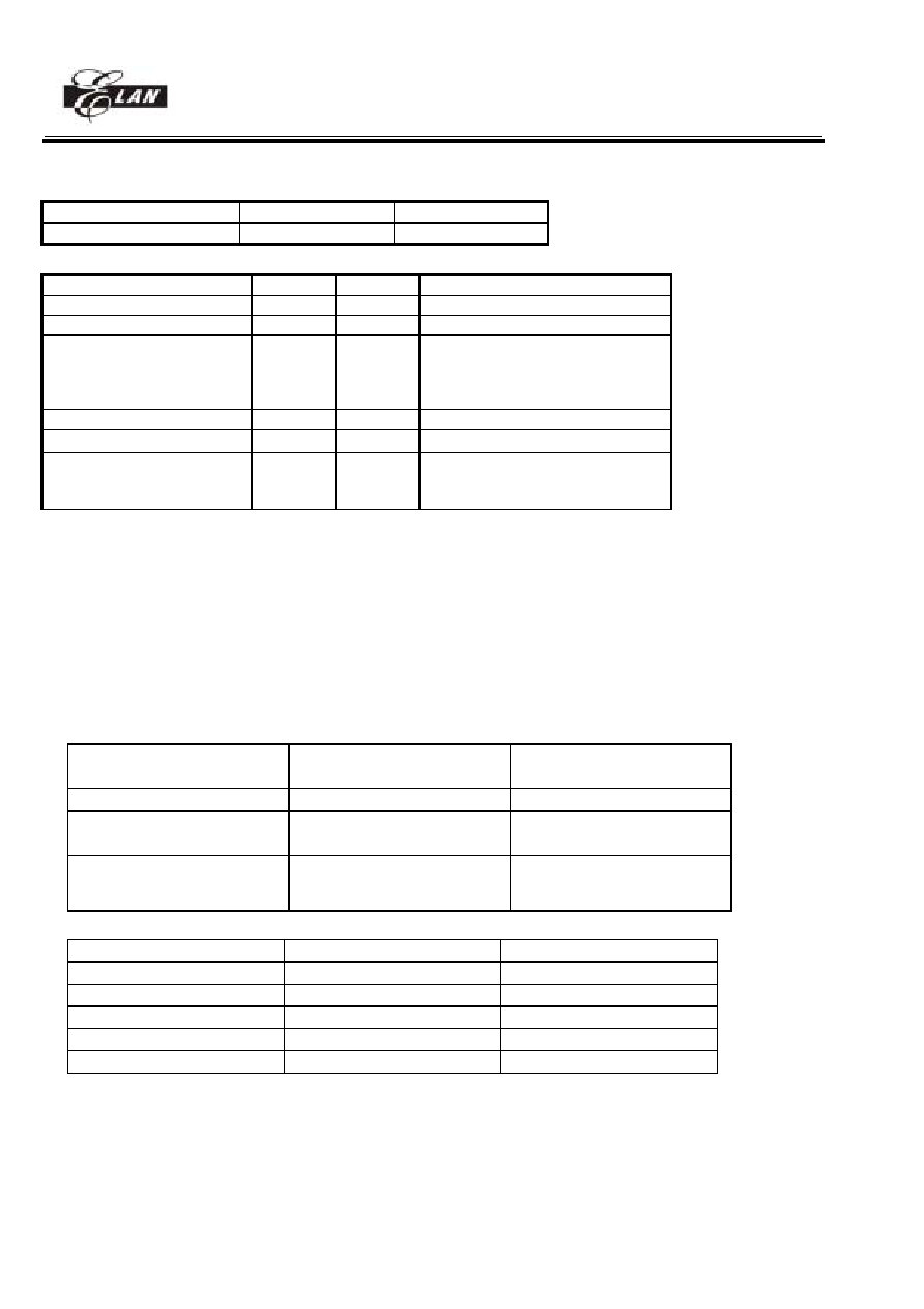
2. The difference between ICE 808 , EM78P808 and EM78871 are listed in the table
ICE 808
EM78P808
EM78871
Comparator reference voltage VDD
VDD or 2V
VDD or 2V
Stack pointer
O
O
X
Data Rom
O
O
X
(R6 page1 bit0-7&R7 page1
bit0- 7&R8 page1 bit0-7& R9 page1
bit0-1 unused)
RE page1 bit4
O
O
X(unused)
IOCE page1 bit0-1
O
O
X(unused)
RE page1 bit7-6
IOCE page2 bit0-2, bit4-6
code option bit0
O O X(unused)
3. "While switching main clock (regardless of high freq to low freq or on the other hand), adding 6
instructions delay (NOP) is required."
4. For DATA RAM least address(A0~A7), when using "INC" instruction and overflow occur,
the middle address will auto_increase. If using "DEC" instruction and least address from
0x00 0xFF, the middle address can't auto_decrease.
5. When Tip and Ring signals come, user cans choice one of FSK or DTMF receiver to decode.
The Operation Registers Setup as follows:
FSK
(RA PAGE0 bit 3)
DTMF
(IOC9 PAGE1 bit 7)
FSK or DTMF
0
0
All decoder off
0 1
DTMF
on
FSK off
1
X
(don't care)
FSK on
DTMF off
6.Die Pin difference
EM78P808
EM78871
Pin
136 pins
132 pins
EGIN1 V
X
EGIN2 V
X
Power PAD
2(VDD pin & AVDD pin) 1(VDD/AVDD pin)
Gnd PAD
2(AVSS pin & GND pin) 1(AVSS/GND
pin)
7.Don't switch to sleep mode from normal mode directly. Before do this, please
switch to green mode first.
8.Don't allow enable Idle Mode Function. (RA Page0 bit 7 don't allow set to 1)

EM78871
8-bit Micro-controller
__________________________________________________________________________________________________________________________________________________________________
* This specification is subject to be changed without notice.
8/23/04 (V1.5)
4
I.General Description
The EM78871 is an 8-bit CID (Call Identification) RISC type microprocessor with low power, high speed CMOS
technology. Integrated onto a single chip are on chip watchdog (WDT), RAM, program ROM, programmable real time
clock/counter, external/internal interrupt, power down mode, LCD driver, FSK decoder, Call waiting decoder, DTMF
receiver, Programming Tone generator, build-in KEY TONE clock generation, Comparator and tri-state I/O. The
EM78871 provides a single chip solution to design a CID of calling message display.
II.Feature
CPU
∑
Operating voltage range : 2.2V~5.5V(Normal mode), 2.0V~5.5V(Green mode)
∑
32K◊13 on chip Program ROM
∑
4K◊8 on chip data RAM
∑
144 byte working register
∑
Up to 51 bi-directional tri-state I/O ports (32 shared with LCD Segment pins)
∑
IO with internal Pull high, wake-up and interrupt functions
∑
STACK: 32 level stack for subroutine nesting
∑
TCC: 8-bit real time clock/counter (TCC) with 8-bit prescaler
∑
COUNTER1: 8-bit counter with 8-bit prescaler can be an interrupt source
∑
COUNTER2: 8-bit counter with 8-bit prescaler can be an interrupt source
∑
Watch Dog : Programmable free running on chip watchdog timer
∑
CPU modes:
Mode
CPU status
Main clock
32.768kHz clock status
Sleep mode
Turn off
Turn off
Turn off
Green mode
Turn on
Turn off
Turn on
Normal mode Turn on
Turn on
Turn on
∑
13 interrupt source , 8 external , 5 internal
∑
Key Scan : Port key scan function up to 16x4 keys
∑
Sub-Clock: 32.768KHz crystal
∑
Main-clock: 3.5862MHz multiplied by 0.25, 0.5, 1 or 3 generated by internal PLL
∑
Key tone output :4KHz, 2KHz ,1KHz (shared with IO)
∑
Comparator: 3-channel comparators: internal (16 level) or external reference voltage. (shared with IO)
∑
Serial Peripheral Interface (SPI): Interrupt flag available for the read buffer full, Programmable baud rates of
communication, Three-wire synchronous communication. (shared with IO)
Current D/A
∑
Operation Voltage : 2.5V5.5V
∑
7-bit resolution and 3-bit output level control
∑
Current DA output can drive speaker through a transistor for sound playing. (shared with IO)
Programmable Tone Generators
∑
Operation Voltage 2.2V5.5V
∑
Programmable Tone1 and Tone2 generators
∑
Independent single tone generation for Tone1 and Tone2
∑
Mixed dual tone generation by Tone1 and Tone2 with 2dB difference
∑
Can be programmed for DTMF tone generation
∑
Can be programmed for FSK signal (Bell202 or V.23) generation
CID
∑
Operation Voltage 2.7V5.5V for FSK
∑
Operation Voltage 2.7V5.5V for DTMF receiver
∑
Compatible with Bellcore GR-30-CORE (formerly as TR-NWT-000030)
∑
Compatible with British Telecom (BT) SIN227 & SIN242
∑
FSK demodulator for Bell 202 and ITU-T V.23 (formerly as CCITT V.23)
CALL WAITING
∑
Operation Voltage 2.6V5.5V

EM78871
8-bit Micro-controller
__________________________________________________________________________________________________________________________________________________________________
* This specification is subject to be changed without notice.
8/23/04 (V1.5)
5
∑
Compatible with Bellcore special report SR-TSV-002476
∑
Call-Waiting (2130Hz plus 2750Hz) Alert Signal Detector
∑
Good talkdown and talkoff performance
∑
Sensitivity compensated by adjusting input OP gain
LCD (8x80, 9x80, 16x80, 24x72)
∑
Maximum common driver pins : 16/24
∑
Maximum segment driver pins : 80(SEG0..SEG79)/72(SEG8..SEG79)
∑
Shared COM16 ~ COM23 pins with SEG0 ~ SEG7 pins
∑
1/4 bias for 8, 9 and 16 common mode and 1/5 bias for 24 common mode
∑
1/8, 1/9, 1/16, 1/24 duty
∑
16 Level LCD contrast control (software)
∑
Internal resistor circuit for LCD bias
∑
Internal voltage follower for better display
Die type
∑
132 pin die : EM78871H
∑
128 pin package : (EM78871AQ POVD disable, EM78871BQ POVD enable)
III.Application
1. adjunct units
2. answering machines
3. feature phones

