 | –≠–ª–µ–∫—Ç—Ä–æ–Ω–Ω—ã–π –∫–æ–º–ø–æ–Ω–µ–Ω—Ç: A6130DL8A | –°–∫–∞—á–∞—Ç—å:  PDF PDF  ZIP ZIP |
High Efficiency Linear Power Supply with Accurate
Power Surveillance and Software Monitoring
Features
Highly accurate 5 V, 100 mA guaranteed output
Low dropout voltage, typically 380 mV at 100 mA
Low quiescent current, typically 155 µA
Standby mode, maximum current 340 µA (with
100 µA load on OUTPUT)
Unregulated DC input can withstand -20 V reverse
battery and +60 V power transients
Fully operational for unregulated DC input voltage up
to 26 V and regulated output voltage down to 3.0 V
Reset output guaranteed for regulated output voltage
down to 1.2 V
No reverse output current
Very low temperature coefficient for the regulated
output
Current limiting
Comparator for voltage monitoring, voltage reference
1.17V
±2.2% voltage reference accuracy at +25∞C
±4.2% voltage reference accuracy from -40 to +85∞C
Programmable reset voltage monitoring
Programmable power on reset (POR) delay
Watchdog with programmable time windows
guarantees a minimum time and a maximum time
between software clearing of the watchdog
Time base accuracy ±10%
System enable output offers added security
TTL/CMOS compatible
-40 to +85∞C temperature range
DIP8 and SO8 packages
Description
The A6130 offers a high level of integration by combining
voltage regulation, voltage monitoring and software mon-
itoring in an 8 lead package. The voltage regulator has a
low dropout voltage (typ. 380 mV at 100 mA) and a low
quiescent current (155 µA). The quiescent current in-
creases only slightly in dropout prolonging battery life.
Built-in protection includes a positive transient absorber
for up to 60 V (load dump) and the ability to survive an un-
regulated input voltage of -20 V (reverse battery). The in-
put may be connected to ground or a reverse voltage
without reverse current flow from the output to the input. A
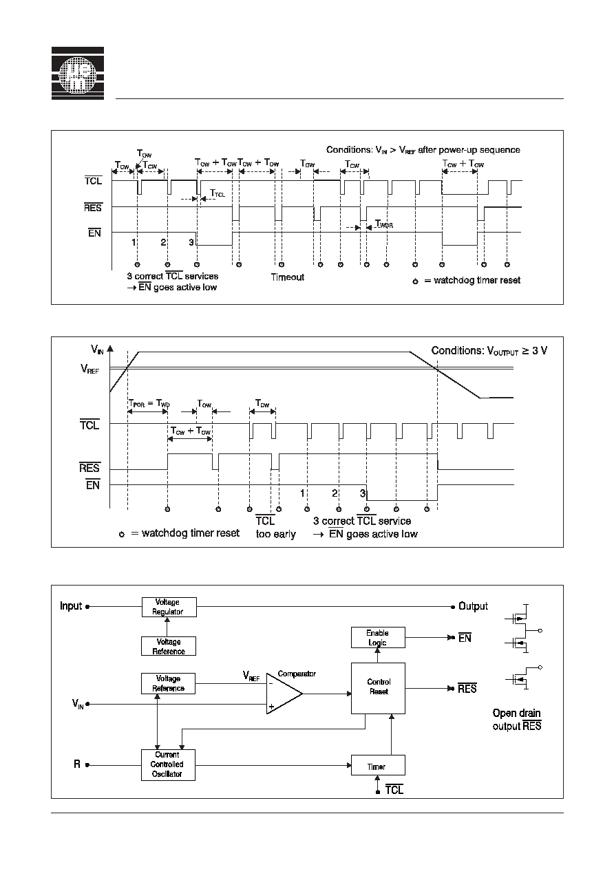
comparator monitors the voltage applied at the V
IN
input
comparing it with an internal 1.17 V reference. The
power-on reset function is initialized after V
IN
reaches 1.17
V and takes the reset output inactive after T
POR
depending
of external resistance. The reset output goes active low
when the V
IN
voltage is less than 1.17 V. The RES and EN
outputs are guaranteed to be in a correct state for a regu-
lated output voltage as low as 1.2 V. The watchdog func-
tion monitors software cycle time and execution. If soft-
ware clears the watchdog too quickly (incorrect cycle
time) or too slowly (incorrect execution) it will cause the
system to be reset. The system enable output prevents
critical control functions being activated until software
has successfully cleared the watchdog three times. Such
a security could be used to prevent motor controls being
energized on repeated resets of a faulty system.
Applications
Industrial electronics
Cellular telephones
Security systems
Battery powered products
High efficiency linear power supplies
Automotive electronics
1
A6130
EM MICROELECTRONIC-MARIN SA
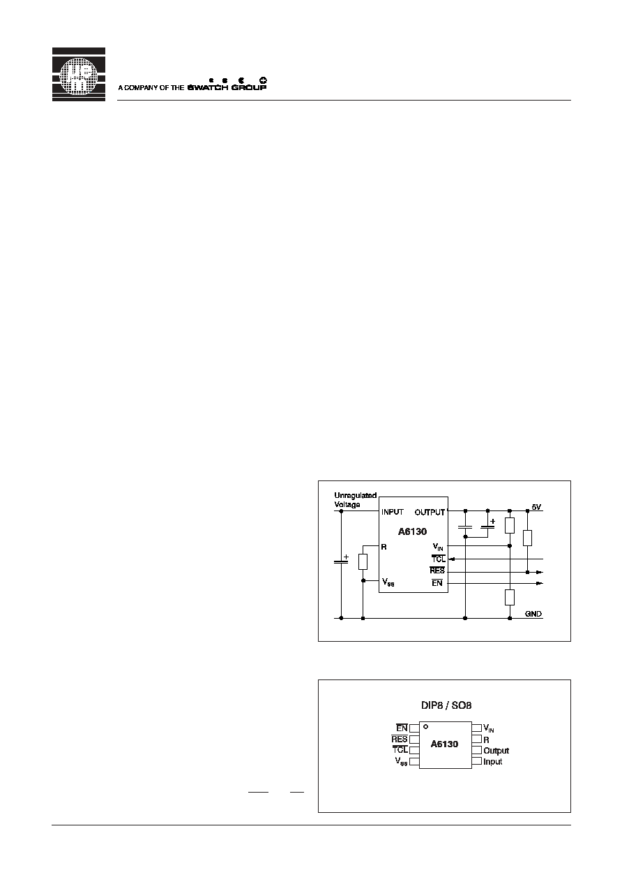
Typical Operating Configuration
Pin Assignment
Fig. 1
Fig. 2

Absolute Maximum Ratings
Parameter
Symbol Conditions
Continuous voltage at INPUT to
V
SS
V
INPUT
-0.3 to +30 V
Transients on INPUT for
t< 100 ms and duty cycle 1%
V
TRANS
up to +60 V
Reverse supply voltage on INPUT V
REV
-20 V
Max. voltage at any signal pin
V
MAX
OUTPUT+0.3V
Min. voltage at any signal pin
V
MIN
V
SS
-0.3V
Storage temperature
T
STO
-65 to +150∞C
Electrostatic discharge max. To
MIL-STD-883C method 3015
V
Smax
1000V
Max. soldering conditions
T
Smax
250∞C x 10 s
Table 1
Stresses above these listed maximum ratings may cause
permanent damage to the device. Exposure beyond
specified operating conditions may affect device reliabil-
ity or cause malfunction.
Handling Procedures
This device has built-in protection against high static volt-
ages or electric fields; however, anti-static precautions
must be taken as for any other CMOS component. Unless
otherwise specified, proper operation can only occur
when all terminal voltages are kept within the supply volt-
age range. At any time, all inputs must be tied to a de-
fined logic voltage level.
Operating Conditions
Parameter
Symbol Min. Max. Units
Operating junction
temperature
1)
T
J
-40
+85
∞C
INPUT voltage
2)
V
INPUT
2.3
26
V
OUTPUT voltage
2) 3)
V
OUTPUT
1.2
V
RES & EN guaranteed
4)
V
OUTPUT
1.2
V
OUTPUT current
5)
I
OUTPUT
100
mA
Comparator input voltage
V
IN
0
V
OUTPUT
V
RC-oscillator programming
R
10
1000
k
W
Thermal resistance from
junction to ambient
6)
- DIP8
R
th(j-a)
105
∞C/W
- SO8
R
th(j-a)
160
∞C/W
Table 2
1)
The maximum operating temperature is confirmed by
sampling at initial device qualification. In production, all
devices are tested at +85∞C.
2)
Full operation guaranteed. To achieve the load regulation
specified in Table 3 a 22 µF capacitor or greater is required
on the INPUT, see Fig. 8. The 22 µF must have an effective
resistance
£ 5 W and a resonant frequency above 500 kHz.
3)
A 10 µF load capacitor and a 100 nF decoupling capacitor
are required on the regulator OUTPUT for stability. The 10 µF
must have an effective series resistance of
£ 5 W and a
resonant frequency above 500 kHz.
4)
RES must be pulled up externally to V
OUTPUT
even if it is
unused. (Note: RES and EN are used as inputs by EM test.)
5)
The OUTPUT current will not apply for all possible
combinations of input voltage and output current.
Combinations that would require the A6130 to work above
the maximum junction temperature (+85∞C) must be
avoided.
6)
The thermal resistance specified assumes the package is
soldered to a PCB.
2
A6130
3
A6130
Electrical Characteristics
V
INPUT
= 6.0 V, C
L
= 10 µF + 100 nF, C
INPUT
= 22 µF, T
J
= -40 to +85∞C, unless otherwise specified
Parameter
Symbol
Test Conditions
Min.
Typ.
Max.
Unit
Supply current in standby mode
I
SS
R
EXT
= don't care, TCL = V
OUTPUT
,
V
IN
= 0 V, I
L
= 100 µA
340
µA
Supply current
1)
I
SS
R
EXT
= 100 k
W, I/Ps at V
OUTPUT
,
O/Ps 1 M
W to V
OUTPUT
, I
L
= 100 µA
155
400
µA
Supply current
1)
I
SS
R
EXT
= 100 k
W, I/Ps at V
OUTPUT
,
V
INPUT
= 8.0 V, O/Ps 1M
W to V
OUTPUT
,
I
L
= 100 mA
1.7
4.2
mA
Output voltage
V
OUTPUT
I
L
= 100 µA
4.88
5.12
V
Output voltage
V
OUTPUT
100 µA
£ I
L
£ 100 mA,
-40∞C
£ T
J
£ +85∞C
4.85
5.15
V
Output voltage temperature
coefficient
2)
V
th(coeff)
50
180
ppm/∞C
Line regulation
3)
V
LINE
6 V
£ V
INPUT
£ 26 V, I
L
= 1 mA,
T
J
= +85∞C
0.2
0.5
%
Load regulation
3)
V
L
100 µA
£ I
L
£ 100 mA
0.2
0.6
%
Dropout voltage
4)
V
DROPOUT
I
L
= 100 µA
40
170
mV
Dropout voltage
4)
V
DROPOUT
I
L
= 100 µA
380
mV
Dropout voltage
4)
V
DROPOUT
I
L
= 100 mA, -40∞C
£ T
J
£ +85∞C
650
mV
Dropout supply current
I
SS
V
INPUT
= 4.5 V, I
L
= 100 µA,
R
EXT
= 100 k
W, O/Ps 1 MW to
V
OUTPUT
, I/Ps at V
OUTPUT
1.2
1.6
mA
Thermal regulation
5)
V
thr
T
J
= +25∞C, I
L
= 50 mA,
V
INPUT
= 26 V, T = 10 ms
0.05
0.25
%/W
Current limit
I
Lmax
OUTPUT tied to V
SS
450
mA
OUTPUT noise, 10 Hz to 100kHz
V
NOISE
200
µV rms
3.0
£ V
OUTPUT
£ 5.5 V, I
L
= 100 µA. C
L
= 10 µF + 100 nF, C
INPUT
= 22 µF, T
J
= -40 to +85∞C, unless otherwise specified
RES and EN
Output Low Voltage
V
OL
V
OUTPUT
= 4.5 V, I
OL
= 20 mA
0.4
V
V
OL
V
OUTPUT
= 4.5 V, I
OL
= 8 mA
0.2
0.4
V
V
OL
V
OUTPUT
= 2.0 V, I
OL
= 4 mA
0.2
0.4
V
V
OL
V
OUTPUT
= 1.2 V, I
OL
= 0.5 mA
0.06
0.2
V
EN
Output High Voltage
V
OH
V
OUTPUT
= 4.5 V, I
OH
= -1 mA
3.5
4.1
V
V
OH
V
OUTPUT
= 2.0 V, I
OH
= -100 µA
1.8
1.9
V
V
OH
V
OUTPUT
= 1.2 V, I
OH
= -30 µA
1.0
1.1
V
TCL and V
IN
TCL Input Low Level
V
IL
V
SS
0.8
V
TCL Input High Level
V
IH
2.0
V
OUTPUT
V
Leakage current TCL input
I
LI
V
SS
£ V
TCL
£ V
OUTPUT
0.05
1
µA
V
IN
input resistance
R
VIN
100
M
W
Comparator reference
6)7)
V
REF
T
J
= +25∞C
1.148
1.170
1.200
V
V
REF
20∞C
£ T
J
£ +70∞C
1.123
1.218
V
V
REF
1.123
1.222
V
Comparator hysteresis
7)
V
HY
2
mV
Table 3
1)
If INPUT is connected to V
SS
, no reverse current will flow from the OUTPUT to the INPUT, however the supply current specified
will be sank by the OUTPUT to supply the A6130.
2)
The OUTPUT voltage temperature coefficient is defined as the worst case voltage change divided by the total temperature range.
3)
Regulation is measured at constant junction temperature using pulse testing with a low duty cycle. Changes in OUTPUT voltage
due to heating effects are covered in the specification for thermal regulation.
4 )
The dropout voltage is defined as the INPUT to OUTPUT differential, measured with the input voltage equal to 5.0 V.
5 )
Thermal regulation is defined as the change in OUTPUT voltage at a time T after a change in power dissipation is applied,
excluding load or line regulation effects.
6)
The comparator and the voltage regulator have separate voltage references (see Block Diagram Fig. 7).
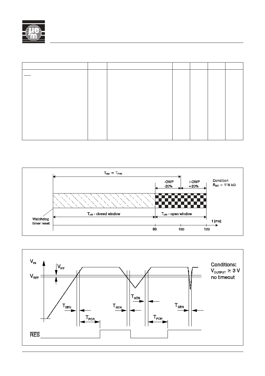
7)
The comparator reference is the power-down reset threshold. The power-on reset threshold equals the comparator reference
voltage plus the comparator hysteresis (see Fig. 4).
4
A6130
Timing Characteristics
V
INPUT
= 6.0 V, I
L
= 100 µA, C
L
= 10 µF + 100 nF, C
INPUT
= 22 µF, T
J
= -40 to +85∞C, unless otherwise specified
Parameter
Symbol Test Conditions
Min.
Typ.
Max.
Units
Propagation delays:
TCL to Output Pins
T
DIDO
250
500
ns
V
IN
sensitivity
T
SEN
1
5
20
µs
Logic Transition Times on all
Output Pins
T
TR
Load 10 k
W, 50 pF
30
100
ns
Power-on Reset delay
T
POR
R
EXT
= 118 k
W, ± 1%
90
100
110
ms
Watchdog Time
T
WD
R
EXT
= 118 k
W, ± 1%
90
100
110
ms
Open Window Percentage
OWP
±0.2 T
WD
Closed Window Time
T
CW
0.8 T
WD
T
CW
R
EXT
= 118 k
W, ± 1%
72
80
88
ms
Open Window Time
T
OW
0.4 T
WD
T
OW
R
EXT
= 118 k
W, ± 1%
36
40
44
ms
Watchdog Reset Pulse
T
WDR
T
WD
/ 40
T
WDR
R
EXT
= 118 k
W, ± 1%
2.5
ms
T
CL
Input Pulse Width
T
TCL
150
ns
Table 4
Timing Waveforms
Watchdog Timeout Period
Voltage Monitoring
Fig. 3
Fig. 4
5
A6130
Timer Reaction
Combined Voltage and Timer Reaction
Block Diagram
Fig. 5
Fig. 6
Fig. 7