Äîêóìåíòàöèÿ è îïèñàíèÿ www.docs.chipfind.ru
EM4005
EM4105
Copyright
©
200, EM Microelectronic-Marin SA
1
www.emmicroelectronic.com
ISO 11'784 / 11'785 Compliant Read Only Contactless Identification Device
Description
The EM4005/EM4105 (previously named H4005/H4105)
is a CMOS integrated circuit intended for use in electronic
Read Only RF Transponders. The circuit is powered by an
external coil placed in an electromagnetic field, and gets
its master clock from the same field via one of the coil
terminals. The other coil terminal is affected by the
modulator. By turning on and off the modulation current,
the chip will send back the 128 bits of information
contained in a factory pre-programmed memory array.
The programming of the chip is performed by laser fusing
of polysilicon links in order to store a unique code on each
chip.
Due to the low power consumption of the logic core, no
supply buffer capacitor is required. Only an external coil is
needed to obtain the chip function. A parallel resonance
capacitor of 75 pF is also integrated.
Features
128 bit memory array laser programmable
Bit duration : 32 periods of RF field
Bit coding according to ISO FDX-B
On chip resonance capacitor
On chip supply buffer capacitor
Wide
dynamic
range
On chip voltage limiter
Full
wave
rectifier
Large modulation depth
Operating frequency 100 - 150 kHz
Very small chip size convenient for implantation
Very low power consumption
Applications
Animal implantable transponder
Animal
ear
tag
Industrial
transponder
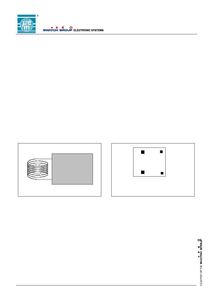
Typical Operating Configuration
Coil1
Coil2
EM4005
Fig.
1
Pin Assignment
COIL 1 Coil terminal / Clock input
COIL 2 Coil terminal
EM4005
COIL2
COIL1
VDD
VSS
Fig.
2
EM MICROELECTRONIC -
MARIN SA
EM4005
EM4105
Copyright
©
200, EM Microelectronic-Marin SA
2
www.emmicroelectronic.com
Absolute Maximum Ratings
Parameter Symbol
Conditions
Maximum AC peak Current
induced on COIL1 and COIL2
Power Supply
Storage temperature Die form
Storage temperature PCB
form
Electrostatic discharge
maximum to MIL-STD-883C
method 3015
ICOIL
V
DD
Tstore
Tstore
VESD
± 30 mA
-0.3 to 7.5 V
-55 to +200°C
-55 to +125°C
1000 V
Stresses above these listed maximum ratings may cause
permanent damages to the device. Exposure beyond
specified operating conditions may affect device reliability
or cause malfunction.
Handling Procedures
This device has built-in protection against high static
voltages or electric fields; however, anti-static precautions
must be taken as for any other CMOS component. Unless
otherwise specified, proper operation can only occur when
all terminal voltages are kept within the voltage range.
Unused inputs must always be tied to a defined logic
voltage level.
Operating Conditions
Parameter Symb
Min
Typ
Max
Unit
Operating Temp.
Maximum coil current
AC Voltage on Coil
Supply Frequency
Top
ICOIL
Vcoil
fcoil
-40
100
14*
+85
10
150
°C
mA
Vpp
kHz
*) The AC Voltage on Coil is limited by the on chip voltage
limitation circuitry.
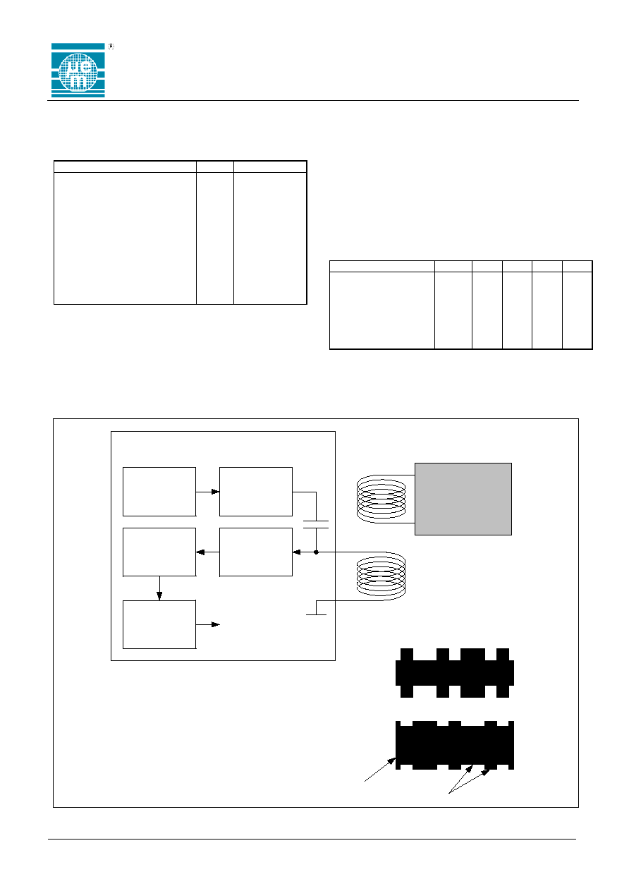
System Principle
Antenna
Driver
Oscillator
Demodulator
Filter
and
Gain
Data decoder
Data received
from transponder
Tranceiver
Transponder
Coil1
Coil2
EM4005
Signal on coils
Transponder coil
Transeiver coil
RF Carrier
Data
Fig. 3
EM4005
EM4105
Copyright
©
200, EM Microelectronic-Marin SA
3
www.emmicroelectronic.com
Electrical Characteristics
V
DD
= 1.5 V V
SS
= 0 V fcoil = 134 kHz Square wave Top = 25°C
V
C1
= 1.0 V with positive peak at V
DD
and negative peak at V
DD
- 1 V unless otherwise specified
Parameter Symbol
Test
conditions Min
Typ
Max
Units
Supply Voltage
Supply Current
Rectified Supply Voltage
C2 pad Modulator ON
voltage drop
C1 pad Modulator ON
voltage drop
Coil1 - Coil2 capacitance
Power Supply Capacitor
V
DD
I
DD
V
DD
V
ONC2
V
ONC1
C
res
C
sup
VC2 -VC1 = 2.8 VDC
Modulator Switch = "ON"
VDD = 1.5V IVDDC2 = 100 µA
with ref. to VDD
VDD = 5.0V IVDDC2 = 1 mA with
ref. to VDD
VDD = 5.0V IVDDC1 = 1 mA with
ref. to VDD
Vcoil = 100 mVRMS f = 10 kHz
1.5
1.5
0.9
2.1
2.1
75
2)
150
1)
1.5
1.3
3.0
3.0
V
µA
V
V
V
V
pF
pF
Note 1) The maximum voltage is defined by forcing 10 mA on C1 - C2
Note 2) The tolerance of the resonant capacitor is ± 15 % over the whole production. On a wafer basis and on process
statistics, the tolerance is ± 2%
Timing Characteristics
V
DD
= 1.5 V V
SS
= 0 V fcoil = 134 kHz Sine wave Top = 25°C
V
C1
= 1.0 V with positive peak at V
DD
and negative peak at V
DD
- 1 V unless otherwise specified
Timings are derived from the field frequency and are specified as a number of RF periods.
Parameters Symbol
Test
Conditions Value
Units
Read bit period
trdb
32
RF periods
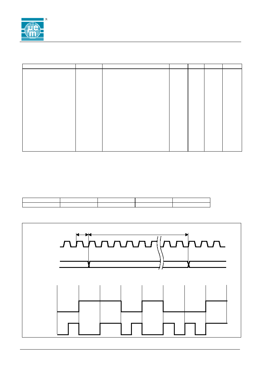
Timing Waveforms
Serial Data Out
COIL1
OC
T
BIT n
32 OC
T
BIT n+1
BIT n+2
Binary Data
Memory Output
Modulator Output
0
1
1
0
1
0
0
1
Fig. 4
EM4005
EM4105
Copyright
©
200, EM Microelectronic-Marin SA
4
www.emmicroelectronic.com
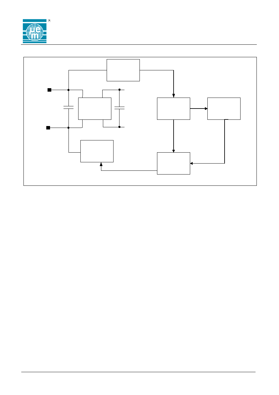
Block Diagram
CLOCK
EXTRACTOR
FULL WAVE
RECTIFIER
DATA
MODULATOR
SEQUENCER
DATA
ENCODER
MEMORY
ARRAY
Logic
Clock
Serial
Data Out
Modulation
Control
Cress
COIL1
COIL2
AC1
AC2
+
-
Csup
VDD
VSS
Fig. 5
Functional Description
General
The EM4005 is supplied by means of an electromagnetic
field induced on the attached coil. The AC voltage is
rectified in order to provide a DC internal supply voltage.
When the DC voltage is sufficient the chip sends data
continuously. When the last bit is sent, the chip will
continue with the first bit until the power goes off.
Full Wave Rectifier
The AC input induced in the external coil by an incident
magnetic field is rectified by a Graetz bridge. The bridge
will limit the internal DC voltage to avoid malfunction in
strong fields.
Clock extractor
One of the coil terminals (COIL1) is used to generate the
master clock for the logic function. The output of the clock
extractor drives a sequencer.
Sequencer
The sequencer provides all necessary signals to address
the memory array and to encode the serial data out. The
data rate is set to 32 clocks per bit.
Data Encoder
The data is coded according to the FDX-B scheme. At the
beginning of each bit, a transition will occur. A logic bit "1"
will keep its state for the whole bit duration and a logic bit
"0" will show a transition in the middle of the bit duration
(refer to fig. 4).
The FDX-B allows an advance of up to 8 clocks in the ON
to OFF transition. Due to its low power consumption, there
is no difference in performance for the H4005 when
implementing a transition advance. No clock advance is
provided on the standard version.
Data Modulator
The data modulator is controlled by the signal Modulation
Control in order to induce a high current on COIL2
terminal when this signal is at logic "0". This will affect the
magnetic field according to the data stored in the memory
array.
Memory
The memory contains 128 bits laser programmed during
manufacturing according to a customer list of codes. The
bits are read serially in order to control the modulator. The
128 bits output sequence is repeated continuously until
power goes off.
EM4005
EM4105
Copyright
©
200, EM Microelectronic-Marin SA
5
www.emmicroelectronic.com
Memory Map
Header
11 bits
Identification code
64 bits + 8 trail bits
CRC
16 bits + 2 trail bits
Extension
24 bits + 3 trail bits
1..............11 12.....................................83 84............................101 102........................128
Bit 1 send first
National code
38 bits + 4 trail bits
Country
10 bits + 1 trail bit
Data
B
l
ock
An
im
al
Reserved code
14 bits + 3 trail bits
LSBs of each registers are sent first
64 bit pattern identification ISO 11'784
128 bit pattern identification ISO 11'785
Fig. 6
Memory organisation
The structure of the 128 bits is as follows :
The header is sent first and is used to identify the start of
the sequence. It is composed of 11 bits having a bit
pattern which is unique in the data stream.
00000000001
The header is followed by the Identification code which
is composed of 64 bits organised in 8 blocks of 8 bits.
Each block of 8 bits is trailed by a control bit set to logic
"1" to prevent that the header is reproduced in the data.
Bit 64 is transmitted first.
Bit 1 is a flag for animal "1" or non-animal "0" application.
Bits 2-15 are a reserved code for future use.
Bit 16 is a flag for additional data block "1" or no additional
data block "0".
Bits 17-26 ISO 3166 Numeric country code
Bits 27-64 National identification code
The next two 8 bit blocks contain the 16 CRC-CCITT error
detection bits. LSB is transmitted first, and the 2 block are
trailed with a binary "1".
The data stream with 3 blocks of 8 bits trailed with a
logical "1" representing the extension bits. The extension
bits are planned for future extension in which for instance
information from sensors or contents of trailing pages may
be stored. In the current version the standard coding will
be 000000001 000000001 000000001 and the flag bit 16
of the identification code "0".
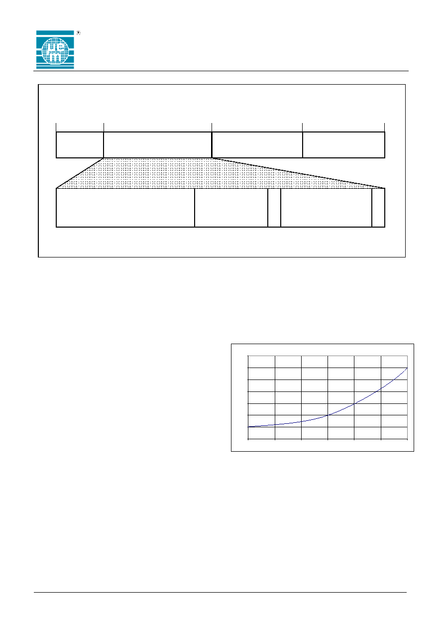
Resonance Capacitor
The Resonance Capacitor is integrated, and its value is
typically 75 pF.
Resonnance capacitor versus temperature
99.6
99.8
100
100.2
100.4
100.6
100.8
101
-50
-25
0
25
50
75
100
Top [°C]
Resonnance capacitor [%]
Fig. 7