
EM4095
Copyright
2002, EM Microelectronic-Marin SA
1
www.emmicroelectronic.com
Read/Write analog front end for 125kHz RFID Basestation
Description
The EM4095 (previously named P4095) chip is a CMOS
integrated transceiver circuit intended for use in an RFID
basestation to perform the following functions:
- antenna driving with carrier frequency
- AM modulation of the field for writable transponder
- AM demodulation of the antenna signal modulation
induced by the transponder
communicate with a microprocessor via simple interface.
Features
Integrated PLL system to achieve self adaptive
carrier frequency to antenna resonant frequency
No external quartz required
100 to 150 kHz carrier frequency range
Direct antenna driving using bridge drivers
Data transmission by OOK (100% Amplitude
Modulation) using bridge driver
Data transmission by Amplitude Modulation with
externally adjustable modulation index using single
ended driver
Multiple transponder protocol compatibility
(Ex: EM400X, EM4050, EM4150, EM4070, EM4170,
EM4069....)
Sleep
mode
1µA
USB compatible power supply range
40 to +85∞C temperature range
Small outline plastic package SO16
Applications
Car immobiliser
Hand held reader
Low cost reader
Typical Operating Configuration
Read Only Mode
µP
+5V
L
A
C
DV1
C
DV2
C
RES
P4095
2
3
4
5
6
7
8
1
15
14
13
12
11
10
9
16
+5V
RDY/CLK
C
DEC
C
AGND
MOD
DEMOD_OUT
SHD
C
DC2
C
FCAP
Fig. 1
Read/Write Mode
µP
+5V
L
A
C
DV1
C
DV2
C
RES
C
DEC
C
AGND
P4095
2
3
4
5
6
7
8
1
15
14
13
12
11
10
9
16
+5V
MOD
DEMOD_OUT
SHD
C
DC2
C
FCAP
RDY/CLK
Fig. 2
Pin Assignment
SO16
VSS
RDY/CLK
ANT1
DVDD
DVSS
ANT2
DC2
FCAP
SHD
DEMOD_OUT
MOD
AGND
VDD
CDEC_IN
DEMOD_IN
CDEC_OUT
Fig. 3
EM MICROELECTRONIC
- MARIN SA
EM4095
EM4095

EM4095
Copyright
2002, EM Microelectronic-Marin SA
2
www.emmicroelectronic.com
System principle
Signal on
Transponder coil
Signal on
Transceiver coil
Data
RF Carrier
DOWNLINK
Signal on
Transponder coil
Signal on
Transceiver coil
Data
RF Carrier
UPLINK
Transponder
Coil1
Coil2
Read Only
and
R/W Chip
µP
+5V
L
A
C
DV1
C
DV2
C
RES
EM4095
2
3
4
5
6
7
8
1
15
14
13
12
11
10
9
16
+5V
RDY/CLK
C
DEC
C
AGND
MOD
DEMOD_OUT
SHD
C
DC2
C
FCAP
Transceiver
R/W configuration
Fig. 4

EM4095
Copyright
2002, EM Microelectronic-Marin SA
3
www.emmicroelectronic.com
Absolute Maximum Ratings
Parameter
Symbol
Conditions
Storage temperature
T
STO
-55 to +150∞C
Maximum voltage at V
DD
V
DDmax
V
SS
+6V
Minimum voltage at V
DD
V
DDmin
V
SS
-0.3V
Max. voltage other pads
V
MAX
V
DD
+0.3V
Min. voltage other pads
V
MIN
V
SS
-0.3V
Max. junction temperature
T
JMAX
+125∞C
Electrostatic discharge max.
to MIL-STD-883C method
3015 against V
SS
V
ESD
4000V
Electrostatic discharge max.
to MIL-STD-883C method
3015 (only for pins ANT1
and ANT2) against V
SS
V
ESD_ANT
10000V
Maximum Input/Output
current on all pads except
VDD, VSS, DVDD, DVSS,
ANT1, ANT2, RDY/CLK
I
IMAX
I
OMAX
10mA
Maximum AC peak current
on ANT1 and ANT2 pads
100 kHz duty cycle 50%
I
ANTmax
300mA
Stresses above these listed maximum ratings may cause
permanent damages to the device. Exposure beyond
specified operating conditions may affect device reliability
or cause malfunction.
Handling Procedures
This device has built-in protection against high static
voltages or electric fields; however, anti-static precautions
must be taken as for any other CMOS component. Unless
otherwise specified, proper operation can only occur when
all terminal voltages are kept within the voltage range.
Unused inputs must always be tied to a defined logic
voltage level.
Operating Conditions
Parameter
Symb Min
Typ
Max
Units
Operating junction
temperature
T
J
-40
+110
∞C
Supply voltage
V
DD
4.1
5
5.5
V
Antenna circuit
resonant frequency
F
RES
100
125
150
kHz
AC peak current on
ANT1 & ANT2 pads
I
ANT
250
mA
C
FCAP
*
10
*
nF
C
DEC
*
100
*
nF
C
DC2
*
6.80
*
nF
C
AGND
100
220
nF
Package thermal
resistor SO16
R
th j-a
69
70
71
∞C/W
*
±10% tolerance capacitors should be used
** According to 1S2P JEDEC test board
Due to antenna driver current the internal junction temperature is
higher than ambient temperature. Please calculate ambient
temperature range from max. antenna current and package
Thermal Resistor. It is the user's responsibility to guarantee that
T
J
remains below 110∞C.
Supply voltage (V
DD
and DV
DD
pads) must be blocked by a 100nF
capacitor (to V
SS
) as close as possible to the chip
EM4095
Copyright
2002, EM Microelectronic-Marin SA
4
www.emmicroelectronic.com
Electrical and Switching Characteristics:
Parameters specified below are valid only in case the device is used according to Operating Conditions defined on previous
page.
V
SS
=D
VSS
=0V, V
DD
=D
VDD
= 5V, T
j
= -40 to 110∞C, unless otherwise specified
Parameter
Symbol
Test Conditions
Min
Typ
Max
Units
Supply current in sleep mode
I
DDsleep
1
2
µA
Supply current excluding drivers
current
I
DDon
5
7
mA
AGND level
V
AGND
Note 1
2.35
2.5
2.65
V
Logic signals SHD, MOD,
DEMOD_OUT
Input logic high
V
IH
0.8V
DD
V
Input logic low
V
IL
0.2V
DD
V
Output logic high
V
OH
I
SOURCE
=1mA
0.9V
DD
V
Output logic low
V
OL
I
SINK
=1mA
0.1V
DD
V
MOD pull down resistor
R
PD
0.2V
DD
20
50
90
k
SHD pull up resistor
R
PU
0.8V
DD
20
50
90
k
PLL
Antenna capture frequency range
F
ANT_C
100
150
kHz
Antenna locking frequency range
F
ANT_L
100
150
kHz
Drivers
ANT drivers output resistance
R
AD
I
ANT
=100mA
3
9
RDY/CLK driver output resistance
R
CL
I
RDY/CLK
=10mA
12
36
AM demodulation
DEMOD_IN common mode range
V
CM
V
SS
+ 0.5
V
DD
- 0.5
V
DEMOD_IN input sensitivity
V
sense
Note 2
0.85
2
mVpp
Note 1: A
GND
is a EM4095 internal reference point. Any external connection except specified capacitor to V
SS
may lead to
device malfunction.
Note 2: Modulating signal 2Khz square wave on 125 kHz carrier, total signal inside V
CM
Vsense
EM4095
Copyright
2002, EM Microelectronic-Marin SA
5
www.emmicroelectronic.com
Timing Characteristics:
Parameters specified below are valid only in case the device is used according to Operating Conditions defined on previous
page.
V
SS
=D
VSS
=0V, V
DD
=D
VDD
= 5V
Parameter
Symbol
Test Conditions
Typ
Max
Units
Set-up time after a sleep period
Tset
25
35
ms
Time from full power to modulation
state
Tmdon
antenna circuit specifications:
Q=15,FRES=125Khz
modulation index: 100%
50
µs
AM demodulation: Delay time from
input to output
Tpd
Modulating signal 2Khz square
wave 10mVpp
40
100
µs
Recovery time of reception after
antenna modulation
Trec
Note 1
400
500
µs
Note 1: RF period is time of one period transmitted on ANT outputs (at 125 kHz 8µs). Trec after antenna modulation
receiver chain is ready to demodulate. The condition is of course that the amplitude on antenna has already reached its
steady state by that time (this depends on Q of antenna). See also Application Notes.
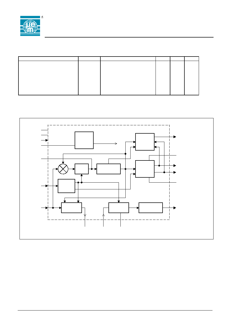
Block Diagram
VDD
SHD
AGND
VSS
to all blocks
LOOP
FILTER
VCO &
SEQUENCER
BIAS &
AGND
SHORT
DETECTION
& READY
BIAS & AGND
to all blocks
ANTENNA
DRIVERS
SYNCHRO
SAMPLER
FILTER
COMPARATOR
to all blocks
to all blocks
CDEC_OUT
CDEC_IN DC2
FCAP
MOD
DMOD_IN
RDY/CLK
DVDD
ANT1
ANT2
DVSS
DMOD_OUT
HOLD
LOCK
Fig. 5