Äîêóìåíòàöèÿ è îïèñàíèÿ www.docs.chipfind.ru
EM4170
Copyright
2002, EM Microelectronic-Marin SA
1
www.emmicroelectronic.com
125kHz CRYPTO READ/WRITE Contactless Identification Device
Description
The EM4170 is a CMOS integrated circuit intended for
use in electronic Read/Write RF Transponders. The chip
contains an implementation of a crypto-algorithm with 96
Bits of user configurable secret-key contained in
EEPROM. It also provides a unique Device Identification
of 32 bits that can never be modified as well as 94 bits of
freely programmable USER-MEMORY. Bits 15 and 14
of word 1 are used as Lock-Bits. The memory can only
be accessed for writing or erasing if these two bits have
the contents "x0" as when they are delivered.
The memory can be unlocked by using the PIN-code
command. In that case, the lock-bits are reset from the
value "x1" to the value "x0".
The EM4170 transmits data to the transceiver by
modulating the amplitude of the electromagnetic field,
and receives data and commands in a similar way.
The coil of the tuned circuit is the only external
component required, all remaining functions are
integrated in the chip.
Features
·
On Chip Crypto-Algorithm
·
Two Way Authentication
·
96 bits of Secret-Key in EEPROM (unreadable)
·
32 bits of fix Device Identification
·
32 bits of PIN code (unreadable)
·
94 bits of USER_MEMORY (UM) with read access
(OTP)
·
Secret-Key programmable via CID-Interface
·
Lock-Bits to inhibit programming
·
Data Transmission performed by Amplitude
Modulation
·
Bit Period = 32 periods of carrier frequency
·
200pF on chip Resonant Capacitor (untrimmed)
·
-40 to +85°C Temperature range
·
100 kHz to 150 kHz Field Frequency
·
On chip Rectifier and Voltage Limiter
·
No external supply buffer capacitance needed due
to low power consumption
Typical Applications
·
Anti-counterfeiting
·
High security hands-free access control
Typical Operating Configuration
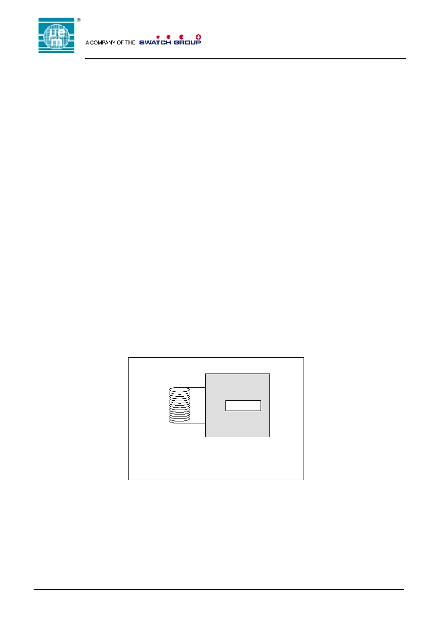
Fig. 1
COIL1
EM4170
L
Typical value for inductance L is 8mH at f
O
= 125 KHz
COIL2
EM MICROELECTRONIC
- MARIN SA
EM4170
Copyright
2002, EM Microelectronic-Marin SA
2
www.emmicroelectronic.com
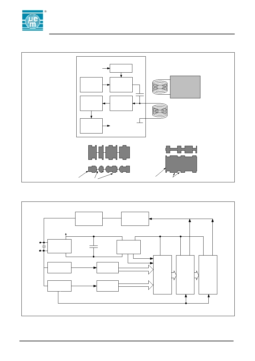
System Principle
READ MODE
Signal on
Transponder coil
Signal on
Transceiver coil
Data
RF Carrier
RECEIVE MODE
Antenna
Driver
Oscillator
Demodulator
Filter
and
Gain
Data decoder
Data received
from transponder
Tranceiver
Transponder
Coil1
Coil2
EM4170
Modulator
Data to be sent
to transponder
Signal on
Transponder coil
Signal on
Transceiver coil
Data
RF Carrier
Fig. 2
Block Diagram
Modulator
Encoder
AC/DC
converter
Clock
Extractor
Data
Extractor
Sequencer
Command
Decoder
Cr
V
POS_REG
RESET
PWR
Cs
GND
Control
Logic
EEPROM
Crypto-
Algorithm
V
DD
Serial
Data
Power
Control
Coil1
Coil2
Fig. 3
EM4170
Copyright
2002, EM Microelectronic-Marin SA
3
www.emmicroelectronic.com
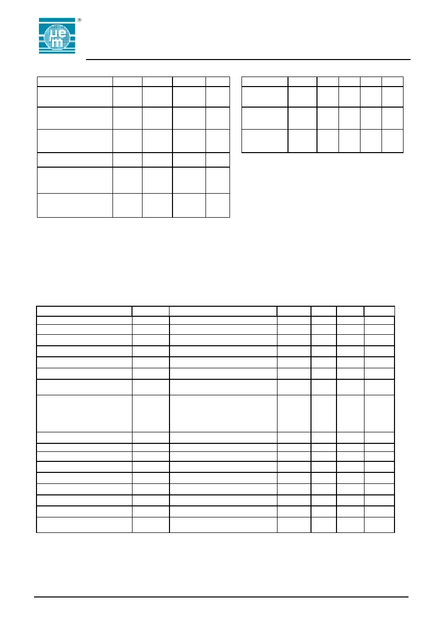
Absolute Maximun Ratings
Operating Conditions
Parameter
Symbol
Min.
Max.
Units
Parameter
Symbol Min.
Typ. Max. Units
Supply Voltage
(Unregulated)
V
POS-REG
-0.3
9.5
V
Operating
Temperature
T
OP
-40
+25
+85
°C
Supply Voltage
(regulated)
V
DD
-0.3
5.5
V
Maximum coil
current
I
COIL
-10
+10
mA
Voltage at remaining
pins Excepted COIL1,
COIL2
V
PIN
V
SS
- 0.3 V
DD
+ 0.3
V
Frequency on
Coil inputs
F
COIL
100
125
150
kHz
Storage temperature
T
store
-55
+ 125
°C
Electrostatic discharge
(Mil-STD-883 C method
3015)
V
ESD
1000
V
Maximum Current
induced on COIL1 and
COIL2
I
COIL
-30
+ 30
mA
Handling Procedure
Stresses above these listed maximum ratings may cause
permanent damage to the device. Exposure beyond specified
electrical characteristics may affect device reliability
Electrical parameters and functionality are not guaranteed
when the circuit is exposed to light.
This device has built-in protection against high static
voltages or electric fields; however, anti-static
precautions should be taken as for any other CMOS
component. Unless otherwise specified, proper
operation can only occur when all terminal voltages are
kept within the supply voltage range.
Electrical Characteristics
V
DD
= V
POS
_
REG
= 2.5V, V
SS
= 0V, f
coil
= 125 kHz Sine wave, V
coil
= 1V
pp,
T
op
= 25°C unless otherwise specified.
Parameter
Symbol
Conditions
Min.
Typ.
Max.
Units
Supply Voltage(unregulated)
V
POS-REG
V
POS_REG
= max (note 1)
1)
V
Supply Voltage (regulated)
V
DD
Read Mode (note 2)
2.8
3.5
4.2
V
EEPROM read voltage
V
RD
2.0
V
EEPROM write voltage
V
EE
2.5
V
Supply current / read
I
rd
Read Mode V
DD
=2.0V
5.0
µA
Supply current /write @25°C
I
wr25
Write Mode, V
DD
=2.5V
30
38
µA
Supply current / write
I
wr
Write Mode, V
DD
=2.6V
-40°C<T<85°C
70
µA
Modulator voltage drop
V
ON
V
Coil1
- V
SS
and V
Coil2
- V
SS
I
coil
= 100µA
V
Coil1
- V
SS
and V
Coil2
- V
SS
I
coil
= 5mA
0.30
0.45
0.60
2.50
V
V
Resonnance Capacitor
C
r
10 kHz, 100 mV
pp
170
200
230
pF
Capacitor temp. coeff
TKC
r
-40°C to 85°C
-75
+75
ppm/K
Capacitor tolerance/wafer
TOLC
r
-2
+2
%
POR level high
V
prh
Rising Supply
2.0
2.4
V
POR level low
V
prl
Falling Supply
1.8
2.2
V
Clock extractor input min
V
clkmin
Min for clock extraction
0.6
0.36
V
pp
Clock extractor input max
V
clkmax
Max for clock extraction
50
mV
pp
EEPROM data endurance
N
cy
Erase all / Write all
100000
cycles
EEPROM retention
T
ret
Top = 55°C after 100'000 cycles
(note 3)
10
years
Note 1 : Maximum voltage is defined by forcing 10mA on Coil1-Coil2
Note 2 : The circuit is not functional below the POR-level
Note 3 : Based on 1000 hours at 150°C

EM4170
Copyright
2002, EM Microelectronic-Marin SA
4
www.emmicroelectronic.com
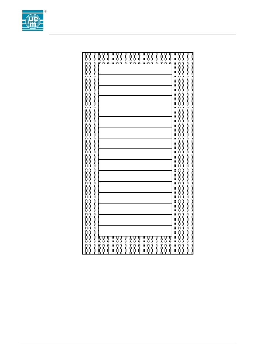
Timing Characteristics
Parameter
Symbol
Conditions
Min.
Typ.
Max.
Unit
Power on Reset Time
Read Bit Period
LIW/ACK/NACK pattern
Duration
Duration of ID
Divergency-Time
Authentication-Time
WRITE Access Time
EEPROM write time
WRITE Access Time of
the Lock Bits
t
por
t
rdb
t
patt
t
rID
T
div
t
auth
t
wa
t
wee
t
walb
V
DD
=3V
32
160
1536
224
4224
128
3072
672
600
µs
periods
periods
periods
periods
periods
periods
periods
periods
RF periods represent periods of the carrier frequency emitted by the transceiver unit. For example, if 125kHz is used,
the Read bit period would be: 1/125'000*32 = 256µs.
Functional Description
The EM4170 is supplied by means of an electromagnetic
field induced on the attached coil. The AC voltage is
rectified in order to provide a DC internal supply voltage.
When the DC voltage crosses the Power-On level, the
chip will enter the Standby Mode and expect commands.
In Standby Mode a continuous sequence of Listen
Windows (LIW) is generated. During this time, the
crypto-Chip will turn to the Receive Mode (RM) if it
receives a valid RM pattern. The chip then expects a
command to enter the desired mode of operation.
Memory Organisation
The 256 bits EEPROM are organised in 16 words of 16
bits. Words 0 and 1 contain the USER_MEMORY_1 and
the Lock-Bits LB1 and LB0. Words 12, 13, 14 and 15
contain the USER_MEMORY_2. Write-Mode can only be
entered if LB0 = "0" (LB1= "X").
Words 2 and 3 contain the ID that can never be modified.
Words 4 through 9 contain the 96 bits of secret key.
These bits influence the crypto-algorithm but cannot be
read directly. Words 11 and 12 contain the 32 bits of PIN-
Code. These two words can be written when the lock bits
are in unlocked state. They cannot be read out as for the
secret key.
EM4170
Copyright
2002, EM Microelectronic-Marin SA
5
www.emmicroelectronic.com
Memory Map
0
Bit 31
Bit
0
9
7
6
5
8
4
Bit15
Bit0
3
2
1
UM1 15
UM1 0
Crypt Key 95
Crypt Key 80
Crypt Key 63
Crypt Key 48
Crypt Key 47
Crypt Key 32
Crypt Key 31
Crypt Key 16
Crypt Key 79
Crypt Key 64
Crypt Key 15
Crypt Key 0
ID 31
ID 16
ID 0
LB1,LB0,UM1 29
UM1 16
ID 15
word 15
14
13
12
11
10
UM2 63
UM2 48
UM2 47
UM2 32
UM2 31
UM2 16
UM2 15
UM2 0
PIN 31
PIN 16
PIN 15
PIN 0
Fig. 4
Standby Mode
After a Power-On Reset and upon completion of a command, the chip will execute the Standby Mode, in which it will
continuously send LIWs to allow the reader to issue commands. As every LIW has a duration of 160 periods of the RF field
the reader can turn to Receive mode every 1.3ms at 125kHz.
Receive Mode
To change from Standby Mode to another operation the chip has to be brought into Receive Mode. To do this the
Transceiver sends to the chip the RM pattern during the 32 clocks of modulated phase in a Listen Window (LIW). The
EM4170 will stop sending data upon reception of a valid RM. The RM pattern consists of 2 bits "0" sent by the transceiver.
The first "0" is to be detected during the 32 periods when the modulation is "ON" in the LIW. Next the EM4170 expects a
command to specify the operation to be executed.