 | –≠–ª–µ–∫—Ç—Ä–æ–Ω–Ω—ã–π –∫–æ–º–ø–æ–Ω–µ–Ω—Ç: EM5060 | –°–∫–∞—á–∞—Ç—å:  PDF PDF  ZIP ZIP |

EM5060
Copyright
2002, EM Microelectronic-Marin SA
1
www.emmicroelectronic.com
Low Voltage CMOS Driver Circuit
Features
∑
Four low resistance output drivers for bipolar or
unipolar watch stepping motors.
∑
Low transversal transition current.
∑
Very low current consumption: 0.1 µA at 25∞C.
∑
Two different output resistances programmable by
metal mask.
∑
Wide power supply voltage range: 1.1 to 3.5 V.
∑
Tristate input for applications as fast bus driver.
∑
ESD and latch-up protections on input and output
pads.
Description
The EM5060 (previously named H5060) is a low power
integrated circuit in HCMOS Silicon Gate Technology
designed to drive bipolar or unipolar stepping motors.
This device contains four identical and independent non-
inverting circuits which can be connected by metal mask
programation so as to obtain two identical non-inverting
circuits with a lower resistance output.
Each buffer is driven by a special cell which dephases the
P and N transistor signal input, for a minimization of the
transversal transition current.
A tristate input HIZ, with internal pulldown resistor
provides the high impedance state of the four outputs.
Application
∑
Motor driver for watch/clock application
∑
Bus
drivers
∑
LED
driver
Pin Assignment
Pad
Function
OUT4
OUT3
OUT2
OUT1
V
DD
HIZ
IN1
IN2
IN3
IN4
V
SS
Output buffer n∞4
Output buffer n∞3
Output buffer n∞2
Output buffer n∞1
Positive supply voltage
Tri state input
Input buffer n∞1
Input buffer n∞2
Input buffer n∞3
Input buffer n∞4
Negative supply voltage
Functional Diagram
M
M
OUT1
OUT2
OUT3
OUT4
=
200
Rch
=
200
Rch
VDD
VSS
HIZ
IN1
IN2
IN3
IN4
EM5060 V1
M
OUT1
OUT2
=
200
Rch
VDD
VSS
HIZ
IN1
IN2
EM5060 V2
Fig. 1
EM5060
V1
VDD OUT1 OUT2 OUT3 OUT4
IN1
IN2
IN3
IN4
VSS
HIZ
EM5060
V2
VDD
NC
OUT1
OUT2 NC
NC
IN1
IN2
NC
VSS
HIZ
Fig. 2
EM MICROELECTRONIC
- MARIN SA

EM5060
Copyright
2002, EM Microelectronic-Marin SA
2
www.emmicroelectronic.com
Absolute Maximum Ratings
Parameter
Symbol
Min
Typ
Max
Unit
Supply Voltage
Voltage at
remaining pin
Storage
temperature
V
DD
V
pin
T
store
-0.3
V
SS
-0.3
-55
5.5
V
DD
+0.3
+120
V
V
∞C
Table 1
Stresses above these listed maximum ratings may cause
permanent damage to the device. Exposure to conditions
beyond specified electrical characteristics may affect
device reliability or cause malfunction.
Recommended Operating Conditions
Parameter
Symbol
Value
Units
Ambient temperature
Motor resistance
Positive supply
Negative supply
Supply source resistance
T
R
ch
V
DD
V
SS
R
I
25
200
1.55
0.0
10
∞C
Ohms
V
V
Ohms
Table 2
Handling Procedures
This device contains circuitry to protect the terminals
against damage due to high static voltages or electrical
fields. However, it is advised that normal precautions be
taken to avoid application of any voltage higher than
minimum rated voltages to this circuit.
Operating Conditions
Parameter
Symbol Min
Typ
Max
Units
Operating
temperature
T
opr
-20
+70
∞C
Table 3
Electrical and Switching Characteristics
at recommended operating conditions (valid unless otherwise specified)
Parameter
Symbol
Conditions
Min.
Typ.
Max.
Unit
Supply voltage
Standby current
V
DD
Operating
Imot = 0
IN1, IN2, IN3, IN4
at VDD or VSS
HIZ at VSS or open
1.1
1.55
3.5
100
V
nA
Inputs
Pulse width
Voltage
HIZ Input Current
t
WL
t
WH
V
IL
V
IH
I
HIZ
V
DD
= 1.2 V
V
IL
= V
SS
V
IH
= V
DD
Overall voltage range
HIZ at V
DD
1
1
V
DD
-0.3
0.5
V
SS
V
DD
2
0.4
5
ms
ms
V
V
µA
Outputs
Motor Output Current
I
OUT
R
ch
= 200 ,V
DD
= 1.2 V
Version V1
Version V2
V
DD
= 1.50 V
Version V1
Version V2
V
DD
=3.0 V
Version V1
Version V2
±4.3
±4.8
±6.0
±6.4
±13.0
±13.3
±5.0
±6.6
±13.5
mA
mA
mA
mA
mA
mA
Timing Characteristics
Propagation delay
Transition time
t
PHL
t
PLH
t
THL
t
TLH
V
DD
= 1.2 V,CL = 30pF
V
DD
= 1.2 V,CL = 30pF
V
DD
= 1.2 V,CL = 30pF
V
DD
= 1.2 V,CL = 30pF
5
5
3
3
100
100
100
100
µs
µs
µs
µs
Table 4
EM5060
Copyright
2002, EM Microelectronic-Marin SA
3
www.emmicroelectronic.com
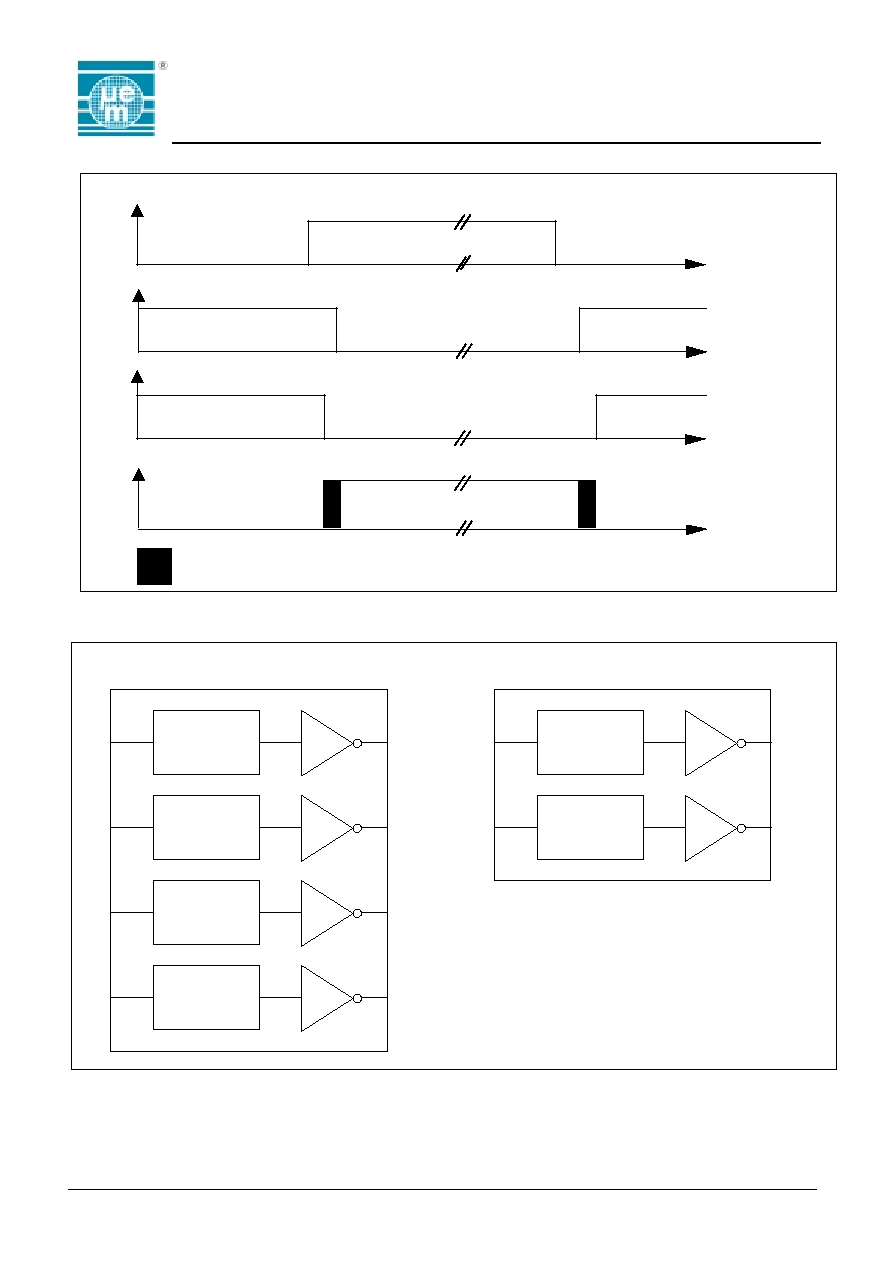
Timing Waveforms
t
t
t
: HIGH IMPEDANCE OUTPUT
t
IN
VGP
VGN
OUT
Fig. 3
Block Diagram
Anti-current
inverter
IN1
Anti-current
inverter
IN2
Anti-current
inverter
IN3
Anti-current
inverter
IN4
OUT1
OUT2
OUT3
OUT4
Anti-current
inverter
IN1
Anti-current
inverter
IN2
OUT1
OUT2
Version V2
Version V1
Fig. 4

EM5060
Copyright
2002, EM Microelectronic-Marin SA
4
www.emmicroelectronic.com
Functional Description
ANTI-CURRENT
INVERTER
V
DD
V
SS
Out
VGP
VGN
In
Fig. 5
Chip Information
H5060 v1
VDD
OUT
1
OUT
2
OUT
3
OUT
4
IN1
IN2
IN3
IN4
VSS
X=19, Y=98
0
X=294
X=541
X=819
X=1066
X=65
X=312
X=590
X=837
X=1082, Y=0
HIZ
X=0,
Y=508
X=-160
Y=-171
H5060 v2
VDD
NC
OUT
1
OUT
2
NC
NC
IN1
IN2
NC
VSS
X=19, Y=9
8
X=294
X=541
X=819
X=1066
X=65
X=312
X=590
X=837
X=1082, Y=0
HIZ
X=0,
Y=508
X=-160
Y=-171
NOTE: The origin (0,0) is the lower left coordinate of center pads
The lower left corner of the chip shows distances
N.C.
Not connected
All dimensions in microns
Fig. 6
Ordering Information
EM5060 is available in two versions:
∑
Version
V1
contains four input/outputs (INPUTS = IN1, IN2, IN3, IN4 ; OUTPUTS = OUT1, OUT2, OUT3, OUT4).
∑
Version
V2
contains two input/outputs (INPUTS = IN1, IN2 ; OUTPUTS = OUT1, OUT2).
When ordering, please specify the complete Part Number below.
Part Number
Version
Die & Delivery Form
EM5060V1WP11
V1
Die in waffle pack, 11 mils thickness
EM5060V1WS11
V1
Sawn wafer, 11 mils thickness
EM5060V2WP11
V2
Die in waffle pack, 11 mils thickness
EM5060V2WS11
V2
Sawn wafer, 11 mils thickness
EM Microelectronic-Marin SA cannot assume responsibility for use of any circuitry described other than circuitry entirely
embodied in an EM Microelectronic-Marin SA product
EM Microelectronic-Marin SA reserves the right to change the specifications without notice at any time. You are strongly
urged to ensure that the information given has not been superseded by a more up to date version.
© 2002 EM Microelectronic-Marin SA, 05/02 Rev. B/481
EM5060 V1
EM5060 V2