 | –≠–ª–µ–∫—Ç—Ä–æ–Ω–Ω—ã–π –∫–æ–º–ø–æ–Ω–µ–Ω—Ç: EM6152A50 | –°–∫–∞—á–∞—Ç—å:  PDF PDF  ZIP ZIP |
Document Outline
- ˛ˇ
- ˛ˇ
- ˛ˇ
- ˛ˇ
- ˛ˇ
- ˛ˇ
- ˛ˇ
- ˛ˇ
- ˛ˇ
- ˛ˇ
- ˛ˇ
- ˛ˇ
- ˛ˇ
- ˛ˇ

R
EM6152A
Copyright © 2006, EM Microelectronic-Marin SA
1
www.emmicroelectronic.com
06/06, rev. B, Prelim.
5V Automotive Regulator with Windowed Watchdog
Description
The EM6152A offers a high level of integration by combining
voltage regulation, voltage monitoring and software
monitoring using a windowed watchdog.
A comparator monitors the voltage applied at the V
IN
input
comparing it with an internal voltage reference V
REF
. The
power-on reset function is initialized after V
IN
reaches V
REF
and takes the reset output inactive after a delay T
POR
depending on external resistance R
OSC
. The reset output goes
active low when the V
IN
voltage is less than V
REF
. The
RES
and
EN
outputs are guaranteed to be in a correct state for a
regulated output voltage as low as 1.2 V. The watchdog
function monitors software cycle time and execution.
If software clears the watchdog too quickly (incorrect cycle
time) or too slowly (incorrect execution) it will cause the
system to be reset. For enhanced security, the watchdog
must be serviced within an "open" time window. During the
remaining time, the watchdog time window is "closed" and a
reset will occur should a
TCL
pulse be received by the
watchdog during this "closed" time window. The ratio of the
open/closed window is either 33%/67% or 67%/33%.
The system ENABLE output prevents critical control functions
being activated until software has successfully cleared the
watchdog three times. Such a security could be used to
prevent motor controls being energized on repeated resets of
a faulty system.
When the microcontroller goes in stand-by mode or stops
working, no signal is received on the
TCL
input of the
EM6152A (version 55) and it goes into a stand-by mode in
order to save power (CAN-bus sleep detector).
In EM6152A, the voltage regulator has a low dropout voltage
and a low quiescent current of 90
A. The quiescent current
increases only slightly in dropout prolonging battery life. Built-
in protection includes a positive transient absorber for up to
45 V (load dump) and the ability to survive an unregulated
input voltage of -42 V (reverse battery). The input may be
connected to ground or to a reverse voltage without reverse
current flowing from the output to the input.
Features
Low quiescent current 90
A
-40∞C to +125∞C temperature range
Highly accurate 5 V, 150 mA guaranteed output (actual
maximum current depends on power dissipation)
Low dropout voltage, typically 250 mV at 100 mA
Unregulated DC input can withstand -42 V reverse battery
and +45 V power transients
Fully operational for unregulated DC input voltage up to
40 V and regulated output voltage down to 3.5 V
No reverse output current
Very low temperature coefficient for the regulated output
Current
limiting
Windowed watchdog with an adjustable time windows,
guaranteeing a minimum time and a maximum time
between software clearing of the watchdog
Time base accuracy
±8% (at 100ms)
Sleep mode function (V55)
Adjustable threshold voltage using external resistors
Adjustable power on reset (POR) delay using one
external resistor
Open-drain active-low RESET output
Reset output guaranteed for regulated output voltage
down to 1.2 V
System ENABLE output offers added security
Qualified according to AEC-Q100
Pin out compatible with EM6152
Green SO-8 and Exposed Pad SO-16 packages (RoHS
compliant)
Applications
Automotive
systems
Industrial
Home
security
systems
Telecom / Networking
Computers
Set top boxes
Typical Operating Configuration
Fig.
1
Selection Table
Part Number
V
REF
Closed
Window
Open
Window
CAN-bus sleep
detector
EM6152A
30
1.17
V
67%
33%
NO
EM6152A
50
1.52
V
67%
33%
NO
EM6152A
53
1.52
V
33%
67%
NO
EM6152A
55
1.275
V
67%
33%
YES
Please refer to Fig. 4 for more information about the
open/closed window of the watchdog.
EM MICROELECTRONIC -
MARIN SA
5V
+
V
SS
GND
Unregulated
Voltage
INPUT
OUTPUT
EM6152A
RES
EN
TCL
V
IN
Micr
op
roc
e
ss
or
V
DD
I/O
RES
I/O
R
OSC
10uF
100nF
22uF
R
OSC
R
1
R
2
+
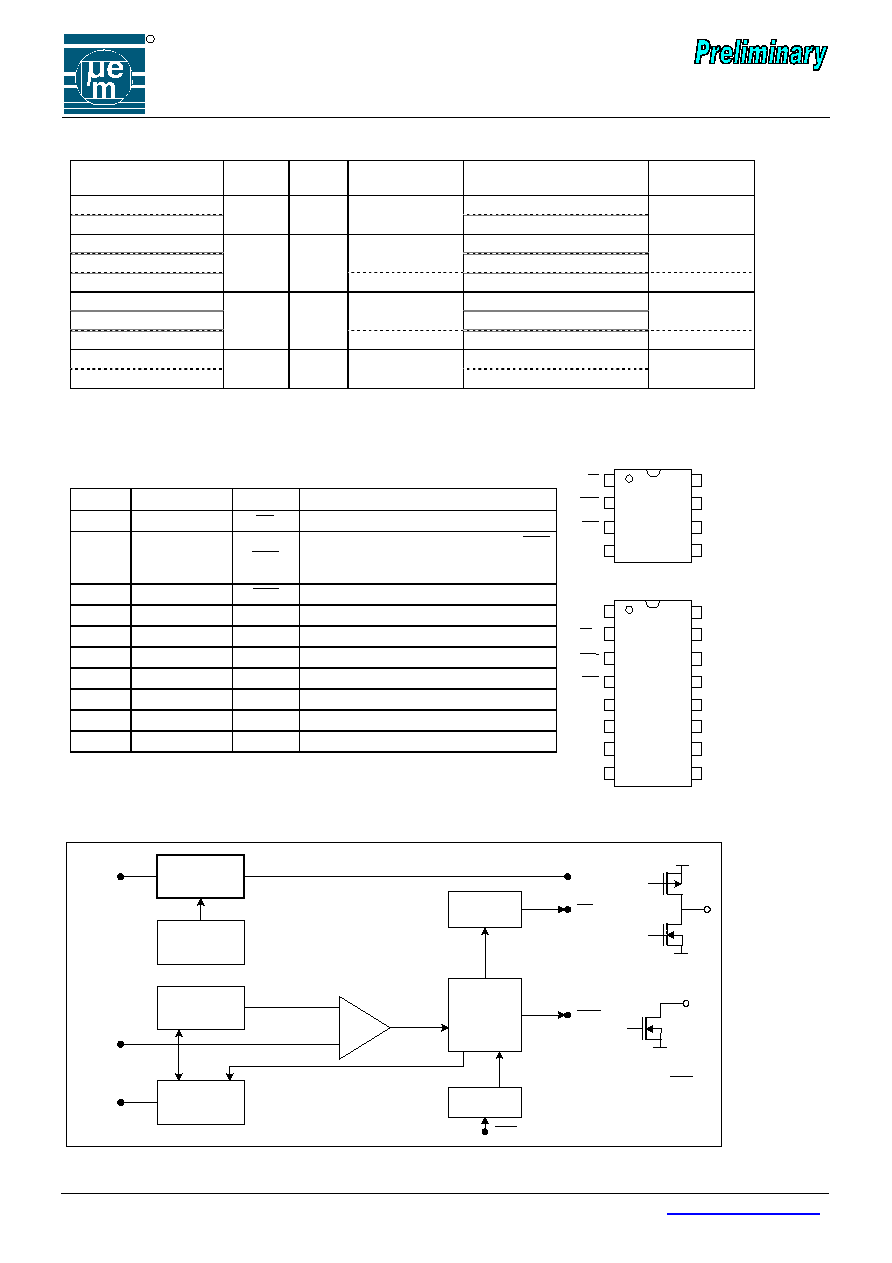
R
EM6152A
Copyright © 2006, EM Microelectronic-Marin SA
2
www.emmicroelectronic.com
06/06, rev. B, Prelim.
Ordering Information
Note: the "+" symbol at the end of the part number means that this product is RoHS compliant (green). For version V30, please
contact EM Microelectronic.
Pin Assignment and Description
SO8
Ex. Pad SO-16
Name
Function
1 2 EN
Push-pull active low enable output
2 3 RES
Open drain active low reset output. RES
must be pulled up to V
OUTPUT
even if
unused
3 4 TCL
Watchdog timer clear input signal
4 5 V
SS
GND
terminal
5
12
INPUT
Voltage regulator input
6
13
OUTPUT Voltage regulator output
7 14
R
OSC
R
OSC
input for RC oscillator tuning
8 15 V
IN
Voltage comparator input
-
1, 6 to 11, 16
NC
No connect
-
Exposed pad
Can be connected to V
SS
or left floating
Block Diagram EM6152A
RES
EN
TCL
Voltage
Regulator
Voltage
Reference
Voltage
Reference
Current
Controlled
Oscillator
-
+
V
REF
Comparator
Reset
Control
Timer
Enable
Logic
INPUT
V
IN
R
OSC
OUTPUT
Open drain
output RES
Fig. 3
Part Number
Version
V
REF
Package
Delivery
Form
Package
Marking
EM6152A30SO8A+
Stick, 97 pcs
EM6152A30SO8B+
V30 1.170
V
SO-8
Tape & Reel, 2500 pcs
6152A30
EM6152A50SO8A+
Stick, 97 pcs
EM6152A50SO8B+
SO-8
Tape & Reel, 2500 pcs
6152A50
EM6152A50ES16B+
V50
1.52 V
Ex. Pad SO-16
Tape & Reel, 2500 pcs
EM6152A050
EM6152A53SO8A+
Stick, 97 pcs
EM6152A53SO8B+
SO-8
Tape & Reel, 2500 pcs
6152A53
EM6152A53ES16B+
V53
1.52V
Ex. Pad SO-16
Tape & Reel, 2500 pcs
EM6152A053
EM6152A55SO8A+
Stick, 97 pcs
EM6152A55SO8B+
V55 1.275
V
SO-8
Tape & Reel, 2500 pcs
6152A55
V
SS
R
OSC
4
OUTPUT
INPUT
RES
EN
TCL
V
IN
SO8
1
3
2
8
6
7
5
EM6152A
V
SS
R
OSC
OUTPUT
INPUT
RES
EN
TCL
V
IN
Ex. Pad SO-16
EM6152A
NC
NC
NC
NC
16
15
14
13
12
11
10
9
1
2
3
4
5
6
7
8
NC
NC
NC
NC
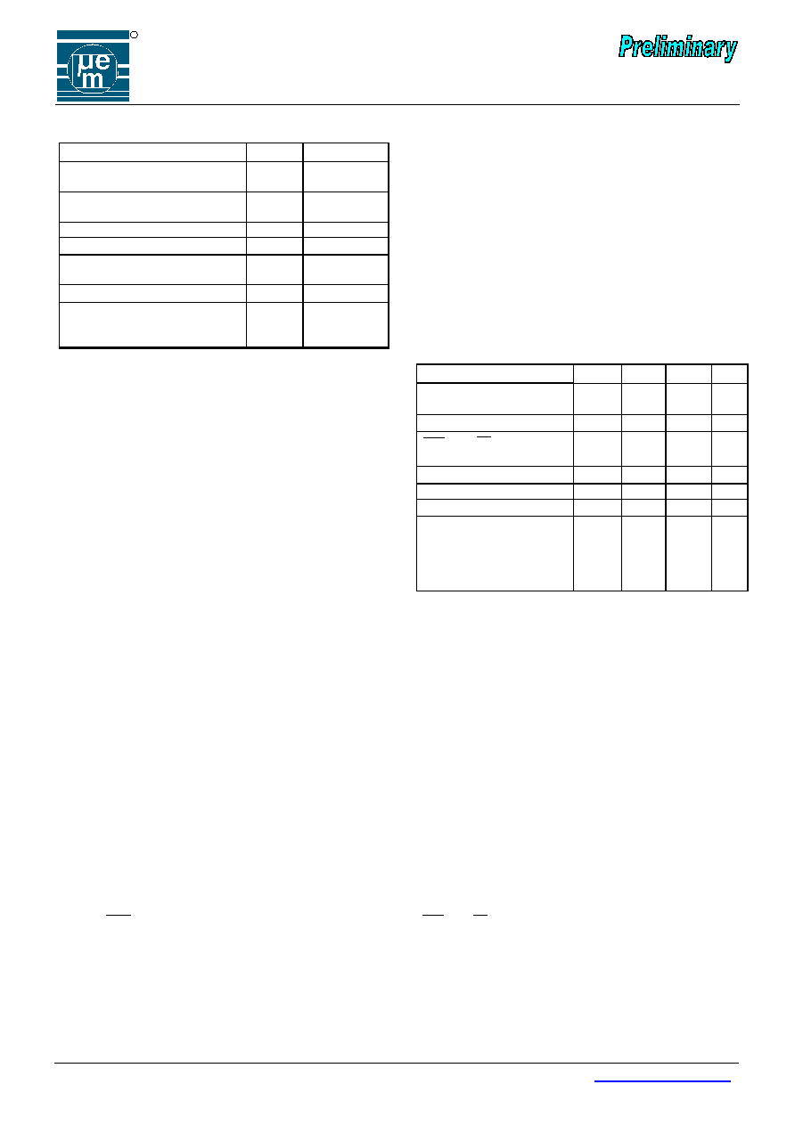
R
EM6152A
Copyright © 2006, EM Microelectronic-Marin SA
3
www.emmicroelectronic.com
06/06, rev. B, Prelim.
Absolute Maximum Ratings
Parameter Symbol
Conditions
Continuous voltage at INPUT
to V
SS
V
INPUT
-0.3 to +40V
Transients on INPUT for
t < 100 ms and duty cycle 1%
V
TRANS
Up to +45V
Max. voltage at any signal pin
V
MAX
V
OUTPUT
+ 0.3V
Min. voltage at any signal pin
V
MIN
V
SS
≠ 0.3V
Reverse supply voltage on
INPUT
V
REV
-42V
Storage temperature
T
STO
-65 to +150 ∞C
ESD
According to MIL-STD-883
method 3015.7
V
Smax
2000V
Table 1
Stresses above these listed maximum ratings may cause
permanent damages to the device. Exposure beyond
specified operating conditions may affect device reliability or
cause malfunction.
Decoupling Methods
The input capacitor is necessary to compensate the line
influences. A resistor of approx. 1
connected in series
with the input capacitor may be used to damp the oscillation
of the input capacitor and input inductance. The ESR value
of the capacitor plays a major role regarding the efficiency of
the decoupling. It is recommended also to connect a
ceramic capacitor (100 nF) directly at the IC's pins. In
general the user must assure that pulses on the input line
have slew rates lower than 1 V/µs. On the output side, the
capacitor is necessary for the stability of the regulation
circuit. The stability is guaranteed for values of 10 µF or
greater. It is especially important to choose a capacitor with
a low ESR value. Tantalum capacitors are recommended.
See the notes related to Table 2. Special care must be
taken in disturbed environments (automotive, proximity of
motors and relays, etc.).
Handling Procedures
This device has built-in protection against high static
voltages or electric fields; however, it is advised that normal
precautions be taken as for any other CMOS component.
Unless otherwise specified, proper operation can only occur
when all terminal voltages are kept within the voltage range.
At any time, all inputs must be tied to a defined logic voltage
level.
Operating Conditions
Parameter
Symbol Min. Max.
Units
Operating junction
temperature
T
j
-40
+125
∞C
INPUT voltage (note 1, 2)
V
INPUT
5.5 40 V
RES
and
EN
guaranteed
(note 3)
V
OUTPUT
1.2
V
OUTPUT current (note 4)
I
OUTPUT
150 mA
Comparator input voltage
V
IN
0
V
OUTPUT
V
RC-oscillator programming R
OSC
10 1000 k
Package thermal resistance
from junction to ambient :
SO-8
Exp. Pad SO-16 150 MILS
(note 5)
R
th(j-a)
30
160
90
∞C/W
Table 2
Note 1: full operation guaranteed. To achieve the load regulation specified in Table 3 a 22
F capacitor or greater is required on the INPUT,
see Fig. 1b. The 22
F must have an effective resistance
4
and a resonant frequency above 500 kHz.
Note 2: a
10
F load capacitor and a 100 nF decoupling capacitor are required on the regulator OUTPUT for stability. The 10
F must have
an effective series resistance of
4
and a resonant frequency above 500 kHz.
Note 3:
RES
must be pulled up externally to V
OUTPUT
even if it is unused. ( RES and EN
are used as inputs by EM test)
Note 4: the OUTPUT current will not apply to the full range of input voltage. Power dissipation that would require the EM6152A to work above
the maximum junction temperature (+125∞C) must be avoided.
Note 5: the thermal resistance specified assumes the package is soldered to a PCB. A typical value of 51∞C/W has been obtained with a dual
layer board, with the slug soldered to the heat-sink area of the PCB (See Figure 16)

R
EM6152A
Copyright © 2006, EM Microelectronic-Marin SA
4
www.emmicroelectronic.com
06/06, rev. B, Prelim.
Electrical Characteristics
V
INPUT
= 13.5 V, C
L
= 10
F + 100 nF, C
INPUT
= 22
F, T
j
= -40 to +125∞C, unless otherwise specified
Parameter Symbol Test
Conditions
Min.
Typ.
Max.
Unit
Supply current in standby mode and sleep
mode for V55 (note 1)
I
SS
R
OSC
= don't care, TCL = V
OUTPUT
,
V
IN
= 0 V, I
L
= 100
A
80
135
A
Supply current (note1)
I
SS
R
OSC
= 100 k
, I/P
S
at V
OUTPUT
,
O/P
S
1 M
to V
OUTPUT
, I
L
= 100
A
90
140
A
Supply current
I
SS
R
OSC
= 100 k
, I/P
S
at V
OUTPUT
,
O/P
S
1 M
to V
OUTPUT
, I
L
= 50 mA
1.7 4 mA
Voltage
regulator
Output voltage
V
OUTPUT
5 mA
I
L
100 mA
4.85
5
5.15
V
Line regulation (note 2)
V
LINE
6 V
V
INPUT
28 V, I
L
= 1 mA
5
30
mV
Load regulation (note 2)
V
L
1
mA
I
L
100 mA, V
INPUT
= 6V
50
95
mV
Dropout voltage (note 3)
V
DROPOUT
I
L
= 100 mA
250
500
mV
Current limit
I
Lmax
OUTPUT tied to V
SS
, V
INPUT
= 6V
150
200
500
mA
Supervisory and watchdog
RES
&
EN
V
OUTPUT
= 4.5 V, I
OL
= 8 mA
0.25
0.45
V
Output Low Voltage
V
OL
V
OUTPUT
= 1.2 V, I
OL
= 0.5 mA
0.04
0.2
V
EN
V
OUTPUT
= 4.5 V, I
OH
= -1 mA
3.5
4.1
V
Output High Voltage
V
OH
V
OUTPUT
= 1.2 V, I
OH
= -20
A 0.9
1.05
V
TCL
Input Low Level
V
IL
V
SS
0.5 V
TCL
Input High Level
V
IH
2.5 V
OUTPUT
V
TCL
Leakage current
I
LI
V
SS
V
TCL
V
OUTPUT
0.05
A
Version V30
1.135 1.170 1.205
V
Comparator reference (note 5, 6)
V
REF
Version V50
1.475 1.520 1.565
V
Version
V53
1.475 1.520 1.565
V
Version V55
1.235 1.275 1.315
V
Comparator hysteresis (note 6)
V
HY
2
mV
V
IN
input resistance
R
VIN
100
M
Table 3
Note 1: if INPUT is connected to V
SS
, no reverse current will flow from the OUTPUT to the INPUT, however the supply current specified will be
sank by the OUTPUT to supply the EM6152A.
Note 2: regulation is measured at constant junction temperature using pulse testing with a low duty cycle. Changes in OUTPUT voltage due to
heating effects are covered in the specification for thermal regulation.
Note 3: the dropout voltage is defined as the INPUT to OUTPUT differential, measured with the input voltage equal to 5.0 V.
Note 4: output voltage temperature coefficient is defined as the change in OUTPUT voltage after a change in power dissipation is applied,
excluding load or line regulation effects.
Note 5: the comparator and the voltage regulator have separate voltage references (see "Block Diagram" Fig. 3).
Note 6: the comparator reference is the power-down reset threshold. The power-on reset threshold equals the comparator reference voltage
plus the comparator hysteresis (see Fig. 5).

R
EM6152A
Copyright © 2006, EM Microelectronic-Marin SA
5
www.emmicroelectronic.com
06/06, rev. B, Prelim.
Timing Characteristics
V
INPUT
= 13.5 V, I
L
= 100
A, C
L
= 10
F + 100 nF, C
INPUT
= 22
F, T
j
= -40 to + 125
∞C, unless otherwise specified
Parameter Symbol Test
Conditions
Min.
Typ.
Max.
Units
Propagation delay TCL to Output Pins
T
DIDO
250 500 ns
V
IN
sensitivity
T
SEN
V
INhigh
=1.1
x
V
REF
, V
INlow
=0.9
x
V
REF
0.5 3 15
s
Watchdog Reset Pulse Period
T
WDRP
TCL
inactive
T
CW
+ T
OW
+ T
WDR
ms
Version V30
Power-on Reset delay
T
POR
R
OSC
= 116.9 k
±1% 91.6
100
108.3
Closed Window Time
T
CW
74 80 85.76
Open Window Time
T
OW
37 40 42.88
ms
Watchdog Time
T
WD
92.5 100 107.2
Watchdog Reset Pulse Width if no TCL
T
WDR
2.25 2.5 2.75
Version V50
Power-on Reset delay
T
POR
R
OSC
= 121.6 k
±1% 91.6
100
108.3
Closed Window Time
T
CW
74 80 85.76
Open Window Time
T
OW
37 40 42.88
ms
Watchdog Time
T
WD
92.5 100 107.2
Watchdog Reset Pulse Width if no TCL
T
WDR
2.25 2.5 2.75
Version V53
Power-on Reset delay
T
POR
R
OSC
= 23.2 k
±1%
4.57 5.0 5.44
Closed Window Time
T
CW
9.24 10 10.77
Open Window Time
T
OW
18.48 20 21.54
ms
Watchdog Time
T
WD
18.48 20 21.54
Watchdog Reset Pulse Width if no TCL
T
WDR
0.56 0.625 0.69
Version V55
Power-on Reset delay
T
POR
R
OSC
= 107.5 k
±1% 91.6
100
108.3
Closed Window Time
T
CW
74 80 85.76
Open Window Time
T
OW
37 40 42.88
Watchdog Time
T
WD
92.5 100 107.2
ms
Watchdog Reset Pulse Width if no TCL
T
WDR
2.25 2.5 2.75
Watchdog Reset Pulse Width in Sleep Mode
T
WDRS
R
OSC
off; R
INT
=1M
2.8 3.2 3.6
Watchdog Reset Pulse Period in Sleep Mode
T
WDRPS
TCL inactive
750
1100 1450
Table 4
For different values of T
WD
and R
OSC
, see figures 9 to 12.
Timing Waveforms
Watchdog Timeout Period
Fig. 4
T
CW
(closed window)
T
OW
(open)
T
WD
80
120
Time [ms]
Watchdog
timer reset
( V30, V50 and V55 have similar ratios for T
CW
and T
OW
)
Version V50:
T
CW
(closed)
T
OW
(open)
10
30
Time [ms]
Watchdog
timer reset
Version V53:
For R
OSC
=121.6 kOhm
For R
OSC
=23.2 kOhm
T
WD