
EM6353
Copyright
© 2006, EM Microelectronic-Marin SA
03/06 ≠ rev.K
1
www.emmicroelectronic.com
Reset Circuit with Fixed Delay
Description
The EM6353 is an ultra-low current reset circuit available in a
large variety of configurations and very small packages for
maximum flexibility in all end-applications up to 125∞C and
using power supplies between 1.5V and 5.5V.
This circuit monitors the supply voltage of any electronic
system, and generates the appropriate reset signal after a
fixed reset timeout period. The threshold defines the
minimum allowed voltage which guarantees the good
functionality of the system. When V
DD
rises above V
TH
, the
output remains active for an additional delay time. This
allows the system to stabilize before getting fully active.
The EM6353 features three output types: active-low push-
pull, active-low open-drain and active-high push-pull.
Small SC70-5L and SOT23-3L packages as well as ultra-low
supply current of 2.9µA make the EM6353 an ideal choice
for portable and battery-operated devices.
Typical Application
V
DD
GND
RESET
EM6353
V
DD
GND
RESET
MPU, DSP
V
DD
GND
*
R
EXT
for open-drain version only
*
Pin Configuration
(top view)
SOT23-3L
"alpha" bonding
1
3
1
2
3
GND
V
DD
SOT23-3L
"beta" bonding
RESET
(RESET)
SC70-5L
(compatible with SC70-3 by rotating 180∞)
1
5
V
DD
RESET
(RESET)
3
NC
1
2
3 GND
V
DD
RESET
(RESET)
4
2 V
DD
RESET
(RESET)
5
GND
NC
NC
NC
4
2
GND
Features
!
200ms reset timeout period (25ms on request)
!
Ultra-low supply current of 2.9µA (V
DD
=3.3V)
!
Operating temperature range: -40∞C to +125∞C
!
±1.5% reset threshold accuracy
!
11 reset threshold voltages V
TH
: 4.63V, 4.4V, 3.08V,
2.93V, 2.63V, 2.2V, 1.8V, 1.66V, 1.57V, 1.38V, 1.31V
!
3 reset output options:
"
Active-low
RESET
push-pull
"
Active-low
RESET
open-drain
"
Active-high
RESET
push-pull
!
No external components
!
Immune to short negative V
DD
transients
!
Guaranteed Reset valid down to 0.8V
!
Threshold hysteresis: 2.1% of V
TH
!
Very small SOT23-3L and SC70-5L packages
Applications
!
Mobile phones
!
Set-top boxes
!
Video, digital cameras, DVD players and recorders
!
Modems
!
Personal computers
!
Switching hubs
!
Copiers and fax
!
Utility meters
!
Automotive systems
Block Diagram
RESET
V
DD
GND
+
-
Voltage
Reference
Reset
Logic
RESET
Oscillator
Pin Description
Pin
SOT23-3L
"beta"
SOT23-3L
"alpha"
SC70-5L
Name
Function
1 3
4
GND
Ground
RESET
Active-low RESET output. RESET remains low for the reset timeout period
after all reset conditions are deasserted and then goes high.
2 1
5
RESET
Active-high RESET output. RESET remains high for the reset timeout period
after all reset conditions are deasserted and then goes low.
3 2
2 V
DD
Supply Voltage (5.5V max.)
-
-
1,3
N.C.
Not connected. Not internally connected.
EM MICROELECTRONIC
- MARIN SA

EM6353
Copyright
© 2006, EM Microelectronic-Marin SA
03/06 ≠ rev.K
2
www.emmicroelectronic.com
Ordering Information
EM6353
-
Delay (t
POR
):
RoHS Compliance:
B = 200ms
+ = lead-free/green mold compliant
A = 25ms
[blank] = leaded
Reset Output Type:
Reset Threshold Voltage (V
TH
):
X = Active-low /RES push-pull
1.3 = 1.31V
2.6 = 2.63V
Y = Active-low /RES open-drain
1.4 = 1.38V
2.9 = 2.93V
Z = Active-high RES push-pull
1.6 = 1.57V
3.1 = 3.08V
1.7 = 1.66V
4.4 = 4.40V
Package & Bonding:
1.8 = 1.80V
4.6 = 4.63V
1SP3B = SOT23-3, "alpha", Tape&Reel 3kpcs
2.2 = 2.20V
2SP3B = SOT23-3, "beta", Tape&Reel 3kpcs
SC5B = SC70-5, Tape&Reel 3kpcs
B X
2.9 +
2SP3B
Note: Subject to availability (see standard versions list below). Please give complete Part Number when ordering. All
parts are offered in tape-and-reel only (3000 units).
Standard Versions (Top Marking)
1)
Top marking is the standard from 2006. No bottom marking exists. Where ## refers to the lot number (EM internal
reference only)
2)
Top marking with 4 characters is standard from 2003. For lead-free/green mold (RoHS) parts, the first letter of top
marking with 4 characters begins with letter "B" instead of letter "A". Bottom marking indicates the lot number.
Part Number
Top
Marking
1)
Top Marking
2)
with 4
Characters
EM6353BX1SP3B-1.3
ALBA
EM6353BX1SP3B-2.6
ALBG
EM6353BX1SP3B-2.6+
BLBG
EM6353BX1SP3B-2.9
ALBH
EM6353BX1SP3B-2.9+ C1## BLBH
EM6353BX1SP3B-4.4
ALBK
EM6353BX1SP3B-4.4+ C2## BLBK
EM6353BX1SP3B-4.6
ALBL
EM6353BX1SP3B-4.6+
BLBL
EM6353BX2SP3B-1.3
ALWA
EM6353BX2SP3B-1.8
ALWE
EM6353BX2SP3B-1.8+
BLWE
EM6353BX2SP3B-2.6 AW## ALWG
EM6353BX2SP3B-2.6+ BW## BLWG
EM6353BX2SP3B-2.9 AR## ALWH
EM6353BX2SP3B-2.9+ BR## BLWH
EM6353BX2SP3B-3.1 PC## ALWJ
EM6353BX2SP3B-3.1+ C5## BLWJ
EM6353BX2SP3B-4.4
ALWK
EM6353BX2SP3B-4.4+ C8## BLWK
EM6353BX2SP3B-4.6
ALWL
EM6353BX2SP3B-4.6+
BLWL
EM6353BXSC5B-1.3
ALWA
EM6353BXSC5B-1.8
ALWE
EM6353BXSC5B-2.6 AW## ALWG
EM6353BXSC5B-2.6+ BW## BLWG
EM6353BXSC5B-2.9 AR## ALWH
EM6353BXSC5B-3.1 PC## ALWJ
Part Number
Top
Marking
1)
Top Marking
2)
with 4
Characters
EM6353BXSC5B-3.1 C5## BLWJ
EM6353BXSC5B-4.6
ALWL
EM6353BY1SP3B-2.2
ALBS
EM6353BY1SP3B-2.6
ALBT
EM6353BY1SP3B-2.9 AS## ALBU
EM6353BY1SP3B-2.9+ BS## BLBU
EM6353BY1SP3B-3.1
ALBV
EM6353BY1SP3B-4.4
ALBW
EM6353BY1SP3B-4.6
ALBX
EM6353BY2SP3B-2.6
ALWT
EM6353BY2SP3B-2.6+ C9## BLWT
EM6353BY2SP3B-2.9
ALWU
EM6353BY2SP3B-2.9+ C7## BLWU
EM6353BY2SP3B-3.1
ALWV
EM6353BY2SP3B-3.1+
BLWV
EM6353BY2SP3B-4.4
ALWW
EM6353BY2SP3B-4.6
ALWX
EM6353BY2SP3B-4.6+
BLWX
EM6353BYSC5B-2.9
ALWU
EM6353BYSC5B-2.9+ C7## BLWU
EM6353BYSC5B-4.4
ALWW
EM6353BZ2SP3B-2.9 AV## ALW6
EM6353BZ2SP3B-2.9+ BV## BLW6
EM6353BZ2SP3B-3.1
ALW7
EM6353BZ2SP3B-3.1+
BLW7
EM6353BZ2SP3B-4.6
ALW9
EM6353BZ2SP3B-4.6+ CB## BLW9

EM6353
Copyright
© 2006, EM Microelectronic-Marin SA
03/06 ≠ rev.K
3
www.emmicroelectronic.com
Standard Versions (samples)
Part Number
EM6353BX1SP3B-2.6+
EM6353BX1SP3B-2.9+
EM6353BX1SP3B-4.4+
EM6353BX1SP3B-4.6+
EM6353BX2SP3B-1.8+
EM6353BX2SP3B-2.6+
EM6353BX2SP3B-2.9+
EM6353BX2SP3B-3.1+
EM6353BX2SP3B-4.4+
EM6353BX2SP3B-4.6+
Part Number
EM6353BXSC5B-2.9
EM6353BXSC5B-3.1
EM6353BY1SP3B-2.9+
EM6353BY2SP3B-2.9+
EM6353BY2SP3B-3.1+
EM6353BY2SP3B-4.6+
EM6353BYSC5B-2.9+
EM6353BZ2SP3B-2.9+
EM6353BZ2SP3B-3.1+
EM6353BZ2SP3B-4.6
Sample stock is generally held on
standard versions only. Non standard versions have a 30,000 pieces minimum order
quantity. Please contact factory for other versions not shown here and for availability of non standard versions.
Absolute Maximum Ratings
Parameter Symbol
Conditions
Voltage at V
DD
to GND
V
DD
-0.3V to +6V
Minimum voltage at any signal pin
V
MIN
GND
-
0.3V
Maximum voltage at any signal pin
V
MAX
V
DD
+ 0.3V
Electrostatic discharge max. to
MIL-STD-883C method 3015.7
with ref. to V
SS
V
ESD
2000V
Max. soldering conditions
T
MAX
250∞C
x
10s
Storage Temperature Range
T
STG
-65∞C to +150∞C
Stresses above these listed maximum ratings may cause
permanent damage to the device. Exposure beyond
specified operating conditions may affect device
reliability or cause malfunction.
Handling Procedures
This device has built-in protection against high static
voltages or electric fields; however, anti-static
precautions must be taken as for any other CMOS
component. Unless otherwise specified, proper operation
can only occur when all terminal voltages are kept within
the voltage range. Unused inputs must always be tied to
a defined logic voltage level.
Operating Conditions
Parameter Symbol
Min
Max
Unit
Supply voltage (note 1)
V
DD
0.8 5.5
V
Operating Temperature
T
A
-40
+125 ∞C
Electrical Characteristics
Unless otherwise specified: V
DD
= 0.8V to 5.5V, T
A
=-40∞C to +125∞C (note 1).
Parameter Symbol
Conditions
Min
Typ
Max
Unit
+25∞C -
4.6
V
DD
=1.5V
-40∞C to +125∞C
-
2.3
7
+25∞C -
5.5
V
DD
=3.3V
-40∞C to +125∞C
-
2.9
8.3
+25∞C -
6.3
Supply current (note 2)
I
DD
V
DD
=5.0V
-40∞C to +125∞C
-
3.4
9.6
µA
+25∞C 1.290
1.330
-40∞C to +85∞C
1.245
1.382
EM6353 ≠ 1.3
-40∞C to +125∞C
1.221
1.31
1.387
+25∞C 1.359
1.401
-40∞C to +85∞C
1.311
1.456
EM6353 ≠ 1.4
-40∞C to +125∞C
1.286
1.38
1.461
+25∞C 1.546
1.594
-40∞C to +85∞C
1.492
1.656
EM6353 ≠ 1.6
-40∞C to +125∞C
1.463
1.57
1.663
+25∞C 1.635
1.685
-40∞C to +85∞C
1.577
1.751
EM6353 ≠ 1.7
-40∞C to +125∞C
1.547
1.66
1.758
+25∞C 1.773
1.827
-40∞C to +85∞C
1.710
1.899
EM6353 ≠ 1.8
-40∞C to +125∞C
1.678
1.80
1.906
+25∞C 2.167
2.233
-40∞C to +85∞C
2.090
2.321
EM6353 ≠ 2.2
-40∞C to +125∞C
2.050
2.20
2.330
+25∞C 2.591
2.669
Threshold voltage
(note 3)
V
TH
EM6353 ≠ 2.6
-40∞C to +85∞C
2.499
2.63
2.775
V

EM6353
Copyright
© 2006, EM Microelectronic-Marin SA
03/06 ≠ rev.K
4
www.emmicroelectronic.com
-40∞C to +125∞C
2.451
2.785
+25∞C 2.886
2.974
-40∞C to +85∞C
2.784
3.091
EM6353 ≠ 2.9
-40∞C to +125∞C
2.731
2.93
3.103
+25∞C 3.034
3.126
-40∞C to +85∞C
2.926
3.249
EM6353 ≠ 3.1
-40∞C to +125∞C
2.871
3.08
3.262
+25∞C 4.334
4.466
-40∞C to +85∞C
4.180
4.642
EM6353 ≠ 4.4
-40∞C to +125∞C
4.101
4.40
4.660
+25∞C 4.561
4.699
-40∞C to +85∞C
4.399
4.885
EM6353 ≠ 4.6
-40∞C to +125∞C
4.315
4.63
4.903
Threshold hysteresis
V
HYS
T
A
=+25∞C -
2.1%
∑V
TH
- V
Note 1: Production tested at +25∞C only. Over temperature limits are guaranteed by design, not production tested.
V
DD
min=0.9V for active-high versions (EM6353_Z).
Note 3: Threshold voltage is specified for V
DD
falling.
EM6353
Copyright
© 2006, EM Microelectronic-Marin SA
03/06 ≠ rev.K
5
www.emmicroelectronic.com
Electrical Characteristics
(continued)
Unless otherwise specified: V
DD
= 0.8V to 5.5V, T
A
=-40∞C to +125∞C (note 1).
Parameter Symbol Conditions Min
Typ
Max
Unit
EM6353B 155
200
224
Reset timeout period
t
POR
V
DD
from 0V to V
TH (typ)
+15%
(note 2 and 4). T
A
= +25∞C
EM6353A 19.4
25 28
ms
Propagation delay time
V
DD
to
RESET
(RESET) delay
t
P
V
DD
drops from V
TH (typ)
+0.2V to V
TH (typ)
-0.2V
(note 2). T
A
= +25∞C
2 130
255
µs
V
DD
>1V
I
OL
=100
µA
- - 0.3
V
DD
>2.5V I
OL
=1.5mA -
-
0.3
Open-drain RESET output
Voltage
V
OL
V
DD
>5V I
OL
=3mA -
-
0.3
V
V
DD
>1V
I
OL
=100
µA
- - 0.3
V
DD
>2.5V I
OL
=1.5mA -
-
0.3
V
OL
V
DD
>5V I
OL
=3mA -
-
0.35
V
DD
>1V
I
OH
=-30
µA
0.8 - -
V
DD
>2.5V I
OH
=-1.5mA 2
-
-
Push-pull RESET /
RESET
Output voltage
V
OH
V
DD
>5V
I
OH
=-3mA 4
-
-
V
Output leakage current
I
LEAK
Only for EM6353_Y (open-drain)
-
-
0.5
µA
Note 1: Production tested at +25∞C only. Over temperature limits are guaranteed by design, not production tested.
V
DD
min=0.9V for active-high versions (EM6353_Z).
Note 2:
RESET
(RESET) open.
Note 4: Standard version is EM6353B (t
POR
=200ms), available at all times. EM6353A (t
POR
=25ms) is available by mask option and upon
minimum order quantity. Please contact EM sales.
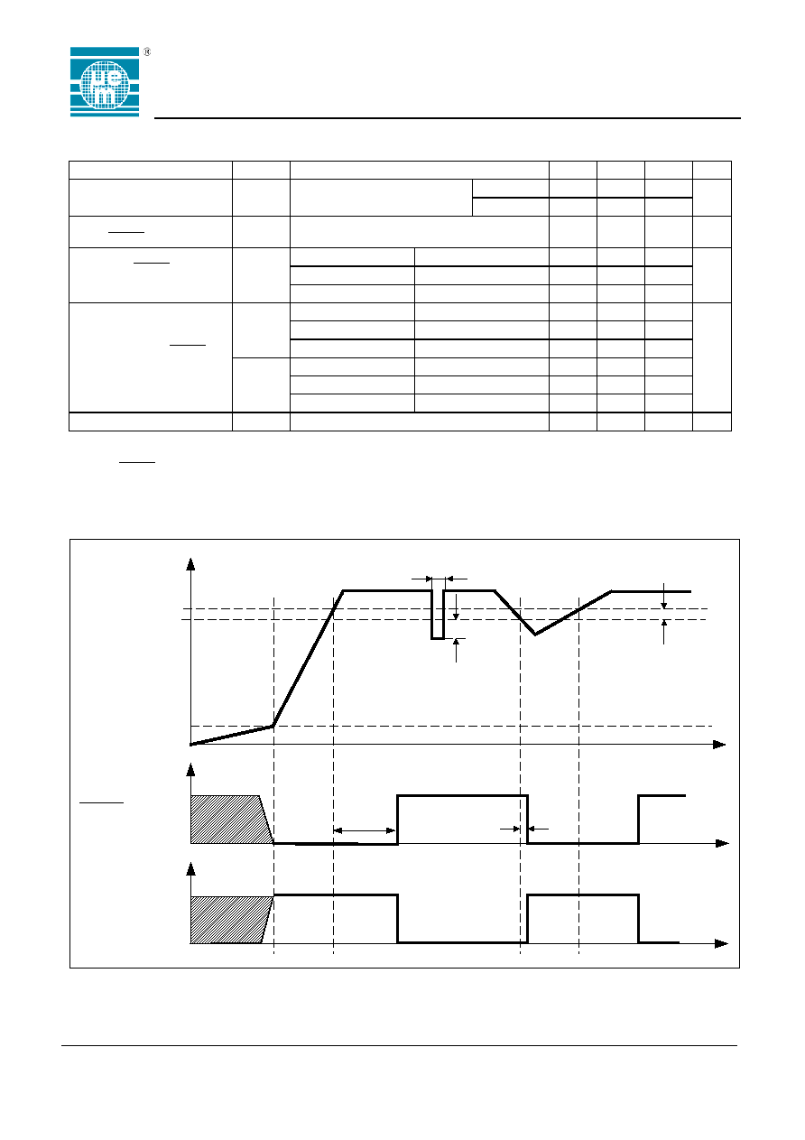
Timing Waveforms
Note 6: t
SEN
= Maximum Transient Duration. Please refer to figure on next page.
Note 7: Overdrive = V
TH-
-V
DD
. Please refer to figure on next page.
RESET
V
DD
0.8V
V
TH
t
t
logic "1"
logic "0"
t
SEN
t
logic "1"
logic "0"
RESET
t
POR
t
P
V
HYS
RESET
Overdrive