EM6640
03/02 REV. C/446
Copyright
2002, EM Microelectronic-Marin SA
1
www.emmicroelectronic.com
Low Power Microcontroller
with EEPROM AND RC Oscillator
Features
∑ Low Power - 42µA active mode
- 8µA standby mode
- 0.3µA sleep mode
@ 3.0V, 600kHz, 25∞C, typ
∑ Voltage Range - 1.9 to 5.5 V
∑ Supply voltage level detection (SVLD)
∑ ROM
-
1280
◊ 16 bit
∑ RAM
-
80
◊ 4 bit
∑ EEPROM
- 32 x 8 bit
∑ 2 clocks per instruction cycle
∑ 72 basic instructions
∑ RC
oscillator
∑ Oscillation detection circuit / Digital watchdog
timer reset.
∑ Maximum 12 inputs (3 ports)
∑ Maximum 8 outputs (2 ports)
∑ Serial Write Buffer - 256 bits (SWB)
∑ 10 bit up/down counter with PWM capability
∑ Frequency out 600kHz, 37.5kHz, 2.3kHz, PWM
∑ Sleep Counter Reset (SCR) programmable.
∑ 8 internal interrupt sources (3◊prescaler,
2
◊timer ,1xSWB, 1◊SVLD, 1xEEPROM)
∑ 4 external interrupt sources (port A)
∑ Reset with input combinations
∑ Packages available : TSSOP16, SO16, SO18
Description
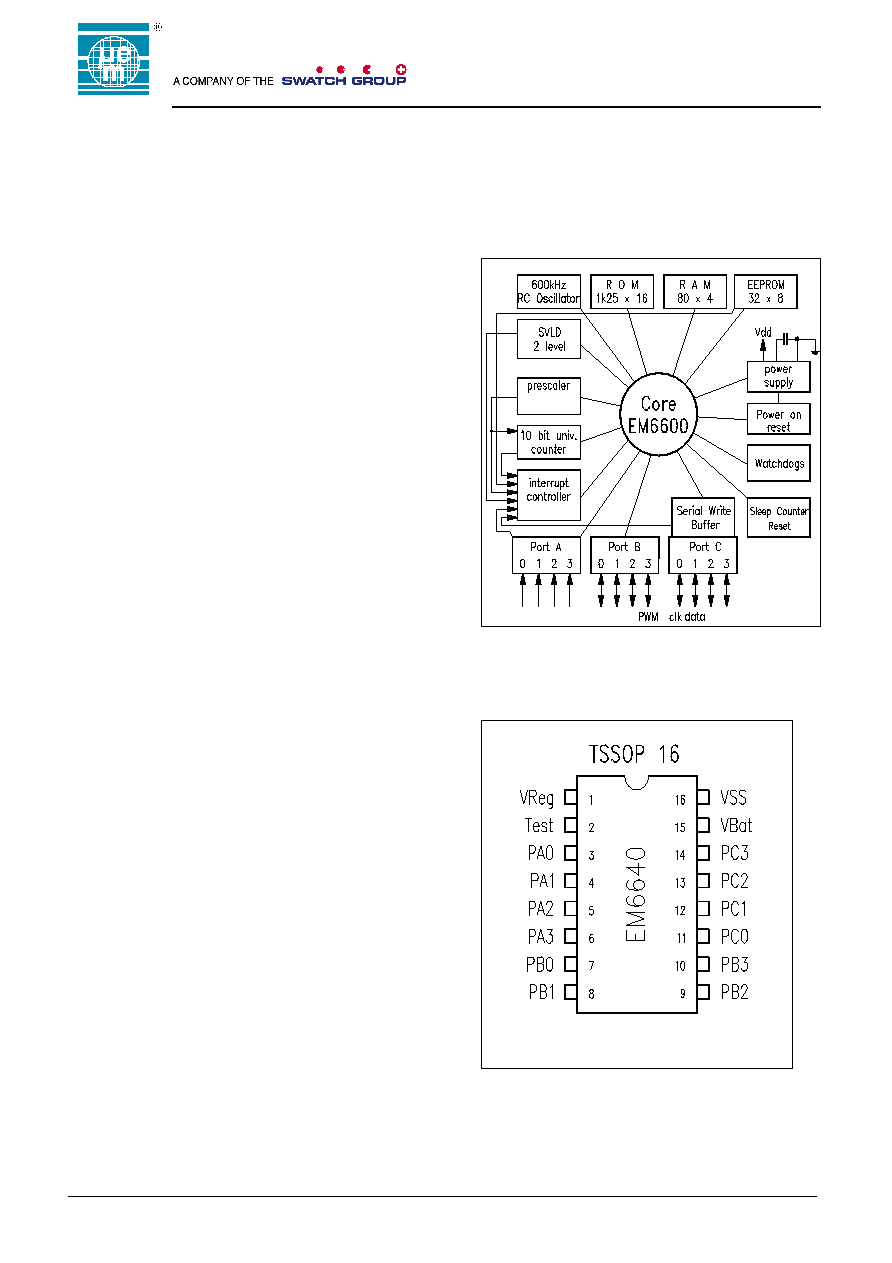
The EM6640 is an advanced single chip CMOS 4-bit
microcontroller. It contains ROM, RAM, EEPROM,
watchdog timer, oscillation detection circuit, 10 bit
up/down counter, prescaler, supply voltage level
detector (SVLD), sleep counter reset (SCR),
frequency output and SWB.
The low voltage feature and low power consumption
make it the most suitable controller for battery, stand
alone and mobile equipment. The EM66XX series is
manufactured using EM Microelectronic's Advanced
Low Power (ALP) CMOS Process.
Typical Applications
∑ remote
controls
∑ medical
applications
∑ domestic
appliance
∑ safety and security devices
∑ measurement
equipment
∑ interactive
system
∑ keyless entry with rolling code
Figure 1 Architecture
Figure 2 Pin Configuration of TSSOP16
EM MICROELECTRONIC
- MARIN SA

EM6640
03/02 REV. C/446
Copyright
2002, EM Microelectronic-Marin SA
2
www.emmicroelectronic.com
EM6640 at a glance
∑ Power Supply
- Low voltage, low power architecture
including internal voltage regulator.
- 1.9V ... 5.5V battery voltage.
- 600 kHz RC oscillator.
- 42µA typical in active mode @ 3V, 25C
∞.
- 8µA typical in standby mode @ 3V, 25C
∞.
- 0.3µA typical in sleep mode @ 3V, 25C
∞.
∑ RAM
- 80 x 4 bit, directly addressable.
∑ ROM
- 1280 x 16 bit metal mask programmable.
∑ EEPROM
- 32 x 8 bit, indirectly addressable (6 bits used to
adjust the oscillator frequency).
- Interrupt request at the end of writing operation.
- 60µA typical during read mode @ 3V, 25C
∞.
- 45µA typical during erase/write mode @ 3V, 25C
∞
∑ CPU
- 4 bits RISC architecture.
- 2 clock cycles per instruction.
- 72 basics instructions.
∑ Main Operating Modes and Resets
- Active mode (CPU is running).
- Standby mode (CPU in halt).
- Sleep mode (No clock, reset state).
- Initial reset on power on (POR).
- Watchdog timer (time out) reset.
- Oscillation detection watchdog reset.
- Reset with input combination.
∑ 4 Bits Input Port A
- Direct input read.
- Reset with input combination (register selectable).
- Debounced or direct input (register selectable).
- Interrupt request on input's rising or falling
edge (register selectable).
- Pull-up, pull-down or none (register selectable).
- Software test variables for conditional jumps.
- PA[0] and PA[3] are input for the event counter.
∑ 4 Bits Input/Output Port B
- Input or Output port bitwise.
- Direct input read.
- CMOS or N-channel open drain outputs.
- Pull-up selectable in N-channel open drain mode.
- Pull-down or pull-up selectable by register.
- Selectable pulse width modulation (PWM).
- PWM output on PB[3].
- Output frequencies 600kHz, 37.5kHz, 2.3kHz.
∑ 4 Bits Input/Output Port C
- Input or output port bitwise.
- Direct input read.
- CMOS or N-channel open drain outputs.
- Pull-up selectable in N-channel open drain mode.
- Pull-down or pull-up selectable by register.
- Serial Write Buffer clock and data output.
∑ Oscillator
- RC Oscillator at f=600kHz
±1% typ (-30∞C...40∞C).
- Absolute frequency adjustable with 6 bits EEPROM.
- No external components are necessary.
∑ Serial Write Buffer (SWB)
- Max. 256 bits long clocked with 150kHz; 75kHz
9.4kHz; 2,3kHz. External clock capability in
automatic mode, max: 1.5MHz.
- Automatic send mode: number of clocks of the last
nibble selectable by register and last data level
latched. External clock division capability by 1/1, 1/4,
1/88 and 1/352.
- Interactive send mode: interrupt request when buffer
is empty.
- Data sent at VDD or VregLogic levels selectable by
mask option.
∑ Prescaler
- 19 stages system clock divider down to 1Hz.
- 3 interrupts requests: 9.4kHz; 586Hz and 1Hz.
- Prescaler reset.
∑ Supply voltage Level Detector
- 2 levels software selectable (2,2V or 2,5V).
- Busy flag during measurement.
- Interrupt request when measurement is ready.
∑ 10-Bit Universal Counter
- 10, 8, 6, 4 bit up/down counting.
- 8 different input clocks.
- Event counting with PA[0] and PA[3] as input clocks.
- Full 10 bits or limited (8, 6, 4 bits) compare function.
- 2 interrupt requests (on compare and on 0).
- Pulse width modulation (PWM) output on PB[3].
∑ Sleep Counter Reset (SCR)
- Wake up automatically the EM6640 from sleep.
- 8 timings selectable by register.
- Inhibit SCR by register.
∑ Watchdogs
- Oscillation detection circuit.
- Digital watchdog timer reset.
∑ Interrupt Controller
- 4 external interrupt sources from PortA.
- 5 internal interrupt sources: Prescaler (3),
Timer (2), SVLD (1), EEPROM (1), SWB (1)
NB: All frequencies written in this document are related to a typical system clock of 600 kHz.

EM6640
03/02 REV. C/446
Copyright
2002, EM Microelectronic-Marin SA
3
www.emmicroelectronic.com
INDEX
FEATURES
1
1.
PIN DESCRIPTION FOR EM6640 :
3
2.
OPERATING MODES
4
2.1
ACTIVE Mode
5
2.2
STANDBY Mode
5
2.3
SLEEP Mode
5
3.
POWER SUPPLY
5
4.
RESET
6
4.1
Power-Up
7
4.2
Oscillation Detection Circuit
8
4.3
Input-PortA-Reset
9
4.4
Sleep Counter Reset (SCR)
10
4.5
Digital Watchdog Timer Reset
11
4.6
CPU State after Reset
12
5.
OSCILLATOR AND PRESCALER
13
5.1
Oscillator
13
5.2
Prescaler
14
6.
INPUT AND OUTPUT PORTS
15
6.1
Ports overview
15
6.2
PortA
16
6.2.1
IRQ on portA
16
6.2.2
Pull-up/down
17
6.2.3
Software test variables
17
6.2.4
PortA for 10-bit Counter
17
6.2.5
PortA for serial write buffer (SWB)
17
6.3
PortA registers
17
6.4
PortB
19
6.4.1
Input / Output Mode
19
6.4.2
Pull-up/Down
19
6.4.3
CMOS / Nchannel Open Drain Output
20
6.4.4
PWM and Frequency output
20
6.5
PortB registers
21
6.6
PortC
22
6.6.1
Input / Output Mode
22
6.6.2
Pull-up/Down
22
6.6.3
CMOS / Nchannel Open Drain Output
23
6.6.4
Serial Write Buffer (SWB)
23
6.7
PortC registers
23
7.
10-BIT COUNTER
24
7.1
Full, Limited Bit Counting
24
7.2
Frequency Select and Up/Down Counting
25
7.3
Event Counting
26
7.4
Compare Function
26
7.5
Pulse Width Modulation (PWM) Generation 26
7.5.1
How the PWM generator works.
27
7.5.2
PWM characteristics
27
7.6
Counter setup
27
7.7
10-bit Counter Registers
28
8.
SERIAL (OUTPUT) WRITE BUFFER - SWB
30
8.1
SWB Automatic send mode
31
8.1.1
SWB Automatic with external clock
31
8.1.2
How the SWB in automatic mode works
32
8.2
SWB Interactive send mode
33
8.2.1
How the SWB in interactive mode works
33
8.3
SWB registers
34
9.
EEPROM
36
9.1
EEPROM registers
37
10.
INTERRUPT CONTROLLER
38
10.1
Interrupt control registers
39
11.
SUPPLY VOLTAGE LEVEL DETECTOR
40
11.1
Supply Voltage Level Detector Register
40
12.
RAM
41
12.1
RAM Extension
41
13.
PERIPHERAL MEMORY MAP
42
14.
OPTION REGISTER MEMORY MAP
45
15.
TEST AT EM - ACTIVE SUPPLY CURRENT TEST 46
16.
MASK OPTIONS
47
16.1
Input / Output ports
47
16.1.1
PortA Metal Options
47
16.1.2
PortB Metal Options
48
16.1.3
PortC Metal Options
49
16.2
Digital Watchdog Option
50
16.3
SWBdataLevel Option
50
16.4
Remaining metal mask options
50
16.5
Metal mask ordering
50
17.
TEMPERATURE AND VOLTAGE BEHAVIORS
51
17.1
RC oscillator (typical)
51
17.2
IDD Current (typical)
51
17.3
Regulated Voltage (typical)
52
17.4
Output Currents (typical)
52
17.5
Pull-up/down (typical)
54
18.
EM6640 ELECTRICAL SPECIFICATIONS
55
18.1
Absolute maximum ratings
55
18.2
Handling Procedures
55
18.3
Standard Operating Conditions
55
18.4
DC characteristics - Power Supply Pins
55
18.5
Supply Voltage Level Detector
56
18.6
Oscillator
56
18.7
Analogue filter on PortA
56
18.8
Sleep counter reset (SCR)
56
18.9
EEPROM
56
18.10
DC characteristics - input / output Pins
57
18.11
DC characteristics - pull up/down
58
19.
PAD LOCATION DIAGRAM
59
20.
PACKAGE & ORDERING INFORMATION
59
20.1
Ordering Information
61
20.2
Package Marking
61
20.3
Customer Marking
61
21.
UPDATES OF SPECIFICATIONS
62
1. Pin Description for EM6640 :
Pin Number Pin Name
Function
Remarks
1
VReg
Internal voltage regulator
MFP programming connection

EM6640
03/02 REV. C/446
Copyright
2002, EM Microelectronic-Marin SA
4
www.emmicroelectronic.com
2
Test
Input test terminal
For EM test purpose only, GND 0 !
And MFP programming connection
3
Port A[0]
Input port A[0]
testvar1, event counter input, IRQPA[0],
SWB input clock
4
Port A[1]
Input port A[1]
testvar2, IRQPA[1]
5
Port A[2]
Input port A[2]
IRQPA[2]
6
Port A[3]
Input port A[3]
event counter input, IRQPA[3]
7
Port B[0]
Input/Output bitwise,
cmos/open drain port B[0]
ck[20] output
8
Port B[1]
Input/Output bitwise,
cmos/open drain port B[1]
ck[16] output
9
Port B[2]
Input/Output bitwise,
cmos/open drain port B[2]
ck[12] output
10
Port B[3]
Input/Output bitwise,
cmos/open drain port B[3]
PWM output
11
Port C[0]
Input/Output bitwise,
cmos/open drain port C[0]
SWB Clock Out
12
Port C[1]
Input/Output bitwise,
cmos/open drain port C[1]
SWB Data Out
13
Port C[2]
Input/Output bitwise,
cmos/open drain port C[2]
14
Port C[3]
Input/Output bitwise,
cmos/open drain port C[3]
15
VBat
Positive power supply terminal
VBat=VDD, MFP programming
connection
16
VSS
Negative power supply terminal reference terminal, MFP programming
connection
Figure 3 Typical configuration
C1
+
CVreg
VReg
VSS
Test
VBat
PortA
PortB
PortC
EM6640
2. Operating modes
The EM6640 has two low power dissipation modes, STANDBY and SLEEP. Figure 4 is a transition diagram for
these modes.

EM6640
03/02 REV. C/446
Copyright
2002, EM Microelectronic-Marin SA
5
www.emmicroelectronic.com
2.1 ACTIVE Mode
The active mode is the actual CPU running mode. Instructions are read from the internal ROM and executed by
the CPU. Go into standby mode via the halt instruction or go into sleep mode by writing the sleep bit.
2.2 STANDBY Mode
Executing a HALT instruction puts the EM6640 into
STANDBY mode. The voltage regulator, oscillator,
watchdog timer, interrupts and timers/counters are
operating. However, the CPU stops since the clock
related to instruction execution stops. Registers,
RAM and I/O pins retain their states prior to
STANDBY mode. STANDBY is canceled by a
RESET or an Interrupt request if enabled.
2.3 SLEEP Mode
Writing the Sleep bit in the RegSysCntl1 register
puts the EM6640 in SLEEP mode. The oscillator
stops and most functions of the EM6640 are
inactive. To be able to write the Sleep bit, the
SleepEn bit in RegSysCntl2 must first be set to "1".
In SLEEP mode only the voltage regulator is active.
The RAM data integrity is maintained. SLEEP mode
may be canceled only by the Input Reset from PortA
or the Sleep Counter Reset
.
During SLEEP mode and the following start up the EM6640 is in reset state. Waking up from SLEEP mode clears
the Sleep flag but not the SleepEn bit. Inspecting the SleepEn allows to determine if the EM6640 was powered
up (SleepEn = "0") or woken up from SLEEP mode (SleepEn = "1").
The bit NoInputRes in option register OptPaRst is inhibited is sleep mode.
TAKE CARE !!! To quit SLEEP mode, one must be sure to have a suitable defined combination of PortA inputs
for reset (see section 4.3).
Table 2.3.1 shows the state of the EM6640 functions in STANDBY and SLEEP modes
FUNCTION
STANDBY
SLEEP
Oscillator
Active
Stopped
Oscillator Watchdog
Active
Stopped
Instruction Execution
Stopped
Stopped
Interrupt Functions
Active
Stopped
Registers and Flags
Retained
Reset
EEPROM
Retained
Retained
RAM data
Retained
Retained
Option Registers
Retained
Retained
Timer/Counter's
Active
Reset
Logic Watchdog
Active
Reset
Input PortA
Active
NoInputRes = "0"
Active
NoInputRes = "x"
I/O Port B
Active
High Impedance, no pulls
I/O Port C
Active
High Impedance, no pulls
SCR
Stopped
Active if enable
SWB
Active
Stopped
Voltage Level Detector
finishes on going measure, then stop
Stopped
3. Power Supply
The EM6640 is supplied by a single external power supply between VDD (VBat) and VSS (GND). A built-in
voltage regulator generates VregLogic providing regulated voltage for the oscillator and the internal logic. An
external capacitor (CVreg) has to be put on Vreg terminal (see Standard Operating Conditions, on page 55).
Vreg terminal is not intended to be used with external load except CVreg.
Figure 4 Mode transition diagram
ACTIVE
HALT
Instruction
SLEEP bit
write
IRQ
STANDBY
SLEEP
RESET=1
RESET=0
RESET=1
RESET=1
RESET