Copyright
©
2005, EM Microelectronic-Marin SA
1
www.emmicroelectronic.com
Theseus
TM
Gold 30
EMTG30
EM MICROELECTRONIC -
MARIN SA
30KB Ultra Low Cost Flash Smart Card IC
Environment
Voltage Supply Class A, B: 3.0V to 5.0V
±
10%
-25 to +85 ∞C Operating Temperature
Max supply current 6mA @ 15MHz, Class B
> 4 kV ESD Protection HBM
CPU
Software compatible CMOS 80X51 industry standard
Accelerated architecture with 16 bit CPU performance level
Up to 30 MHz internal CPU clock
Idle Modes
Idle and Stop mode selectable modes
NVM update operation with CPU in idle/halt mode
IO Transmission and Reception with CPU in idle mode
Max Idle current / Clock stopped : 100 uA
Security
Unique chip identification number
Notification of tampering
Internal clock generation
IC operates under regulated voltage
DPA/SPA resistance mechanisms
Under / Over voltage sensors (Vcc)
Memory Control
General Purpose Non Volatile Memory: GPNVM
Secure Memory Management Mechanism
Fast Byte program: 40 us / Byte
GP NVM Page Erase: 2 ms
I/O
ISO 7816-3 compliant electrical interface
ISO 7816-3 compliant interface with T=0 and T=1 protocols
ETU Timer/Counter replacing 8051 T0/T1 Timers
Memories
768 bytes RAM (256B Local RAM + 512B XRAM)
30KB GPNVM (User) = 240 Pages of 128 B
User Code, constant storage (ROM)
User Non Volatile Data storage (EEPROM)
1KB GPNVM (System) = 8 Pages of 128 B
System parameters
Loader
extensions
Backup buffer / hard API code
10 years data retention
GPNVM Cycling Endurance > 100 K cycles
BootROM loader T0 and T14 compatible
Boot loader commands set extension capabilities
Chip Forms
8" Wafer sawn or unsawn
Back grinding and distressing options
180 microns max thickness
Modules
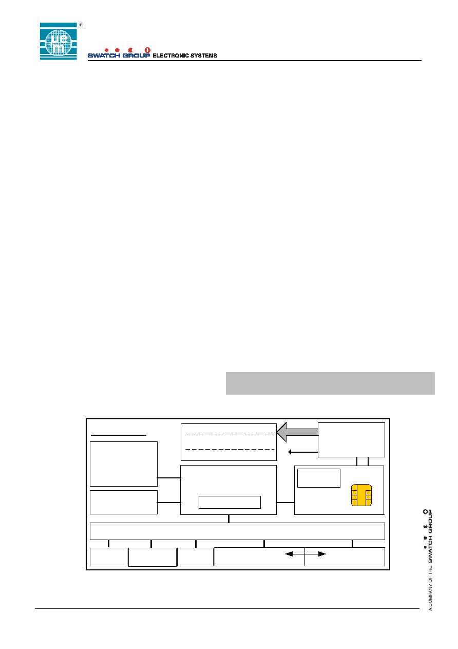
Typical Application:
SIM card GSM Phase2 or Phase2+ 16KB
A, B on-chip
Voltage Regulator
ISO 7816-3
Interface 3G
512 Bytes
RAM
SECURITY MODULE
UVD / OVD
DPA / SPA
protections
Random Number
Generator
256 Bytes RAM
Fast Architecture
80X51 Core
Internal V
DD
Power-on Reset
Power Management System
30MHz on-chip Oscillator
Controlled Clock Divider
Boot ROM
Loader
30K Bytes
GPNVM User
[ code]
[ data ]
Flexible code / data memory allocation
Secure Memory Management
EMTG30
GPNVM
System (1KB)
ETU Timer
Development tools fully integrated within Keil uVision2/3
DevKit emulator, examples, documentation samples

Copyright
©
2005, EM Microelectronic-Marin SA
2
www.emmicroelectronic.com
Theseus
TM
Gold 30
EMTG30
EM MICROELECTRONIC -
MARIN SA
Introduction
EMTG30 is a member of the Theseus family of devices
designed specifically for smart card applications. It is
software compatible with the industry standard 8051
micro-controller, to guarantee the maximum availability
of qualified software. The hardware implementation of
the core is a modern design not relying on microcode,
with an increase of up to 4 times on a standard 8051's
clocks per instruction.
Security of the family of devices makes them particularly
suitable in electronic commerce and sensitive data
areas. This is accomplished in hardware, with not only
protection against out of parameter operation of the
device, but hardware memory management to protect
against software security attacks. The CPU clock is
derived from its own internal oscillator, so preventing
attacks by clock manipulation, or extrapolating program
execution by monitoring current variations on clock
edges.
General Purpose Non Volatile Memory (GPNVM)
The General Purpose Non Volatile Memory offers ultra
low cost implementation of traditional EEPROM based
smart card ICs using one unique memory instance for
code and data storage. This one memory solution
provides compact implementation offering at the same
time a maximum flexibility. Therefore all code size
footprint reduction will directly benefits to the application.
A simple and secure memory protection mechanism is
relying on a flexible border between code and data
space.
With up to a 30KB GPNVM on chip memories EMTG30
eradicates the need for memory bank switching either
for data and code space.
The organisation of GPNVM in 128 bytes per pages
combined with efficient page management methods are
increasing application level performances such as:
-
High performances memory update
-
High resistance to page tearing
-
Extension of application level effective page cycling
endurance
-
Simple implementation of anti-tearing mechanism
An additional GPNVM system area of 1KB is available.
This system area hosts device systems parameters.
The remaining area could be used for several purposes
such boot loader commands extension, GPNVM update
backup buffer, hardware API functions etc...
This means that reel User's available memory is actually
larger than 30KB.
Serial interface
EMTG30 offers a unique serial interface compliant with
the ISO 7816-3 specification with several modes
implemented allowing serial connections at 9600 up to
357K bits per second at 3.57MHz. EMTG30 supports
T=0 asynchronous half duplex character transmission
protocol, T=1 asynchronous half duplex block
transmission and a proprietary T=14 protocol used for
fast loading of Code into the OTP by the card
manufacturer. It handles minimum guard time
requirements between characters specified by ISO7816-
3 specification automatically. EMTG30 is designed to be
compatible with the ISO7816-3 specification defining the
characteristics of Integrated Circuit Cards commonly
referred to as smart cards.
Random Number Generator
The on chip random number generator is fully Fips140-2
compliant, providing a rapid stream of truly random
numbers. This allows use of the random numbers
generated beyond just the provision of numbers for
randomising transmissions or generating keys.
Clocks
EMTG30 has its own internal oscillator this allows the
core of the device to be independent of the external
clock. The processor can also be clocked much faster
than the IO CLK signal. This ensures the elimination of
fraudulent attacks involving frequency jitter and unequal
mark space ratios. The internal clock generator is
connected to the core via a divider that is under the
control of the software. This allows the Operating
System writer to control the trade off between execution
speed and power drawn by the device. Extending
battery life in hand help applications where slow
interfaces are involved.
Anti tampering
The EMTG30 has extensive anti tampering provision
including the monitoring of the connection to the device
to ensure that deviations beyond a prescribed criteria
result in the device being closed down before its
operating conditions are violated.
On chip voltage regulators
Several on chip regulators isolate the various elements
of the device from variations and fluctuations in the
supply voltage. This allows elements to be characterised
precisely, as they operate at one fixed voltage, which in
turn maximises the endurance of the device.
Technology
This product is using superior Flash memory SuperFlash
Technology licensed from SST and SuperFlash is a
registered trademark of SST (Silicon Storage
Technology Inc.).

Copyright
©
2005, EM Microelectronic-Marin SA
3
www.emmicroelectronic.com
Theseus
TM
Gold 30
EMTG30
EM MICROELECTRONIC -
MARIN SA
Technical Data
Absolute Maximum Ratings
Parameter Symbol
Limit
Values
Unit
min typical max
Supply Operating Volt
V
cc
-0.3
6
V
Voltage at remaining pin
V
pin
V
ss
≠0.3
V
cc
+0.3 V
Power dissipation
P
tot
+60
mW
Storage temperature
I
ccI
-40
+125 ∞C
DC Characteristics
Parameter Symbol
Limit
Values
Unit
min typical max
Operating temperature
T
A
-25
+85 ∞C
Supply Voltage Class A,B
V
cc
2.7
3 / 5
5.5
V
Supply Current Class B
I
cc
6 (Note 1)
mA
Supply Current idle
I
ccI
200 (Note 2)
A
Supply Current stopped
I
ccS
100 (Note 3)
A
Note 1: The supply current refers to clock frequency of 5 Mhz
Note 2: The supply current at 3.3V and a clock frequency of 1 Mhz, at +25
0
C
Note 3: The supply current at 3.3V and +25
o
C
IO pin:
Parameter
Symbol
Conditions min max
Unit
H input voltage
V
IH
I
Ihmax
=
±
20
A
0.7 * V
cc
V
cc
V
L input voltage
V
IL
I
IL max
=
±
20
A
-0.3 0.8
V
H output voltage (Note 1)
V
OH
I
Ohmax =
+20
A
0.7 * V
cc
V
cc
V
L output voltage
V
OL
I
Olmax
= -1mA
0
0.4
V
Rise Fall Time
t
r
,
t
F
C
IN
= C
OUT
= 30 pF
1
S
NOTE 1: Assumes 20K
Pull up resistor on interface device
Clock (CLK)
Parameter Symbol
Condition
Min
Max
Unit
H output voltage
V
OH
I
Ohmax
= +20
A
V
cc
-0.7 V
cc
V
L output voltage
V
OL
I
Olmax
= -20
A
0 0.5
V
Rise Fall Time
t
r
,
t
F
C
IN
= C
OUT
= 30 pF
9% CLK
period
Reset(RST)
Parameter Symbol
Condition
Min
Max
Unit
H output voltage
V
OH
I
Ohmax
= +20
A
V
cc
-0.7 V
cc
V
L output voltage
V
OL
I
Olmax
= -20
A
0 0.6
V
Rise Fall Time
t
r
,
t
F
C
IN
= C
OUT
= 30 pF
400
s
EM Microelectronic-Marin SA (EM) makes no warranty for the use of its products, other than those expressly contained
in the Company's standard warranty which is detailed in EM's General Terms of Sale located on the Company's web
site. EM assumes no responsibility for any errors which may appear in this document, reserves the right to change
devices or specifications detailed herein at any time without notice, and does not make any commitment to update the
information contained herein. No licenses to patents or other intellectual property of EM are granted in connection with
the sale of EM products, expressly or by implications. EM's products are not authorized for use as components in life
support devices or systems.
© EM Microelectronic-Marin SA, 07/05, Rev. A/005