 | ÐлекÑÑоннÑй компоненÑ: V3020SO8B | СкаÑаÑÑ:  PDF PDF  ZIP ZIP |
Äîêóìåíòàöèÿ è îïèñàíèÿ www.docs.chipfind.ru
R
V3020
Copyright © 2005, EM Microelectronic-Marin SA
1
www.emmicroelectronic.com
Ultra Low Power 1-Bit 32 kHz RTC
Description
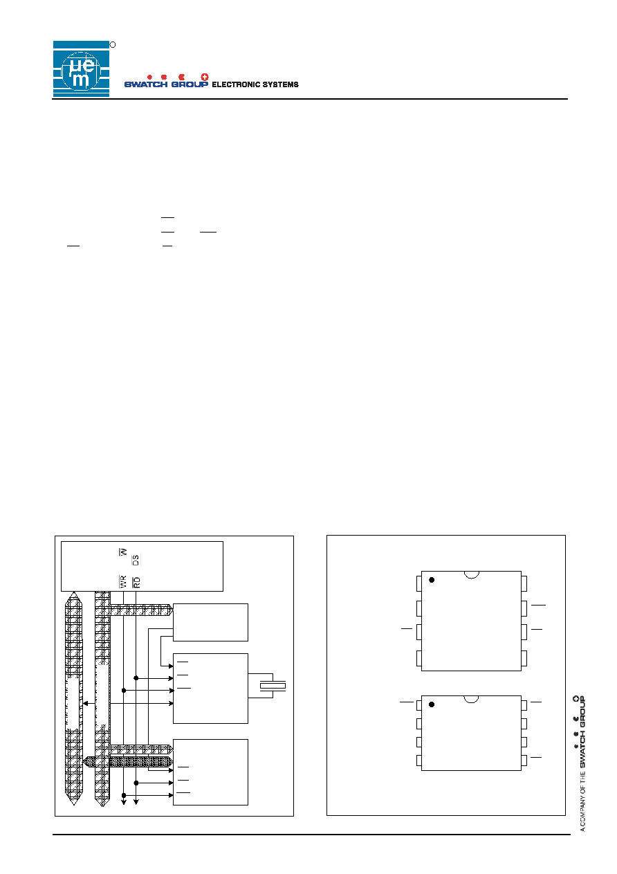
The V3020 is a low power CMOS real time clock. Data is
transmitted serially as 4 address bits and 8 data bits, over
one line of a standard parallel data bus. The device is
accessed by chip select ( CS ) with read and write control
timing provided by either
RD and WR pulse (Intel CPU)
or DS with advanced R/
W (Motorola CPU). Data can
also be transmitted over a conventional 3 wire serial
interface having CLK, data I/O and strobe. The V3020
has no busy states and there is no danger of a clock
update while accessing. Supply current is typically
390 nA at V
DD
= 3.0V. Battery operation is supported by
complete functionality down to 1.2V. The oscillator is
typically 0.3 ppm/V.
Applications
Utility meters
Battery operated and portable equipment
Consumer electronics
White/brown goods
Pay phones
Cash registers
Personal computers
Programmable controller systems
Data loggers
Automotive systems
Features
Supply current typically 390 nA at 3V
50 ns access time with 50 pF load capacitance
Fully operational from 1.2V to 5.5V
No busy states or danger of a clock update while
accessing
Serial communication on one line of a standard
parallel data bus or over a conventional 3 wire serial
interface
Interface compatible with both Intel and Motorola
Seconds, minutes, hours, day of month, month, year,
week day and week number in BCD format
Leap year and week number correction
Time set lock mode to prevent unauthorized setting of
the current time or date
Oscillator stability 0.3 ppm / volt
No external capacitor needed
Frequency measurement and test modes
Temperature range: -40°C to +85°C
On request extended temperature range, -40°C to
+125°C
Pin compatible with the V3021
TSSO8 and SO8 packages
Typical Operating Configuration
Address
Decoder
V3020
RAM
XI
XO
CS
RD
WR
I/O
CS
RD
WR
Dat
a
Bu
s
CPU
or
or R/
Ad
dr
ess
B
u
s
Fig.
1
Pin Assignment
CS
RD
WR
V
DD
I/O
V
SS
XI
XO
V3020
CS
RD
WR
V
DD
I/O
V
SS
XI
XO
V3020
SO8
TSSO8
Fig. 2
EM MICROELECTRONIC -
MARIN SA
R
V3020
Copyright © 2005, EM Microelectronic-Marin SA
2
www.emmicroelectronic.com
Absolute Maximum Ratings
Parameter Symbol
Conditions
Maximum voltage at V
DD
V
DDmax
V
SS
+ 7.0V
Minimun voltage at V
DD
V
DDmin
V
SS
0.3V
Maximum voltage at any
signal pin
V
max
V
DD
+ 0.3V
Minimum voltage at any signal
pin
V
min
V
SS
0.3V
Maximum storage
temperature
T
STOmax
+150°C
Minimum storage temperature
T
STOmin
-65°C
Electrostatic discharge
maximum to MIL-STD-883C
method 3015.7 with ref. to V
SS
V
Smax
1000V
Maximum soldering conditions
T
Smax
250°C x 10s
Table 1
Stresses above these listed maximum ratings may cause
permanent damages to the device. Exposure beyond
specified operating conditions may affect device reliability
or cause malfunction.
Handling Procedures
This device has built-in protection against high static
voltages or electric fields; however, anti-static precautions
must be taken as for any other CMOS component. Unless
otherwise specified, proper operation can only occur when
all terminal voltages are kept within the voltage range.
Unused inputs must always be tied to a defined logic
voltage level.
Operating Conditions
Parameter
Symbol
Min Typ Max
Unit
Operating temperature
1)
T
A
-40 +125
°C
Logic supply voltage
V
DD
1.2 5.0 5.5 V
Supply voltage dv/dt
(power-up & power-down)
6
V/µs
Decoupling capacitor
100
nF
Crystal Characteristics
Frequency
2)
f
32.768
kHz
Load capacitance
C
L
7 8.2
12.5
pF
Series resistance
R
S
35 50
k
Table 2
1)
The maximum operating temperature is confirmed by
sampling at initial device qualification. In production,
all devices are tested at +85°C. On request, devices
tested at +125°C can be supplied.
2)
See Fig. 5
Electrical Characteristics (standard temperature range)
V
DD
= 5.0V ±10%, V
SS
= 0V and T
A
=-40 to +85°C, unless otherwise specified
Parameter Symbol
Test
Conditions Min
Typ
Max
Unit
Total static supply
I
SS
All outputs open, all inputs at V
DD
V
DD
= 3.0V, address 0 = 0
T
A
= 0 to +°70°C
390
600
490
nA
nA
Total static supply
I
SS
All outputs open, all inputs at V
DD
V
DD
= 5V, address 0 = 0
T
A
= 0 to +°70°C
460
800
600
nA
nA
Dynamic current
I
SS
I/O to V
SS
through 1M
RD = V
SS
,
WR = V
DD
,
CS = 4 MHz
address 0 = 0, read all 0
300
µA
Input / Output
Input logic low
V
IL
1.0 V
Input logic high
V
IH
3.5
V
Output logic low
V
OL
I
OL
= 4 mA
0.4
V
Output logic high
V
OH
I
OH
= 4 mA
2.4
V
Input leakage
I
IN
0.0 < V
IN
< 5.0V
0.1
1
µA
Output tri-state leakage on I/O
pin
I
TS
CS high, and address 0, bit 0, low
0.1 1 µA
Oscillator
Starting voltage
V
STA
1.2
V
Input capacitance on XI
C
IN
T
A
= +25°C
13
pF
Output capacitance on XO
C
OUT
T
A
= +25°C
9
pF
Start-up time
T
STA
1
s
Frequency stability
f/f
1.5 V
DD
5.5V, T
A
= +25°C
0.3
0.5
ppm/V
Frequency Measurement Mode
Current source on I/O pin
pulsed on/off @ 256 Hz
I
ONF
CS high, addr.0, bit 0, high
V
I/O
= 1V
10 25 60 µA
Table 3
R
V3020
Copyright © 2005, EM Microelectronic-Marin SA
3
www.emmicroelectronic.com
Electrical Characteristics (extended temperature range)
V
DD
= 5.0V ±10%, V
SS
= 0V and T
A
=-40 to +125°C, unless otherwise specified
Parameter Symbol
Test
Conditions Min
Typ
Max
Unit
Total static supply
I
SS
All outputs open, all inputs at V
DD
V
DD
= 3.0V, address 0 = 0
4
µA
Total static supply
I
SS
All outputs open, all inputs at V
DD
address 0 = 0
7 µA
Dynamic current
I
SS
I/O to V
SS
through 1M
RD = V
SS
,
WR = V
DD
,
CS = 4 MHz
address 0 = 0, read all 0
300
µA
Input / Output
Input logic low
V
IL
1.0 V
Input logic high
V
IH
3.5
V
Output logic low
V
OL
I
OL
= 4 mA
0.4
V
Output logic high
V
OH
I
OH
= 4 mA
2.4
V
Input leakage
I
IN
0.0 < V
IN
< 5.0V
0.1
1
µA
Output tri-state leakage on I/O
pin
I
TS
CS high, and address 0, bit 0, low
0.1 1 µA
Oscillator
Starting voltage
V
STA
1.2
V
Supply voltage dV/dt (power-
up & power-down)
+85°C
T
A
+125°C
0.006
6
V/µs
Input capacitance on XI
C
IN
T
A
= +25°C
13
pF
Output capacitance on XO
C
OUT
T
A
= +25°C
9
pF
Series resistance of the
crystal
R
S
-40°C
T
A
+85°C
90
k
Start-up time
T
STA
T
A
= +125°C
1)
10
s
Frequency stability
f/f
2.0 V
DD
5.5V, T
A
= +25°C
0.3
0.5
ppm/V
Frequency Measurement Mode
Current source on I/O pin
pulsed on/off @ 256 Hz
I
ONF
CS high, addr.0, bit 0, high
V
I/O
= 1V
8 25 60 µA
Table 4
1)
Analyses done at high temperature with crystal type Micro Crystal CX2V-02
R
V3020
Copyright © 2005, EM Microelectronic-Marin SA
4
www.emmicroelectronic.com
The V3020 will run slightly too fast, in order to allow the
user to adjust the frequency, depending on the mean
operating temperature. This is made since the crystal
adjustment can only work by lowering the frequency with
an added capacitor between XO and V
SS
. The printed
circuit capacitance has also to be taken into
consideration. The V3020 in DIL 8 package, running with
an 8.2 pF crystal at room temperature, will be adjusted to
better than ±1s/day with a 6.8 pF capacitor.
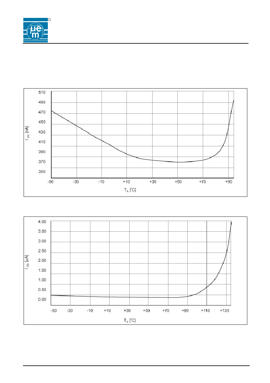
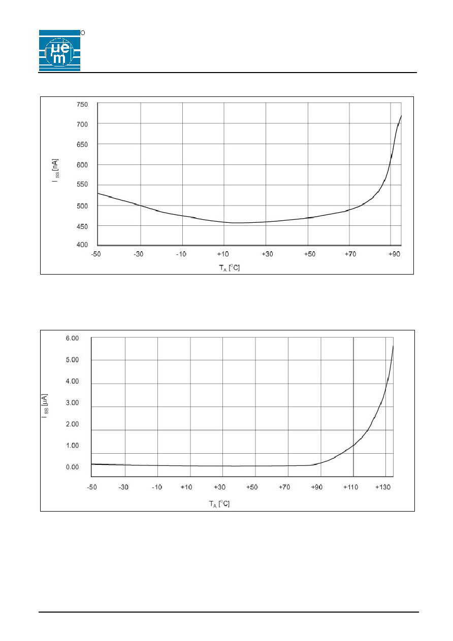
Typical Standby Current at V
DD
= 3V
Fig. 3a
Typical Standby Current at V
DD
= 3V and Extended Temperature
Fig. 3b
R
V3020
Copyright © 2005, EM Microelectronic-Marin SA
5
www.emmicroelectronic.com
Typical Standby Current at V
DD
= 5.5V
Fig. 4a
Typical Standby Current at V
DD
= 5.5V and Extended Temperature
Fig. 4b