 | –≠–ª–µ–∫—Ç—Ä–æ–Ω–Ω—ã–π –∫–æ–º–ø–æ–Ω–µ–Ω—Ç: V61188TAB | –°–∫–∞—á–∞—Ç—å:  PDF PDF  ZIP ZIP |

Features
n
n
n
n
n
n
n
n
n
n
n
n
n
n
n
n
n
n
n
n
V 6118 2 is 2 way multiplex with 2 rows and 38 columns
V 6118 4 is 4 way multiplex with 4 rows and 36 columns
V 6118 8 is 8 way multiplex with 8 rows and 32 columns
Low dynamic current, 150 A max.
Low standby current, 1 A max. at 25 C
Voltage bias and mux signal generation on chip
Display refresh on chip, 40 x 8 RAM for display storage
Display RAM addressable as 8, 40 bit words
Column driver only mode to have 40 column outputs
Separate logic and LCD supply voltage pins
Wide power supply range, V : 2 to 6 V, V
: 2 to 8 V
BLANK function for LCD blanking on power up etc.
Voltage bias inputs for applications with large pixel sizes
Bit mapped
Serial input / output
Very low external component count
-40 C to +85 C temperature range
No busy states
LCD updating synchronized to the LCD refresh signal
QFP52 and TAB packages
µ
µ
o
o
o
n
Crossfree cascadable for large LCD applications
DD
LCD
Description
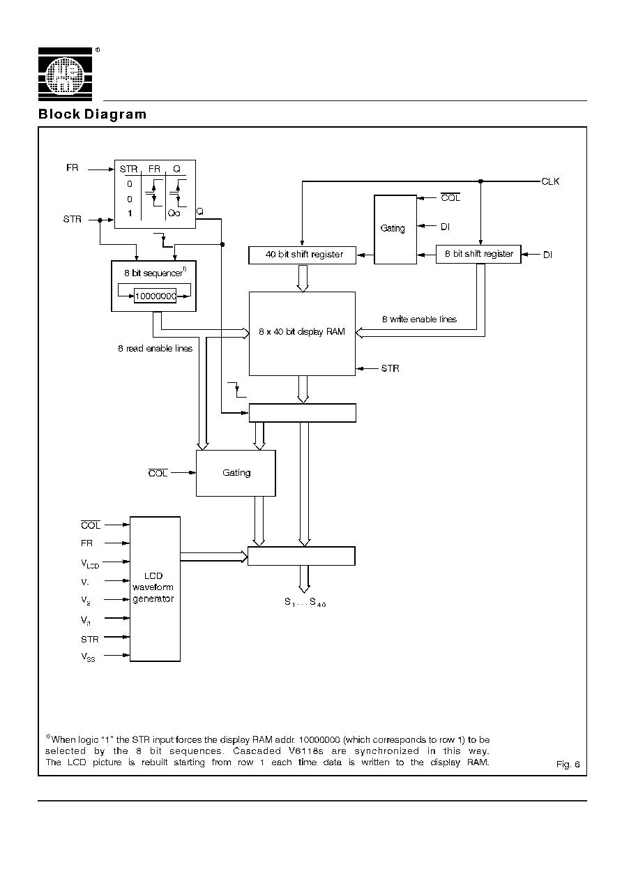
The V 6118 is a universal low multiplex LCD driver. The Ver-
sion V 6118 2 drives two ways multiplex (two blackplanes)
LCD, the version V 6118 4, four way multiplex LCD, and the
V 6118 8, eight way multiplex LCD. The display refresh is
handled on chip via a 40 x 8 bit RAM which holds the LCD
content driven by the driver. LCD pixels (or segments) are
addressed on a one to one basis with the 40 x 8 bit RAM ( a
set bit corresponds to an activated LCD pixel). The V 6118
has very low dynamic current consumption, 150 A max.,
making it particularly attractive for portable and battery
powered applications. The wide operating range on both
the logic (V ) and the LCD (V
) supply voltages offers
much application flexibility.
The LCD bias generation is
internal. The voltage bias levels can also be provided extern-
nally for applications having large pixels sizes. The V 6118
can be used as a column only driver for cascading in large
display applications. In the column only mode, 40 column
Outputs available to address the display. A BLANK func-
tion is provided to blank the LCD, useful at power up to hold
the display blank until the microprocessor has updated the
display RAM.
µ
DD
LCD
Applications
n
n
n
n
n
n
n
Balances and scales
Automotive displays
Utility meters
Large displays (public information panels etc.)
Pagers
Portable, battery operated products
Telephones
2, 4 and 8 Multiplex LCD Driver
1
Typical Operating Configuration
V6118
QFP52
V6118 8
EM MICROELECTRONIC-MARIN SA
V6118

2
Stresses above these listed maximum ratings may cause
permanent damage to the device. Exposure beyond specified
operating conditions may affect device reliability or cause
malfunction.
Absolute Maximum Ratings
V
V
V
V
T
P
V
T
DD
LCD
LOGIC
DISP
STO
MAX
SMAX
S
-0.3V to +8V
-0.3V to +9V
-0.3V to V +0.3V
DD
-0.3V to V
+0.3V
LCD
- 65 to +150 C
o
100 mW
1000V
250 C x 10 s
o
Handling Procedures
This device has built-in protection against high static voltages
or electric fields; however, anti-static precautions must be taken
as for any other CMOS component. Unless otherwise specified,
proper operation can only occur when all terminal voltages are
kept within the supply voltage range. Unused inputs must
always be tied to a defined logic voltage level.
Operating Conditions
Electrical Characteristics
I
LCD
I
DD
I
DD
I
DD
I
SS
I
IN
C
IN
V
IL
V
IH
V
IH
V
OH
V
OL
R
OUT
R
OUT
R
OUT
R
BIAS
R
BIAS
R
BIAS
±V
DC
See note
1)
See note at T = + 25 C
1)
o
A
See note
1)
See note
2)
See note at T = + 25 C
3)
o
A
0 < V < V
IN
DD
at T = + 25 C
A
o
I = 4 mA
H
I = 4 mA
L
I
= 10 A, V
= 7 V
OUT
LCD
µ
I
= 10 A, V
= 3 V
OUT
LCD
µ
I
= 10 A, V
= 2 V
OUT
LCD
µ
I
= 10 A, V
= 7 V
OUT
LCD
µ
I
= 10 A, V
= 3 V
OUT
LCD
µ
I
= 10 A, V
= 2 V
OUT
LCD
µ
See tables 4a and 4b,
V
= 5 V
LCD
0
2.0
3.0
2.4
100
0.1
3
200
0.1
1
8
0.5
1.2
9
16
18
30
30
150
1
12
250
1
100
0.8
V
DD
V
DD
0.4
1.5
2.5
20
25
50
µA
µA
µA
µA
µA
nA
pF
V
V
V
V
V
k
k
k
k
k
k
mV
1)
2)
3)
4)
5)
All outputs open, STR at V , FR = 400 Hz, all other inputs at V .
Table 3
All outputs open, STR at V , FR = 400 Hz, f
= 1 MHz, all other inputs at V .
All outputs open, all inputs at V .
This is the impedance between the voltage bias level pins (V1, V2, or V3) and the output pins S1 to S40
when a given voltage bias level is driving the outputs (S1 to S40).
This is the impedance seen at the segment pin. Outputs measured one at a time.
SS
DD
SS
CLK
DD
DD
V6118 2/4/8

3
Column Drivers
S1 to S40
logic 1
logic 0
logic 1
| Sx* - V |
S1 to S40
logic 0
logic 0
logic 1
| V
- Sx* |
| V
- Sx* | = | Sx* - V | ± 25mV
S1 to S40
logic 1
logic 0
logic 0
| V
- Sx* |
S1 to S40
logic 0
logic 0
logic 0
| Sx* - V |
| V
- Sx* | = | Sx* - V | ± 25 mV
SS
LCD
LCD
SS
LCD
SS
LCD
SS
Row Drivers
Timing Characteristics
V
= 5.0 V ± 10%, V
= 2 to 8 V, and T = -40 to +85 C
DD
LCD
A
o
Clock high pulse width
Clock low pulse width
Clock and FR rise time
Clock and FR fall time
Data input setup time
Data input hold time
Data output propagation
STR pulse width
CLK falling to STR rising
STR falling to CLK falling
FR frequency (Vers. 2/4/8)
t
CH
t
CL
t
CR
t
CF
t
DS
t
DH
t
PD
t
STR
t
P
t
D
F
FR
2)
C
= 50 pF
LOAD
120
120
20
1)
30
1)
100
10
200
128/256/512
200
200
100
ns
ns
ns
ns
ns
ns
ns
ns
ns
ns
Hz
Clock high pulse width
Clock low pulse width
Clock and FR rise time
Clock and FR fall time
Data input setup time
Data input hold time
Data output propagation
STR pulse width
CLK falling to STR rising
STR falling to CLK falling
FR frequency (Vers. 2/4/8)
t
CH
t
CL
t
CR
t
CF
t
DS
t
DH
t
PD
t
STR
t
P
t
D
F
FR
2)
C
= 50 pF
LOAD
500
500
100
1)
150
1)
500
10
1
128/256/512
200
200
400
ns
ns
ns
ns
ns
ns
ns
ns
ns
µ
s
Hz
V6118 2/4/8

4
DI
Col39
1)
A set address bit corresponds to a write enabled RAM
address,the same data can be written to more than one
RAM address by setting the required address bits.
CLK
STR
V 6118 as a row and column driver (
inactive)
40 bit load cycle, RAM address provided by address bit 1 to (n*)
COL
1)
A set address bit corresponds to a write enabled RAM
Address, the same data can be written to more than one
RAM address by setting the required address bits.
*
n = the V6118 version number (i.e. 2,4, or 8)
DI
CLK
STR
V6118 2/4/8
5
40 bit display latch
40 display driver outputs
X
V6118 2/4/8