 | –≠–ª–µ–∫—Ç—Ä–æ–Ω–Ω—ã–π –∫–æ–º–ø–æ–Ω–µ–Ω—Ç: V6123 | –°–∫–∞—á–∞—Ç—å:  PDF PDF  ZIP ZIP |

Digitally Programmable 2, 4 and 8 Mux LCD Driver
Features
n
Very simple 1-bit interface (see Fig. 1)
n
V6123 mux mode 2 with 2 rows and 58 columns
n
V6123 mux mode 4 with 4 rows and 56 columns
n
V6123 mux mode 8 with 8 rows and 52 columns
n
Very simple 1-bit interface, reduced to its simplest
form
n
Frame frequency on chip by internal RC oscillator
n
Voltage bias and mux signal generation on chip
n
1 display RAM addressable as 8 x 60 bit words
n
Column driver only mode to have 60 column outputs
n
No busy states
n
No external components needed
n
Blank function for LCD blanking
n
Bit mapped
n
Wide V
DD
voltage supply range, 2 to 6 V
n
Wide V
LCD
voltage supply range, 2 to 8.5 V
n
-40 to + 85 ∞C temperature range
Description
The V6123 is a low mul ti plex LCD driver. The 2, 4 and 8
way mul ti plex is dig i tally pro gram ma ble by the com mand
byte. The dis play re fresh is han dled on chip by an in ter nal
RC os cil la tor via 1 selectable 8 x 60 RAM which holds the
LCD con tent driven by the driver. LCD pix els (or seg-
ments) are ad dressed on a one to one ba sis with the 8 x
60 bit RAM (a set bit cor re sponds to an ac ti vated LCD
pixel).
The V6123 has a very low dy namic cur rent con sump tion,
typ i cally 175 µA at V
DD
= 5 V, V
LCD
= 7 V, mak ing it par tic u -
larly at trac tive for por ta ble and bat tery pow ered prod ucts.
The wide op er at ing range on sup ply volt ages and tem -
per a ture of fers much ap pli ca tion flex i bil ity. The LCD bias
gen er a tion and frame fre quency are gen er ated on chip.
The clock sig nal can be used to shift and to latch the data
into the RAM.
Applications
n
Automotive displays
n
Telephones
n
Pagers
n
Portable, battery operated products
n
Large displays (public information panels, etc.)
n
Balances and scales
n
Utility meters
1
V6123
EM MICROELCTRONIC-MARIN SA
Pad Assignment
Typical Operating Conditions
Fig. 1
Fig. 2

Absolute Maximum Ratings
Parameter
Symbol
Conditions
Supply voltage range
V
DD
-0.3 V to 9 V
LCD supply voltage range
V
LCD
-0.3 V to 10 V
Voltage at DI, DO, CLK, FR
V
LOGIC
-0.3 V to V
DD
+0.3 V
Voltage at V1 to V3, S1 to S60
V
DISP
-0.3 V to V
LCD
+0.3 V
Storage temperature range
T
STO
-65 to +150 ∞C
PElectrostatic discharge max.
to MIL-STD-883C method 3015
V
Smax
1000 V
Maximum soldering conditions
T
Smax
250 ∞C x 10 s
Ta ble 1
Stresses above these listed max i mum rat ings may cause
per ma nent dam age to the de vice. Ex po sure be yond
spec i fied op er at ing con di tions may af fect de vice re li abil -
ity or cause mal func tion.
Handling Procedures
This de vice has built-in pro tec tion against high static volt -
ages or elec tric fields; how ever, anti-static pre cau tions
must be taken as for any other CMOS com po nent. Un less
oth er wise spec i fied, proper op er a tion can only oc cur
when all ter mi nal volt ages are kept within the sup ply volt -
age range. Un used in puts must al ways be tied to a de -
fined logic volt age level.
Operating Conditions
Parameter
Symbol Min. Typ. Max. Unit
Operating temperature
T
A
-40
+85 ∞C
Logic supply voltage
V
DD
2
5
6
V
LCD supply voltage
V
LCD
2
5
8.5
V
Ta ble 2
2
V6123
Electrical Characteristics
V
DD
= 5 V ± 10%, V
LCD
= 2 to 8.5 V and T
A
= -40 to +85 ∞C, un less oth er wise spec i fied
Parameter
Symbol Test Conditions
Min.
Typ.
Max.
Units
Dynamic supply current
I
LCD
See note
1)
175
250
µA
Dynamic supply current
I
DD
See note
1)
at T
A
= 25 ∞C
29
35
µA
Dynamic supply current
I
DD
See note
1)
29
50
µA
Dynamic supply current
I
DD
See note
2)
285
350
µA
Control Signals DI, CLK, FR
Input leakage
I
IN
0 < V
IN
< V
DD
1
100
nA
Input capacitance
C
IN
at T
A
= 25 ∞C
8
pF
Low level input voltage
V
IL
0
0.8
V
High level input voltage
V
IH
2.0
V
DD
V
Data Output DO
High level output voltage
V
OH
I
H
= 2 mA
2.4
V
Low level output voltage
V
OL
I
L
= 2 mA
0.4
V
Driver Outputs S1 ... S60
Driver impedance
4)
R
OUT
I
OUT
= 10 µA, V
LCD
= 7 V
1
1.5
k
Driver impedance
4)
R
OUT
I
OUT
= 10 µA, V
LCD
= 3 V
2.6
3.5
k
Driver impedance
4)
R
OUT
I
OUT
= 10 µA, V
LCD
= 2 V
7
k
Bias impedance V1, V2, V3
5)
R
BIAS
I
OUT
= 10 µA, V
LCD
= 7 V
18
24
k
Bias impedance V1, V2, V3
5)
R
BIAS
I
OUT
= 10 µA, V
LCD
= 3 V
20
27
k
Bias impedance V1, V2, V3
5)
R
BIAS
I
OUT
= 10 µA, V
LCD
= 2 V
24
k
DC output component
± VDC
see Tables 4a and 4b, V
LCD
= 5 V
15
50
mV
1)
All out puts open, DI and CLK at V
SS
, FR = 400 Hz, all other in puts at V
DD
Ta ble 3
2)
All out puts open, DI at V
SS
, FR = 400 Hz, f
CLK
= 1 MHz
3)
All out puts open, all in puts at V
DD
4)
This is the im ped ance be tween of the volt age bias level pins (V1, V2 or V3) and the out put pins S1 to S60 when a given volt age
bias level is driv ing the out puts (S1 to S60)
5)
This is the im ped ance seen at the seg ment pin. Out puts mea sured one at a time

V6123
3
Column Drivers
Outputs
FR Polarity
Column Data
Measured
Guaranteed
S1 to S60
logic 1
logic 1
| Sx* - V
SS |
S1 to S60
logic 0
logic 1
| V
LCD
- Sx* |
| V
LCD
- Sx* | = | Sx* - V
SS
| ± 25 mV
S1 to S60
logic 1
logic 0
| V
LCD
- Sx* |
S1 to S60
logic 0
logic 0
| Sx* - V
SS
|
| V
LCD
- Sx* | = | Sx* - V
SS
| ± 25 mV
*Sx = the out put num ber (I.e. S1 to S60)
Ta ble 4a
Row Drivers
Outputs
FR Polarity
Row Data
Measured
Guaranteed
S1 to Sn*
logic 1
logic 1
| V
LCD
- Sx |
S1 to Sn*
logic 0
logic 1
| Sx - V
ss |
| V
LCD
- Sx | = | Sx - V
SS
| ± 25 mV
S1 to Sn*
logic 1
logic 0
| Sx - V
SS
|
S1 to Sn*
logic 0
logic 0
| V
LCD
- Sx |
| V
LCD
- Sx | = | Sx - V
SS
| ± 25 mV
*n= the V6123 mux programme num ber (i.e. 2, 4 or 8)
Ta ble 4b
Timing Characteristics
V
DD
= 5 V ± 10%, V
LCD
= 2 to 8.5 V, and T
A
= -40 ∞C to +85 ∞C
Parameter
Symbol Test Conditions
Min.
Typ.
Max.
Units
Clock high pulse width
t
CH
120
ns
Clock low pulse width
t
CL
120
2000
ns
Clock and FR rise time
t
CR
200
ns
Clock and FR fall time
t
CF
200
ns
Data input setup time
t
DS
20
1)
ns
Data input hold time
t
DH
30
1)
ns
Data output propagation
t
PD
C
LOAD
= 50 pF
200
ns
STR pulse width
t
STR
6
µs
FR (internal frame frequency)
f
FR
2)
T
A
= 25 ∞C
45
55
65
Hz
1)
t
DS
+ t
DH
min i mum must be
100 ns. If t
DS
= 20 ns then t
DH
80 ns.
Ta ble 5a
2)
V6123 n, FR = n times the de sired LCD re fresh rate where n is the V6123 mux mode num ber.
See fig. 14, 15 for more de tails con cern ing frame fre quency.
V
DD
= 2 to 6V, V
LCD
= 2 to 8.5 V, and T
A
= -40 ∞C to +85 ∞C
Parameter
Symbol Test Conditions
Min.
Typ.
Max.
Units
Clock high pulse width
t
CH
0.5
µs
Clock low pulse width
t
CL
0.5
1.5
µs
Clock and FR rise time
t
CR
200
ns
Clock and FR fall time
t
CF
200
ns
Data input setup time
t
DS
100
1)
NS
Data input hold time
t
DH
150
1)
ns
Data output propagation
t
PD
C
LOAD
= 50 pF
500
ns
STR pulse width
t
STR
16
µs
1)
t
DS
+ t
DH
min i mum must be
500 ns. If t
DS
= 100 ns then t
DH
400 ns.
Ta ble 5b

4
V6123
Timing Waveforms
Clock Definition
Programmation Data Bits and Data Transfer Cycle
Fig. 4
Fig. 3
Com mand Bits 0 to 7
0
1
2
3
4
5
6
7
Mul ti plex
COL
RAM Ad dress
Blank SET
Ra tio
Bit2: COL bit con fig ure the V6123 func tion as row and
col umn driver or col umn driver only.
Bit 6: Blank bit forces all col umn out puts OFF.
Bit 7: SET bit forces all col umn out puts ON.
Note: If bit 6 and 7 are both to 1L the chip is syn -
chro nized to row 1.
Mux Ra tio (bit 0, 1)
0
1
Mux Mode
0
0
2
0
1
4
1
0
-
1
1
8
V6123 as a row and col umn driver, 68 bit load cy cle,
RAM ad dress aris ing from com mand bits 3 to 5
Display RAM Address
Com mand Bits 3 to 5
Mux
Mux
Mux
LCD
prog. 2 prog. 4 prog. 8
Row
000
000
000
Row 1
001
001
001
Row 2
010
010
Row 3
011
011
Row 4
100
Row 5
101
Row 6
110
Row 7
111
Row 8
All mux mode programmation or COL states need 68
bit load cy cles.
Fig. 5

5
V6123
Block Diagram
10000000
Fig. 6

V6123
Pin Assignment
Name
Function
S1 ... S60 LCD outputs, see Table 7
V3
LCD voltage bias level 3
1) 2)
V2
LCD voltage bias level 2
1)
V1
LCD voltage bias level 1
1)
V
LCD
Power supply for the LCD
FR
AC I/O signal for LCD driver output
DI
Serial data input
DO
Serial data output
CLK
Data clock input
V
DD
Power supply for logic
V
SS
Supply GND
Ta ble 6
1)
The V6123 has in ter nal volt age bias level gen er a tion. When
driv ing large pix els, an ex ter nal re sis tor di vider chain can be
connnected to the volt age bias level in puts to ob tain en hanced
dis play con trast. See Fig. 11, 12 and 13. The ex ter nal re sis tor
di vider ra tio should be in ac cor dance with the in ter nal re sis tor
ra tio (see Ta ble 8).
2)
V3 is con nected in ter nally to V
SS
on the V6123 mux mode 4.
Name
COL in ac tive
COL ac tive
V6123 (2) V6123 (4) V6123 (8)
S1
Row1
Row1
Row1
Col1
S2
Row2
Row2
Row2
Col2
S3
Col1
Row3
Row3
Col3
S4
Col2
Row4
Row4
Col4
S5
Col3
Col1
Row5
Col5
S6
Col4
Col2
Row6
Col6
S7
Col5
Col3
Row7
Col7
S8
Col6
Col4
Row8
Col8
S9...S60 Col7...58 Col5...56 Col1...52 Col9...60
Ta ble 7
6
LCD Voltage Bias Levels
Ta ble 8
LCD Drive
Type
LCD Bias
Con fig u ra tion
V
OP
3)
V
OFF
(rms)
V
ON
(rms)
V
OFF
(rms)
3)
V
OP
= V
LCD
- V
SS

7
V6123
Row and Column Multiplexing Waveform V6123 (2)
V
OP
= V
LCD
≠ V
SS
, V
STATE
= V
COL
≠ V
ROW
* See ta ble 8
Fig. 7

8
V6123
Row and Column Multiplexing Waveform V6123 (4)
V
OP
= V
LCD
≠ V
SS
, V
STATE
= V
COL
≠ V
ROW
Fig. 8
* See ta ble 8

9
V6123
Row and Column Multiplexing Waveform V6123 (8)
V
OP
= V
LCD
≠ V
SS
, V
STATE
= V
COL
≠ V
ROW
Fig. 9
* See ta ble 8

10
V6123
Functional Description
Supply Voltage V
LCD
, V
DD
, V
SS
The volt age be tween V
DD
and V
SS
is the sup ply volt age for
the logic and the in ter face. The volt age be tween V
LCD
and
V
SS
is the sup ply volt age for the LCD and is used for the
gen er a tion of the in ter nal LCD bias level which have a
max i mum im ped ance of 30 k
for a volt age from 3 to
8.5 V. With out ex ter nal con nec tions to the V1, V2, V3 bias
level in puts, the V6123 can drive most me dium sized LCD
(pixel aera up to 4'000 mm
2
).
For dis plays with a wide vari a tion in pixel sizes, the con -
fig u ra tion shown in Fig. 12 can give en hanced con trast by
giv ing faster pixel switch ing times. On chang ing the row
po lar ity (see Fig. 7, 8 and 9) the par al lel ca pac i tors lower
the im ped ance of the bias level gen er a tion to the peak
cur rent, giv ing faster pixel charge times and thus a higher
RMS "on" value. A higher RMS "on" value can give better
con trast. If for a given LCD size and op er at ing volt age, the
"off" pix els ap pear
"on", or there is poor con trast, then an
ex ter nal bias level gen er a tion cir cuit can be used with the
V6123. An ex ter nal bias gen er a tion cir cuit can lower the
bias level im ped ance and hence im prove the LCD con -
trast (see Fig. 11). The op ti mum val ues of R, Rx and C,
vary ac cord ing to the LCD size used and V
LCD
. They are
best de ter mined through ac tual ex per i men ta tion with the
LCD.
For LCD with very large av er age pixel area (eg. up to
10'000 mm
2
), the bias level con fig u ra tion shown in Fig. 13
should be used.
When V6123 are cas caded, con nect the V1, V2 and V3
bias in puts as shown in Fig. 10. The pixel load is av er -
aged across all the cas caded driv ers. This will give en -
hanced dis play con trast as the ef fec tive bias level source
im ped ance is the par al lel com bi na tion of the to tal num -
ber of driv ers. For ex am ple, if two V6123 are cas caded as
shown in Fig. 10, then the max i mum bias level im ped -
ance be comes 15 k
for a V
LCD
volt age from 3 to 8.5 V.
Ta ble 8 shows the re la tion ship be tween V1, V2 and V3 for
the mul ti plex rates 2, 4 and 8. Note that V
LCD
> V1 > V2 >
V3 for the V6123 2 and 8 mux pro grammed, and for the
V6123 4 mux pro grammed, V
LCD
> V1 > V2, and V3 = V
SS
.
Data Input / Output
The data in put pin, DI, is used to load se rial data into the
V6123. The se rial data word length is 68 bits. Data is
loaded in in verse nu mer i cal or der, the data for bit 68 is
loaded first, the data for bit 1 last. The col umn data bits
are loaded first and then the com mand byte (see Fig. 5).
The data out put pin, DO, is used in cas caded ap pli ca tion
(see Fig. 10). DO trans fers the data to the next cas caded
chip. The data at DO is equal to the data at DI de layed by
68 clock pe ri ods. In or der to cas cade V6123s, the DO of
one chip must be con nected to DI of the fol low ing chip
(see Fig. 10).
In cas caded ap pli ca tions the data for the last V6123 (the
one that does not have DO con nected) must be loaded
first and the data for the first V6123 (it is DI con nected to
the pro ces sor) loaded last.
The dis play RAM word length is 60 bits (see Fig. 6). Each
LCD row has a cor re spond ing dis play RAM ad dress
which pro vides the col umn data (on or off) when the row
is se lected (on). When down load ing data to the V6123,
any dis play RAM ad dress can be cho sen. Dis play RAM
ad dress is given by com mand bits 3 to 5. Bit 6 forces all
col umn out puts at 0L (dis play OFF). Bit 7 forces all col -
umn out puts at 1L (dis play ON). If bit 7 (SET) and bit 6
(BLANK) are both ac tive, the ini tial iza tion func tion is ac ti -
vated. This func tion is used to syn chro nize the chip at row
one. The com mand bit 2 (COL) de fines the V6123 as a
row and col umn driver or col umn driver only. The V6123
func tions as row and col umn driver while the bit 2 (COL)
is in ac tive. When ac tive, the bit 2 configures the V6123 to
func tion as col umn driver only. The for mer row out puts
func tion as col umn out puts. In cas caded ap pli ca tions,
one V6123 should be used in the row and col umn con fig -
u ra tion (COL in ac tive) and the rest as pure col umn driv -
ers (COL ac tive) (see Fig. 10). Note when cas cad ing
V6123s never cas cade one mux mode num ber with an -
other. If a V6123 8 mux pro grammed is used to drive the
rows, then only V6123 8 mux pro grammed can be cas -
caded with it.
The com mand bits, bit 1 and bit 0, de fine the mux mode
(see Fig. 5).
CLK Input
The clock in put is used to clock the DI se rial data into the
shift reg is ter, to latch the data from the shift reg is ter into
the RAM .
Af ter load ing data into the shift reg is ter, the clock has to
stay 0 logic dur ing T
STR
.
Af ter T
STR
pulse, the data are latched into the RAM.
FR Input / Output
The frame fre quency is re al ized by an in ter nal RC os cil la -
tor with a typ i cal value of 55 Hz. The in ter nal row fre -
quency changes with the num ber of rows (F
row
= 55 x n,
where n = 2, 4 or 8).
When bit 2 (COL) is in ac tive (row and col umn driver), the
frame fre quency is given by the in ter nal os cil la tor. This
fre quency can also be used at FR out put to drive
casecaded V6123.
When bit 2 (COL) is ac tive (col umn driver only), the frame
fre quency is ex ter nal then the fre quency is given by the
row and col umn driver di rectly to the FR in put. In cas -
caded ap pli ca tions, the row and col umn driver (FR, out -
put) give the frame fre quency to all the cas caded chip
(FR, in put).
Driver Outputs S1 to S60
There are 60 LCD driver out puts on the V6123. When bit 2
(COL) is in ac tive, the out puts S1 to Sn func tion as row
driv ers and the out puts S(n+1) to S60 func tion as col umn
driv ers. Where n is the V6123 mux mode num ber (2, 4 or
8).
When bit 2 (COL) is ac tive, all 60 out puts func tion as col -
umn driv ers (see Ta ble 6). There is a one to one re la tion -
ship be tween the dis play RAM and the LCD driver

11
V6123
out puts. Each pixel (seg ment) driven by the V6123 on the
LCD has a dis play RAM bit which cor re sponds to it. Set -
ting the bit turns the seg ment "on" and clear ing it turns it "off".
Power-Up
On power up the data in the shift reg is ters, the dis play
RAM, the se quencer driv ing the 2/4/8 rows and the 60 bit
dis play latches are un de fined.
Applications
Two V6123 8 Mux Programmed Cascaded
Fig. 10
By con nect ing the V1, V2 and
V3 bias in puts as shown, the
pixel load is av er aged across
all the driv ers. The ef fec tive
bias level source im ped ance
is the par al lel com bi na tion of
the to tal num ber of driv ers.
For ex am ple, if two V6123 are
cas caded as above, then the
max i mum bias level im ped -
ance be comes 15 k
.
V6123 8 Mux Programmed with External Resistor Divider Bias Generation
Fig. 11
Ex am ple set val ues:
R = 3.3 - 10 k
C = 2.2 - 47 nF
Rx is given by the for mula:
Rx = 4R ((V
DISP
/V
LCD
)-1) = 10 - 30 k

12
V6123
Enhanced Switching from the V6123
Bias Configuration for Large LCD
C = 1 µF
Rx is given by the for mula:
Rx = 4(24 k
)
(
(V
DISP
/V
LCD
) ≠ 1
)
Large LCD ex am ple:
V
OP
= 5 V, av er age pixel ac tive area = up to
10'000 mm
2
, displasy re fresh rate = 55 Hz
For a sin gle V6123 4 mux pro grammed driv ing
such an LCD, the volt age fol lower buffer (opamp)
re quire ment is:
peak cur rent 1.8 mA
steady state cur rent typ i cally 150 µA
Fig. 13
Fig. 12
Frame Frequency vs. Temperature at V
DD
= 4.5 V
Frame Frequency vs. V
DD
at T
A
= 25∞C
Fig. 14
Fig. 15
Tem per a ture com pen sa tion/
Con trast ad just ment
13
V6123
Application Example
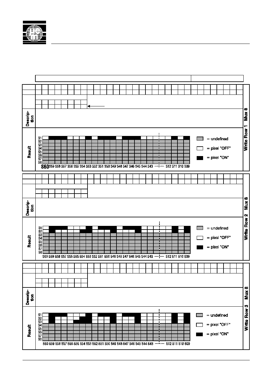
This ta ble shows how to use the V6123 with a given ini tial iza tion for Chip-on-Glas. Rows "Data" show the log i cal value
to af fect pad DI for each falling edge of pad CLK. Af ter load ing data into the shift reg is ter, the clock has to stay logic 0
dur ing t
STR
. Af ter the t
STR
pulse the data are latched into the RAM.
Display Data 8 Bits "don't care"
Bit No
67
66 65 64 63 62 61 60 59 58 57 56 55 54 53 52 51 ... ... 20 19 18 17 16 15 14 13 12 11 10 9 8
DATA 0 1 1 1 0 0 0 1 0 1 1 1 0 1 1 1 0
0 0 1 0 1 X X X X X X X X
Com mand Byte
7 6 5 4 3 2 1 0
0 0 0 0 0 1 1 1
Last send
Bit 7,6 = 0,0:
no set, no blank
Bit 3 to 5 = 0,0,0: data sent to row 1 of the RAM
Bit 2 = 1:
row and col umn driver con fig u ra tion
Bit 0,1 = 1,1:
mux 8
Fig.16.01
Bit No 67 66 65 64 63 62 61 60 59 58 57 56 55 54 53 52 51 ... ... 20 19 18 17 16 15 14 13 12 11 10 9 8
DATA 0 1 0 0 0 0 1 1 0 0 0 1 0 0 0 1 0
0 0 1 0 1 X X X X X X X X
Com mand Byte
7 6 5 4 3 2 1 0
0 0 1 0 0 1 1 1
Bit 7,6 = 0,0:
no set, no blank
Bit 3 to 5 = 0,0,1: data sent to row 2 of the RAM
Bit 2 = 1:
row and col umn driver con fig u ra tion
Bit 0,1 = 1,1:
mux 8
Fig.16.02
Bit No 67 66 65 64 63 62 61 60 59 58 57 56 55 54 53 52 51 ... ... 20 19 18 17 16 15 14 13 12 11 10 9 8
DATA 0 1 0 0 0 1 1 1 0 0 0 1 0 0 0 1 0
0 0 1 0 1 X X X X X X X X
Com mand Byte
7 6 5 4 3 2 1 0
0 0 0 1 0 1 1 1
Bit 7,6 = 0,0:
no set, no blank
Bit 3 to 5 = 0,1,0: data sent to row 3 of the RAM
Bit 2 = 1:
row and col umn driver con fig u ra tion
Bit 0,1 = 1,1:
mux 8
Ta ble 9 (con tin ued on fol low ing pages)
Fig.16.03

Ta ble 9 con tin ued
14
V6123
Bit No 67 66 65 64 63 62 61 60 59 58 57 56 55 54 53 52 51 ... ... 20 19 18 17 16 15 14 13 12 11 10 9 8
DATA 0 1 0 1 0 0 0 1 0 1 0 0 0 0 0 1 0
0 0 1 0 1 X X X X X X X X
Com mand Byte
7 6 5 4 3 2 1 0
0 0 1 0 1 1 1 1
Bit 7,6 = 0,0:
no set, no blank
Bit 3 to 5 = 1,0,1: data sent to row 6 of the RAM
Bit 2 = 1:
row and col umn driver con fig u ra tion
Bit 0,1 = 1,1:
mux 8
Fig.16.06
Display Data 8 Bits "don't care"
Bit No 67 66 65 64 63 62 61 60 59 58 57 56 55 54 53 52 51 ... ... 20 19 18 17 16 15 14 13 12 11 10 9 8
DATA 0 1 0 1 0 0 0 1 0 1 0 0 0 0 0 1 0
0 0 1 0 1 X X X X X X X X
Com mand Byte
7 6 5 4 3 2 1 0
0 0 0 0 1 1 1 1
Bit 7,6 = 0,0:
no set, no blank
Bit 3 to 5 =1,0,0:
data sent to row 5 of the RAM
Bit 2 = 1:
row and col umn driver con fig u ra tion
Bit 0,1 = 1,1:
mux 8
Fig.16.05
Bit No 67 66 65 64 63 62 61 60 59 58 57 56 55 54 53 52 51 ... ... 20 19 18 17 16 15 14 13 12 11 10 9 8
DATA 0 1 1 1 0 0 0 1 0 1 1 1 0 0 1 1 0
0 0 1 0 1 X X X X X X X X
Com mand Byte
7 6 5 4 3 2 1 0
0 0 1 1 0 1 1 1
Bit 7,6 = 0,0:
no set, no blank
Bit 3 to 5 = 0,1,1: data sent to row 4 of the RAM
Bit 2 = 1:
row and col umn driver con fig u ra tion
Bit 0,1 = 1,1:
mux 8
Fig.16.04
Ta ble 9 (con tin ued on next pages)

Table 9 continued
15
V6123
Com mand Byte
Bit No 7 6 5 4 3 2 1 0
DATA 1 0 1 1 1 1 1 1
Bit 7,6 = 1,0:
SET, no blank
Bit 3 to 5 = 1,1,1: data sent to row 8 of the RAM
Bit 2 = 1:
row and col umn driver con fig u ra tion
Bit 0,1 = 1,1:
mux 8
Fig.16.09
Display Data 8 Bits "don't care"
Bit No 67 66 65 64 63 62 61 60 59 58 57 56 55 54 53 52 51 ... ... 20 19 18 17 16 15 14 13 12 11 10 9 8
DATA 0 0 0 0 0 0 0 0 0 0 0 0 0 0 0 0 0
0 0 0 0 0 X X X X X X X X
Com mand Byte
7 6 5 4 3 2 1 0
0 0 1 1 1 1 1 1
Bit 7,6 = 0,0:
no set, no blank
Bit 3 to 5 = 1,1,1: data sent to row 8 of the RAM
Bit 2 = 1:
row and col umn driver con fig u ra tion
Bit 0,1 = 1,1:
mux 8
Fig.16.08
Bit No 67 66 65 64 63 62 61 60 59 58 57 56 55 54 53 52 51 ... ... 20 19 18 17 16 15 14 13 12 11 10 9 8
DATA 0 1 1 1 0 0 0 1 0 1 1 1 0 1 1 1 0
0 0 0 1 0 X X X X X X X X
Com mand Byte
7 6 5 4 3 2 1 0
0 0 0 1 1 1 1 1
Bit 7,6 = 0,0:
no set, no blank
Bit 3 to 5 = 1,1,0: data sent to row 7 of the RAM
Bit 2 = 1:
row and col umn driver con fig u ra tion
Bit 0,1 = 1,1:
mux 8
Fig.16.07
Ta ble 9 (con tin ued on next pages)

Table 9 continued
16
V6123
Bit No 67 66 65 64 63 62 61 60 59 58 57 56 55 54 53 52 51 ... ... 20 19 18 17 16 15 14 13 12 11 10 9 8
DATA 0 0 0 0 0 0 0 0 0 0 0 0 0 0 0 0 0
0 0 0 0 0 X X X X X X X X
Com mand Byte
7 6 5 4 3 2 1 0
1
1 1 1 1 1 1 1
Bit 7,6 = 1,1:
no set, no blank
Syn chro nize the chip at row 1
Bit 3 to 5 = 1,1,1: data sent to row 3 of the RAM
Bit 2 = 1:
row and col umn driver con fig u ra tion
Bit 0,1 = 1,1:
mux 8
Display Data 8 Bits "don't care"
Com mand Byte
Bit No 7 6 5 4 3 2 1 0
Data 1 1 0 0 0 1 1 1
Bit 7,6 = 1,1:
no set, no blank
Syn chro nize the chip at row 1
Bit 3 to 5 = 0,0,0: data sent to row 8 of the RAM, you have to re write row 8 of the RAM
Bit 2 = 1:
row and col umn driver con fig u ra tion
Bit 0,1 = 1,1:
mux 8
Fig.16.11
Com mand Byte
Bit No 7 6 5 4 3 2 1 0
Data 0 1 1 1 1 1 1 1
Bit 7,6 = 0,1:
no set, BLANK
Bit 3 to 5 = 1,1,1: data sent to row 8 of the RAM
Bit 2 = 1:
row and col umn driver con fig u ra tion
Bit 0,1 = 1,1:
mux 8
Fig.16.10
Ta ble 9 (con tin ued on next pages)
Fig.16.12

Table 9 continued
17
V6123
Bit No 67 66 65 64 63 62 61 60 59 58 57 56 55 54 53 52 51 ... ... 20 19 18 17 16 15 14 13 12 11 10 9 8
DATA 1 0 1 0 1 0 1 0 1 0 1 0 1 0 1 0 1
0 1 0 1 0 1 0 1 0 X X X X
Com mand Byte
7 6 5 4 3 2 1 0
0 0 0 1 0 1 1 0
Bit 7,6 = 0,0:
no set, no blank
Bit 3 to 5 = 0,1,0: data sent to row 3 of the RAM
Bit 2 = 1:
row and col umn driver con fig u ra tion
Bit 0,1 = 0,1:
mux 4
Fig.16.15
Display Data 8 Bits "don't care"
Bit No 67 66 65 64 63 62 61 60 59 58 57 56 55 54 53 52 51 ... ... 20 19 18 17 16 15 14 13 12 11 10 9 8
DATA 1 0 1 0 1 0 1 0 1 0 1 0 1 0 1 0 1
0 1 0 1 0 1 0 1 0 X X X X
Com mand Byte
7 6 5 4 3 2 1 0
0 0 0 1 0 1 1 0
Bit 7,6 = 0,0:
no set, no blank
Bit 3 to 5 = 0,0,1: data sent to row 2 of the RAM
Bit 2 = 1:
row and col umn driver con fig u ra tion
Bit 0,1 = 0,1:
mux 4
Fig.16.14
Bit No 67 66 65 64 63 62 61 60 59 58 57 56 55 54 53 52 51 ... ... 20 19 18 17 16 15 14 13 12 11 10 9 8
DATA 0 1 0 1 0 1 0 1 0 1 0 1 0 1 0 1 0
1 0 1 0 1 0 1 0 1 X X X X
Com mand Byte
7 6 5 4 3 2 1 0
0 0 0 0 0 1 1 0
Bit 7,6 = 0,0:
no set, no blank
Bit 3 to 5 = 0,0,0: data sent to row 1 of the RAM
Bit 2 = 1:
row and col umn driver con fig u ra tion
Bit 0,1 = 0,1:
mux 4
Fig.16.13
Ta ble 9 (con tin ued on next page)

Table 9 continued
18
V6123
Bit No 67 66 65 64 63 62 61 60 59 58 57 56 55 54 53 52 51 ... ... 20 19 18 17 16 15 14 13 12 11 10 9 8
DATA 0 1 0 1 0 1 0 1 0 1 0 1 0 1 0 1 0
1 0 1 0 1 0 1 0 1 0 1 X X
Com mand Byte
7 6 5 4 3 2 1 0
0 0 1 0 0 1 0 0
Bit 7,6 = 0,0:
no set, no blank
Bit 3 to 5 = 0,0,1: data sent to row 2 of the RAM
Bit 2 = 1:
row and col umn driver con fig u ra tion
Bit 0,1 = 0,0:
mux 2
Fig.16.18
Display Data 8 Bits "don't care"
Bit No 67 66 65 64 63 62 61 60 59 58 57 56 55 54 53 52 51 ... ... 20 19 18 17 16 15 14 13 12 11 10 9 8
DATA 0 1 0 1 0 1 0 1 0 1 0 1 0 1 0 1 0
1 0 1 0 1 0 1 0 1 0 1 X X
Com mand Byte
7 6 5 4 3 2 1 0
0 0 0 0 0 1 0 0
Bit 7,6 = 0,0:
no set, no blank
Bit 3 to 5 = 0,0,0: data sent to row 1 of the RAM
Bit 2 = 1:
row and col umn driver con fig u ra tion
Bit 0,1 = 0,0:
mux 2
Fig.16.17
Bit No 67 66 65 64 63 62 61 60 59 58 57 56 55 54 53 52 51 ... ... 20 19 18 17 16 15 14 13 12 11 10 9 8
DATA 1 0 1 0 1 0 1 0 1 0 1 0 1 0 1 0 1
0 1 0 1 0 1 0 1 0 X X X X
Com mand Byte
7 6 5 4 3 2 1 0
0 0 1 1 0 1 1 0
Bit 7,6 = 0,0:
no set, no blank
Bit 3 to 5 = 0,1,1: data sent to row 4 of the RAM
Bit 2 = 1:
row and col umn driver con fig u ra tion
Bit 0,1 = 0,1:
mux 4
Fig.16.16
Ta ble 9

19
V6123
Package and Ordering Information
Ordering Information
The V6123 is avail able in the fol low ing pack ages:
Chip form V6123 Chip
Bumped form V6123 Bumped
When or der ing please specify the com plete part num ber
and pack age.
Dimensions of Chip Form
Fig. 17
EM Microelectronic-Marin SA cannot assume any responsibility for use of any circuitry described other than
entirely embodied in an EM Microelectronic-Marin SA product. EM Microelectronic-Marin SA reserves the right to
change the circuitry and specifications without notice at any time. You are strongly urged to ensure that the
information given has not been superseded by a more up-to-date version.
E. & O.E. Printed in Switzerland, Th © 2000 EM Microelectronic-Marin SA, 07/00, Vers. D/301
EM Microelectronic-Marin SA, CH - 2074 Marin, Switzerland, Tel. (+41) 32 - 755 51 11, Fax (+41) 32 - 755 54 03
Thick ness: 11 mils typ.
Bump size: Out put pad = 110 x 110 mi cron, In put pad = 120 x 120 mi cron
Chip size: [X x Y] 8864 x 1981 mi cron or 349 x 78 mils
Note: The or i gin (0,0) is the lower left co or di nate of cen ter pads.
The lower left cor ner of the chip shows dis tances to or i gin.