 | –≠–ª–µ–∫—Ç—Ä–æ–Ω–Ω—ã–π –∫–æ–º–ø–æ–Ω–µ–Ω—Ç: V6130 | –°–∫–∞—á–∞—Ç—å:  PDF PDF  ZIP ZIP |
Accurate Power Surveillance and Software
Monitoring
Features
n
Standby mode, maximum current 35 µA
n
Reset output guaranteed for V
DD
voltage down to
1.2 V
n
Comparator for voltage monitoring, voltage reference
1.17 V
n
±1.5% voltage reference accuracy at +25 ∞C
±3% voltage reference accuracy for -40 to +85 ∞C
n
Programmable reset voltage monitoring
n
Programmable power-on reset (POR) delay
n
Watchdog with programmable time window
guarantees a minimum time and a maximum time
between software clearing of the watchdog
n
Time base accuracy ±10%
n
System enable (EN) output offers added security
n
TTL/CMOS compatible
n
-40 to +85 ∞C temperature range
n
On request extended temperature range, -40 to
+125 ∞C
n
DIP8 and SO8 packages
Description
The V6130 of fers a high level of in te gra tion by volt age
mon i tor ing and soft ware mon i tor ing in an 8 lead pack -
age. A com para tor mon i tors the volt age ap plied at the V
IN
in put com par ing it with an in ter nal 1.17 V ref er ence. The
power-on re set func tion is in i tial ized af ter V
IN
reaches 1.17
V and takes the re set out put in ac tive af ter T
POR
de pend ing
of ex ter nal re sis tance. The re set out put goes ac tive low
when the V
IN
volt age is less than 1.17 V. The RES and EN
out puts are guar an teed to be in a cor rect state for a sup -
ply volt age as low as 1.2 V. The watch dog func tion mon i -
tors soft ware cy cle time and ex e cu tion. If the soft ware
clears the watch dog too quickly (in cor rect cy cle time) or
too slowly (in cor rect ex e cu tion) it will cause the sys tem to
be re set. The sys tem en able out put pre vents crit i cal con -
trol func tions be ing ac ti vated un til soft ware has suc cess -
fully cleared the watch dog three times. Such a se cu rity
could be used to pre vent mo tor con trols be ing en er gized
on re peated re sets of a faulty sys tem.
Applications
n
Industrial electronics
n
Cellular telephones
n
Security systems
n
Battery powered products
n
Automotive electronics
1
V6130
EM MICROELECTRONIC-MARIN SA
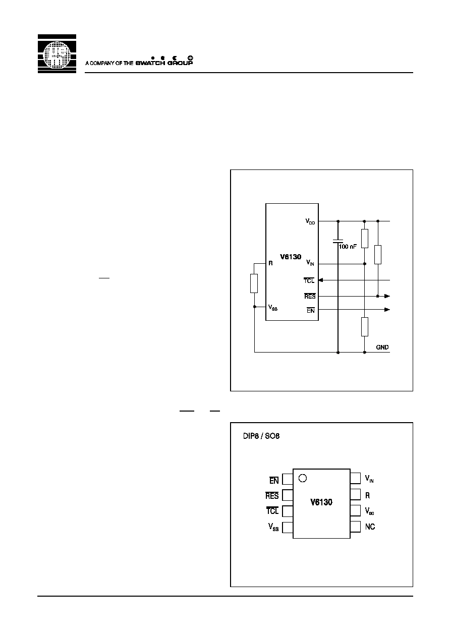
Typical Operating Configuration
Pin Assignment
Fig. 1
Fig. 2
Absolute Maximum Ratings
Parameter
Symbol Conditions
Maximum voltage at V
DD
V
DDmax
V
SS
+ 8 V
Minimum voltage at V
DD
V
DDmin
V
SS
- 0.3 V
Max. voltage at any signal pin
V
MAX
V
DD
+ 0.3 V
Min. voltage at any signal pin
V
MIN
V
SS
- 0.3 V
Storage temperature
T
STO
-65 to +150 ∞C
Electrostatic discharge max. to
MIL-STD-883C method 3015
V
Smax
1000V
Max. soldering conditions
T
Smax
250 ∞C x 10 s
Ta ble 1
Stresses above these listed max i mum rat ings may cause
per ma nent dam age to the de vice. Ex po sure be yond
spec i fied op er at ing con di tions may af fect de vice re li abil -
ity or cause mal func tion.
Handling Procedures
This de vice has built-in pro tec tion against high static volt -
ages or elec tric fields; how ever, anti-static pre cau tions
must be taken as for any other CMOS com po nent. Un less
oth er wise spec i fied, proper op er a tion can only oc cur
when all ter mi nal volt ages are kept within the sup ply volt -
age range. Un used in puts must al ways be tied to a de -
fined logic volt age level.
Operating Conditions
Parameter
Symbol Min. Max. Units
Operating temperature
1)
TJ
-40
+125
∞C
Supply voltage
2)
V
DD
1.2
7
V
RES & EN guaranteed
3)
V
DD
1.2
V
Comparator input voltage
V
IN
0
V
DD
V
RC-oscillator programming
R
10
1000
k
Ta ble 2
1)
The max i mum op er at ing tem per a ture is con firmed by sam pling
at ini tial de vice qual i fi ca tion. In pro duc tion, all de vices are
tested at +85 ∞C. On re quest de vices tested at +125 ∞C can
be sup plied.
2)
A 100 nF de coup ling ca pac i tor is re quired on the sup ply
volt age V
DD
for sta bil ity.
3)
RES must be pulled up ex ter nally to V
DD
event if it is un used.
(Note: RES and EN are used as in puts by EM test.)
2
V6130
Electrical Characteristics
3.0
V
DD
5.5 V, C = 100 nF, T
A
= -40 to +85 ∞C, un less oth er wise spec i fied
Parameter
Symbol Test Conditions
Min.
Typ.
Max.
Unit
Supply current in standby mode
I
SS
R
EXT
= don't care, TCL = V
DD
,
V
IN
= 0 V
22
35
µA
Supply current
I
SS
R
EXT
= 100 k
, I/Ps at V
DD
,
O/Ps 1 M
to V
DD
55
100
µA
RES and EN
Output Low Voltage
V
OL
V
DD
= 4.5 V, I
OL
= 20 mA
0.4
V
V
OL
V
DD
= 4.5 V, I
OL
= 8 mA
0.2
0.4
V
V
OL
V
DD
= 2.0 V, I
OL
= 4 mA
0.2
0.4
V
V
OL
V
DD
= 1.2 V, I
OL
= 0.5 mA
0.06
0.2
V
EN
Output High Voltage
V
OH
V
DD
= 4.5 V, I
OH
= -1 mA
3.5
4.1
V
V
OH
V
DD
= 2.0 V, I
OH
= -100 µA
1.8
1.9
V
V
OH
V
DD
= 1.2 V, I
OH
= -30 µA
1.0
1.1
V
TCL and V
IN
TCL input low level
V
IL
V
SS
0.8
V
TCL input high level
V
IH
2.0
V
DD
V
Leakage current TCL input
I
LI
V
SS
V
TCL
V
DD
0.05
1
µA
V
IN
input resistance
R
VIN
100
M
Comparator reference
1)
V
REF
T
A
= +25 ∞C
1.148
1.170
1.200
V
V
REF
T
A
= -20 to +70 ∞C
1.123
1.218
V
V
REF
1.123
1.222
V
Comparator hysteresis
1)
V
HY
2
mV
Ta ble 3
1)
The com para tor ref er ence is the power-down re set thresh old. The power-on re set thresh old equals the com para tor ref er ence
volt age plus the com para tor hys ter esis (see Fig.5).

3
V6130
Timing Characteristics
V
DD
= 5.0 V ± 3%, C = 100 nF, T
A
= -40 to +85∞C, un less oth er wise spec i fied
Parameter
Symbol Test Conditions
Min.
Typ.
Max.
Units
Propagation delays:
TCL to Output Pins
T
DIDO
250
500
ns
V
IN
sensitivity
T
SEN
1
5
20
µs
Logic Transition Times on all
Output Pins
T
TR
Load 10 k
, 50 pF
30
100
ns
Power-on Reset delay
T
POR
R
EXT
= 118 k
, ± 1%
90
100
110
ms
Watchdog Time
T
WD
R
EXT
= 118 k
, ± 1%
90
100
110
ms
Open Window Percentage
OWP
±0.2 T
WD
Closed Window Time
T
CW
0.8 T
WD
T
CW
R
EXT
= 118 k
, ± 1%
72
80
88
ms
Open Window Time
T
OW
0.4 T
WD
T
OW
R
EXT
= 118 k
, ± 1%
36
40
44
ms
Watchdog Reset Pulse
T
WDR
T
WD
/ 40
T
WDR
R
EXT
= 118 k
, ± 1%
2.5
ms
T
CL
Input Pulse Width
T
TCL
150
ns
Ta ble 4
Timing Waveforms
Watchdog Timeout Period
Fig. 4
I
SS
Standby versus Temperature at V
DD
= 5.5 V
Fig. 3

4
V6130
Timer Reaction
Combined Voltage and Timer Reaction
Fig. 6
Fig. 7
Voltage Monitoring
Fig. 5

Pin Description
Pin
Name
Function
1
EN
Push-pull active low enable output
2
RES
Open drain active low reset output.
RES must be pulled up to V
DD
even
if unused
3
TCL
Watchdog timer clear input signal
4
V
SS
GND terminal
5
NC
No connection
6
V
DD
Voltage supply
7
R
R
EXT
input for RC oscillator tuning
8
V
IN
Voltage comparator input
Ta ble 5
Functional Description
V
IN
Monitoring
The power-on re set and the power-down re set are gen er -
ated as a re sponse to the ex ter nal volt age level on the V
IN
in put. The ex ter nal volt age level is typ i cally ob tained from
a volt age di vider as shown in Fig. 9. The user de fines an
ex ter nal volt age di vider to set the de sired thresh old level
for power-on re set and power-down re set in his sys tem.
The in ter nal com para tor ref er ence volt age is typ i cally
1.17 V.
At power-up the re set out put (RES) is held low (see Fig.
5). When V
IN
be comes greater than V
REF
, the RES out put is
held low for an ad di tional power-on re set (POR) de lay
which is equal to the watch dog time T
WD
(typ i cally 100 ms
with an ex ter nal re sis tor of 118 k
con nected at R pin).
The POR de lay pre vents re peated tog gling of RES even if
V
IN
and the INPUT volt age drops out and re cov ers. The
POR de lay al lows the mi cro pro ces sor's crys tal os cil la tor
time to start and sta bi lize and en sures cor rect rec og ni tion
of the re set sig nal to the mi cro pro ces sor.
The RES out put goes ac tive low gen er at ing the
power-down re set when ever V
IN
falls be low V
REF
. The sen -
si tiv ity or re ac tion time of the in ter nal com para tor to the
volt age level on V
IN
is typ i cally 5 µs.
Timer Programming
The on-chip os cil la tor needs an ex ter nal re sis tor R
EXT
con -
nected be tween the R pin and V
SS
(see Fig. 9). It al lows
the user to ad just the power-on re set (POR) de lay, watch -
dog time T
WD
and with this also the closed and open time
win dows as well as the watch dog re set pulse width
(T
WD
/40).
With R
EXT
= 118 k
, the typ i cal de lays are:
- Power-on re set de lay: T
POR
is 100 ms
- Watch dog time:
T
WD
is 100 ms
- Closed win dow:
T
CW
is 80 ms
- Open win dow:
T
OW
is 40 ms
- Watch dog re set:
T
WDR
is 2.5 ms
Note: The cur rent con sump tion in creases as the fre -
quency in creases.
Watchdog Timeout Period Description
The watch dog time out pe riod is di vided into two parts, a
"closed" win dow and an "open" win dow (see Fig.4) and is
de fined by two pa ram e ters, T
WD
and the Open Win dow
Per cent age (OWP).
The closed win dow starts just af ter the watch dog timer re -
sets and is de fined by T
CW
= T
WD
- OWP(T
WD
).
The open win dow starts af ter the closed time win dow fin -
ishes and lasts till T
WD
+ OWP(T
WD
). The open win dow
time is de fined by T
OW
= 2 x OWP(T
WD
).
For ex am ple if T
WD
= 100 ms (ac tual value) and OWP =
±20% this means the closed win dow lasts dur ing first the
80 ms (T
CW
= 80 ms = 100 ms - 0.2 (100 ms)) and the
open win dow the next 40 ms (T
OW
= 2 x 0.2 (100 ms) = 40
ms). The watch dog can be ser viced be tween 80 ms and
120 ms af ter the timer re set. How ever as the time base is
±10% ac cu rate, soft ware must use the fol low ing cal cu la -
tion for ser vic ing sig nal TCL dur ing the open win dow:
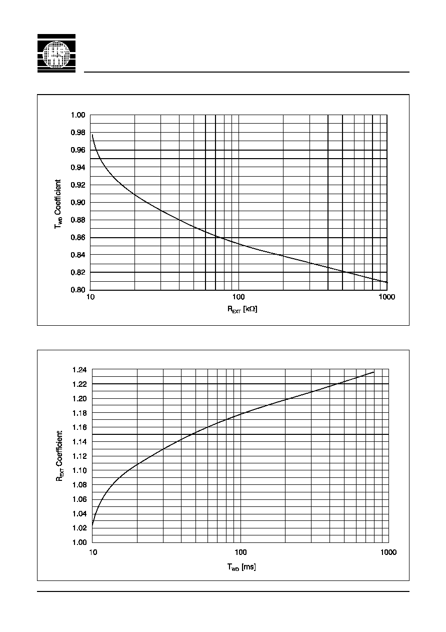
Re lated to curves (Fig. 10 to Fig. 20), es pe cially Fig. 19
and Fig. 20, the re la tion be tween T
WD
and R
EXT
could
easily be de fined. Let us take an ex am ple de scrib ing the
vari a tions due to pro duc tion and tem per a ture:
1. Choice, T
WD
= 26 ms.
2. Re lated to Fig. 20, the co ef fi cient (T
WD
to R
EXT
) is 1.125
where R
EXT
is in k
and T
WD
in ms.
3. R
EXT
(typ.) = 26 x 1.125 = 29.3 k
.
5
V6130
Block Diagram
Fig. 8
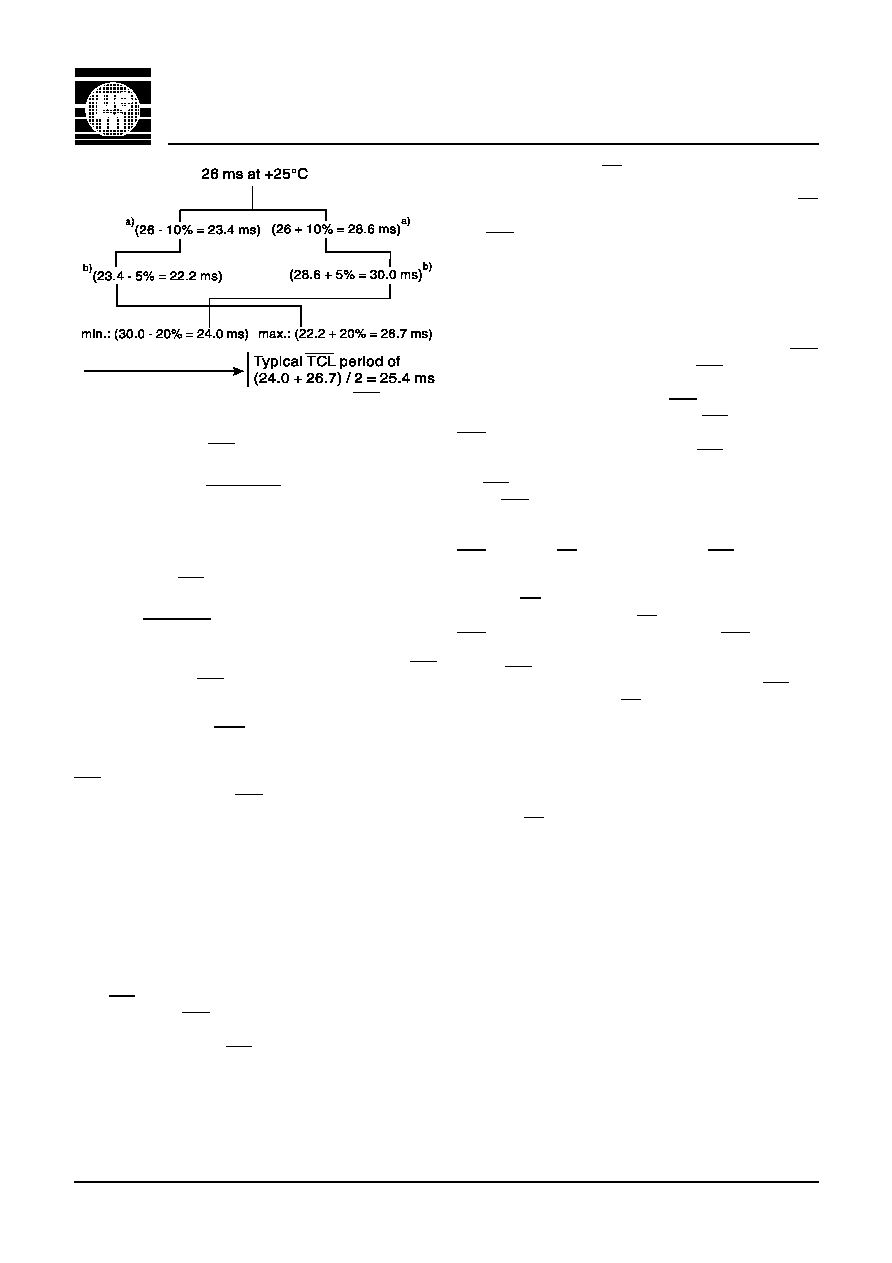
V6130
4.
The ra tio be tween T
WD
= 26 ms and the (TCL pe riod)
= 25.4 ms is 0.975.
Then the re la tion over the pro duc tion and the full tem -
per a ture range is, TCL pe riod = 0.975 x T
WD
0.975 x R
EXT
or TCL pe riod = , as typ i cal value.
1.125
a) While PRODUCTION value un known for the cus-
tomer when R
EXT
118 k
.
b) While op er at ing TEMPERATURE range
-40 ∞C
T
A
+85 ∞C.
5. If you fixed a TCL pe riod = 26 ms
26 x 1.125
R
EXT
= 30 k
.
0.975
If dur ing your pro duc tion the T
WD
time can be mea -
sured at T
A
= +25 ∞C and the µC can ad just the TCL
pe riod, then the TCL pe riod range will be much larger
for the full op er at ing tem per a ture.
Timer Clear ing and RES Ac tion
The watch dog cir cuit mon i tors the ac tiv ity of the pro ces -
sor. If the user's soft ware does not send a pulse to the
TCL in put within the pro grammed open win dow time out
pe riod, a short watch dog RES pulse is gen er ated which is
equal to T
WD
/40 = 2.5 ms typ i cally (see Fig. 6).
With the open win dow con straint, new se cu rity is added
to con ven tional watch dogs by mon i tor ing both soft ware
cy cle time and ex e cu tion. Should soft ware clear the
watch dog too quickly (in cor rect cy cle time) or too slowly
(in cor rect ex e cu tion), it will cause the sys tem to be re set.
If the soft ware is stuck in a loop which in cludes the rou tine
to clear the watch dog, a con ven tional watch dog will not
re set the sys tem even though the soft ware is mal func tion -
ing; the V6130 will gen er ate a sys tem re set be cause the
watch dog is cleared too quickly.
If no TCL signal is ap plied be fore the closed and open
win dows ex pire, RES will start to gen er ate square waves
of pe riod (T
CW
+ T
OW
+ T
WDR
). The watch dog will re main in
this state un til the next TCL fall ing edge ap pears dur ing
an open win dow, or un til a fresh power-up se quence. The
sys tem en able out put, EN, can be used to pre vent crit i cal
con trol func tions be ing ac ti vated in the event of the sys -
tem go ing into this fail ure mode (see sec tion "En able - EN
Out put").
The RES out put must be pulled up to V
DD
even if the out -
put is not used by the sys tem (see Fig. 9)
Com bined Volt age and Timer Ac tion
The com bi na tion of volt age and timer ac tions is il lus -
trated by the se quence of events shown in Fig. 7. On
power-up, when the volt age at V
IN
reaches V
REF
, the
power-on-reset, POR, de lay is in i tial ized and holds RES
ac tive for the time of the POR de lay. A TCL pulse will have
no ef fect un til this power-on-reset de lay is com pleted. Af -
ter the POR de lay has elapsed, RES goes in ac tive and
the watch dog timer starts act ing. If no TCL pulse oc curs,
RES goes ac tive low for a short time T
WDR
af ter each
closed and open win dow pe riod. A TCL pulse com ing
dur ing the open win dow clears the watch dog timer. When
the TCL pulse oc curs too early (dur ing the closed win -
dow), RES goes ac tive and a new time out se quence
starts. A volt age drop be low the V
REF
level for lon ger than
typ i cally 5 µs, over rides the timer and im me di ately forces
RES ac tive and EN in ac tive. Any fur ther TCL pulse has no
ef fect un til the next power-up se quence has com pleted.
En able - EN Out put
The sys tem en able out put, EN, is in ac tive al ways when
RES is ac tive and re mains in ac tive af ter a RES pulse un til
the watch dog is ser viced cor rectly 3 con sec u tive times
(ie. the TCL pulse must come in the open win dow). Af ter
three con sec u tive ser vices of the watch dog with TCL dur -
ing the open win dow, the EN goes ac tive low. A mal func -
tion ing sys tem would be re peat edly re set by the
watch dog. In a con ven tional sys tem crit i cal mo tor con -
trols could be en er gized each time re set goes in ac tive
(time al lowed for the sys tem to re start) and in this way the
elec tri cal mo tors driven by the sys tem could func tion out
of con trol. The V6130 pre vents the above fail ure mode by
us ing the EN out put to dis able the mo tor con trols un til
soft ware has suc cess fully cleared the watch dog three
times (ie. the sys tem has cor rectly re started af ter a re set
con di tion).
6

7
V6130
Typical Application
R
Fig. 9

8
V6130
T
WD
versus Temperature at 5 V
T
WD
versus V
DD
at T
A
= +25∞C
T
WD
versus R at T
A
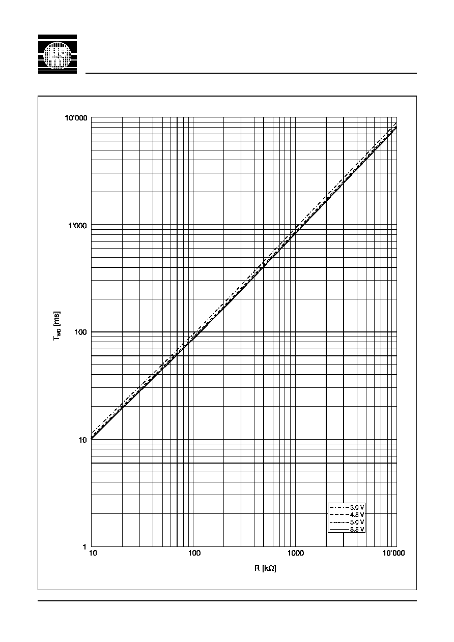
= +25∞C
Fig. 10
T
WD
versus R at 5 V
Fig. 11
Fig. 12
Fig. 13
T
WD
versus R at T
A
= +25 ∞C
9
V6130
Fig. 14

10
V6130
T
WD
versus V
DD
at T
A
= +85∞C
T
WD
versus V
DD
at T
A
= -40∞C
T
WD
versus R at T
A
= +85∞C
T
WD
versus R at T
A
= -40∞C
Fig. 15
Fig. 16
Fig. 17
Fig. 18
11
V6130
T
WD
Coefficient versus R
EXT
at T
A
= +25∞C
R
EXT
Coefficient versus T
WD
at T
A
= +25∞C
Fig. 19
Fig. 20

12
V6130
Package and Ordering Information
Dimensions of DIP8 Package
Fig. 21
Dimensions of SO8 Package
Di men sions in mm
Dimensions in mm
Fig. 22
Ordering Information
The V6130 is avail able in the fol low ing pack ages:
Type Pack age
V6130 8P DIP8
V6130 8S SO8
When ordering please specify complete part num ber.
EM Mi cro elec tronic-Marin SA can not as sume re spon si bil ity for use of any cir cuitry de scribed other than cir cuitry en tirely em bod ied in
an EM Mi cro elec tronic-Marin SA prod uct. EM Mi cro elec tronic-Marin SA re serves the right to change the cir cuitry and spec i fi ca tions
with out no tice at any time. You are strongly urged to en sure that the in for ma tion given has not been su per seded by a more up-to-date
ver sion.
E. & O.E. Printed in Switzerland, Th © 2000 EM Microelectronic-Marin SA, 10/00, Rev. D/330
EM MICROELECTRONIC-MARIN SA, CH-2074 Marin, Switzerland, Tel. 032 - 755 51 11, Fax 032 - 755 54 03