 | –≠–ª–µ–∫—Ç—Ä–æ–Ω–Ω—ã–π –∫–æ–º–ø–æ–Ω–µ–Ω—Ç: V6309 | –°–∫–∞—á–∞—Ç—å:  PDF PDF  ZIP ZIP |

3-Pin Microprocessor Reset Circuit
Fea tures
n
Precision monitoring of 3 V, 3.3 V and 5 V power
supply voltages
n
Fully specified over the temperature range of
-40 to + 125
o
C
n
140 ms minimum power-on reset pulse width:
RESET output for V6309
RESET output for V6319
n
16 µA supply current
n
Garanteed RESET/RESET valid to V
DD
= 1 V
n
Power supply transient immunity
n
No external components needed
n
3-pin SOT-23 package
n
Fully compatible with MAX809/MAX810 and
AMD809/AMD810
De scrip tion
The V6309 and V6319 are mi cro pro ces sor su per vi sory cir -
cuits used to mon i tor the power sup plies in µP and dig i tal
sys tems. They pro vide ex cel lent cir cuit re li abil ity and low
cost by elim i nat ing ex ter nal com po nents and ad just ments
when used with 5 V pow ered or 3 V pow ered cir cuits.
These cir cuits per form a sin gle func tion: they as sert a re -
set sig nal when ever the V
DD
sup ply volt age de clines be low
a pre set thresh old, keep ing it as serted for at least 140 ms
af ter V
DD
has risen above the re set thresh old. The only dif -
fer ence be tween the two de vices is that the V6309 has an
ac tive-low RESET out put (which is guar an teed to be in the
cor rect state for V
DD
down to 1 V), while the V6319 has an
ac tive-high RESET out put. The re set com para tor is de -
signed to ig nore fast tran sients on V
DD
. Re set thresh olds
suit able for op er a tion with a va ri ety of sup ply volt ages are
avail able.
Low sup ply cur rent makes the V6309/V6319 ideal for use
in por ta ble equip ment. The V6309/V6319 come in a 3-pin
SOT-23 pack age
Ap pli ca tions
n
Computers
n
Controllers
n
Intelligent instruments
n
Critical µP and µC power monitoring
n
Portable/battery-powered equipment
1
V6309/V6319
Æ
Typi cal Op er at ing Con figu ra tion
Pin As sign ment
Fig. 2
Fig. 1
EM MICROELECTRONIC-MARIN SA

Ab so lute Maxi mum Rat ings
Pa rame ter
Sym bol Con di tions
Terminal voltage to V
SS
V
DD
-0.3 to 6.0 V
Min. voltage at Reset or Reset
V
min
-0.3 V
Max. voltage at Reset or
Reset
V
max
V
CC
+ 0.3 V
Input current at V
DD
I
min
20 mA
Output current at Reset or Reset I
max
20 mA
Rate of rise at V
DD
t
R
100 Vµs
Continuous power dissipation
P
max
320 mW
at T
A
= +70 ∞C for SOT-23
(>70 ∞C derate by 4 mW /∞C)
Operating temperature range
T
A
-40 to +125 ∞C
Storage temperature range
T
ST
-65 to +150 ∞C
Ta ble 1
Stresses above these listed max i mum rat ings may cause
per ma nent dam age to the de vice. Ex po sure be yond spec -
i fied op er at ing con di tions may af fect de vice re li abil ity or
cause mal func tion.
Han dling Pro ce dures
This de vice has built-in pro tec tion against high static volt -
ages or elec tric fields; how ever, anti-static pre cau tions
must be taken as for any other CMOS com po nent. Un less
oth er wise spec i fied, proper op er a tion can only oc cur
when all ter mi nal volt ages are kept within the sup ply volt -
age range.
2
V6309/V6319
Æ
Pa ram e ter
Sym bol Test Con di tions
Min.
Typ.
Max.
Units
V
DD
range
V
DD
T
A
= 0 to +70 ∞C
1.0
5.5
V
T
A
= -40 to +105 ∞C
1.2
5.5
V
T
A
= -40 to +125 ∞C
1.6
5.5
V
Sup ply cur rent ver sions L, M
I
CC
V
DD
< 5.5 V
26
60
µA
ver sions R,S,T
V
DD
< 3.6 V
16
50
µA
Re set thresh old
1)
ver sion L
V
TH
T
A
= +25 ∞C
4.56
4.63
4.70
V
T
A
= -40 to +125 ∞C
4.40
4.79
V
ver sion M
T
A
= +25∞C
4.31
4.38
4.45
V
T
A
= -40 to +125 ∞C
4.16
4.53
V
ver sion T
T
A
= +25∞C
3.04
3.08
3.11
V
T
A
= -40 to +125∞C
2.92
3.17
V
ver sion S
T
A
= +25 ∞C
2.89
2.93
2.96
V
T
A
= -40 to +125 ∞C
2.78
3.02
V
ver sion R
T
A
= +25 ∞C
2.59
2.63
2.66
V
T
A
= -40 to +125∞C
2.50
2.72
V
Re set thresh old temp. co ef fi cient
-200
ppm/∞C
V
DD
to re set de lay
1)
V
DD
= V
TH
to (V
TH
- 100 mV)
7
µs
Re set ac tive time out pe riod
T
A
= -40 to +125 ∞C
140
330
590
ms
Re set out put volt age low for V6309
V
OL
V
DD
> 1.0 V, I
SINK
= 50 µA
0.3
V
ver sions R,S,T
V
DD
= V
TH
min., I
SINK
= 1.2 mA
0.3
V
ver sions L, M
V
DD
= V
TH
min., I
SINK
= 3.2 mA
0.4
V
Re set out put volt age high for V6309
ver sions R,S,T V
OH
V
DD
> V
TH
max., I
SOURCE
= 500 µA
0.8 V
DD
V
ver sions L, M
V
DD
> V
TH
max., I
SOURCE
= 800 µA
V
DD
-1.5 V
V
Re set out put volt age low for V6319
ver sions R,S,T V
OL
V
DD
= V
TH
max., I
SINK
= 1.2 mA
0.3
V
ver sions L, M
V
DD
= V
TH
max., I
SINK
= 3.2 mA
0.4
V
I
SOURCE
= 150 µA
Elec tri cal Char ac ter is tics
V
DD
= full range, T
A
= -40 to +125 ∞C un less oth er wise spec i fied, typ i cal val ues are at T
A
= +25 ∞C, V
DD
= 5 V for ver sions L and
M, V
DD
= 3.3 V for ver sions T and S, V
DD
= 3 V for ver sion R.(Pro duc tion test ing done at T
A
= +25∞C and 85 ∞C, over tem per a ture
lim its guar an teed by de sign only)
1)
Re set out put for V6309, Re set out put for V6319 Ta ble 2

3
V6309/V6319
Æ
Sup ply Cur rent vs. Tem pera ture
No load, V63xxR/S/T
Power-Up Re set Time out vs. Tem pera ture
All ver sions
Sup ply Cur rent vs. Tem pera ture
No load, V63xxL/M
Power-Down Re set Delay vs. Tem pera ture
V63xxL/M
Nor mal ized Re set Threshold vs. Tem per a ture
All ver sions
Power- Down Re set De lay vs. Tem pera ture
V63xxR/S/T
Fig. 8
Fig. 5
Fig. 7
Fig. 4
Fig. 6
Fig. 3

Pin De scrip tion
Ta ble 3
Ap pli ca tion In for ma tion
Neg a tive-Going V
DD
Tran sients
In ad di tion to is su ing a re set to the mi cro pro ces sor dur ing
power-up, power-down, and brown out con di tions, the
V6309/V6319 are rel a tively im mune to short du ra tion neg -
a tive-going V
DD
tran sients (glitches). Fig. 8 shows typ i cal
tran sient du ra tion vs. Re set com para tor over drive, for
which the V6309/V6319 do not gen er ate a re set pulse. The
graph was gen er ated us ing a neg a tive-going pulse ap -
plied to V
DD
, start ing 0.5 V above the ac tual re set thresh old
and end ing be low it by the mag ni tude in di cated (re set
com para tor over drive). The graph in di cates the max i mum
pulse width a neg a tive-going V
DD
tran sient can have with -
out caus ing a re set pulse. As the mag ni tude of the tran -
sient in creases (goes far ther be low the re set thresh old),
the max i mum al low able pulse width de creases. Typically,
for the V6309L and V6319M, a V
DD
tran sient that goes 100
mV be low the re set thresh old and lasts 20 µs or less will
not cause a re set pulse. A 0.1 µF by pass ca pac i tor
mounted as close as pos si ble to the V
DD
pin pro vides ad di -
tional tran sient im mu nity.
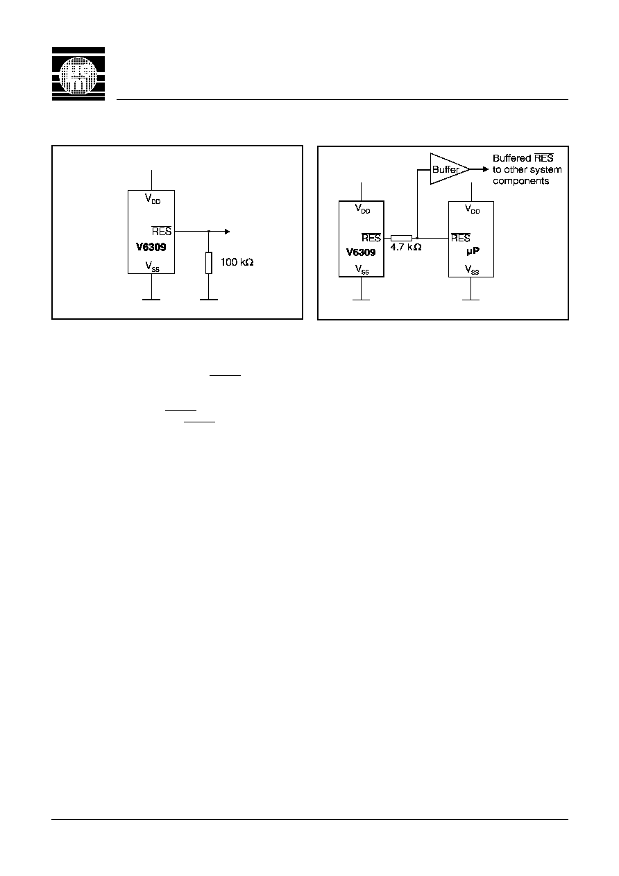
En suring a Valid Re set Out put down to V
DD
= 0 V
When V
DD
falls be low 1 V, the V6309 RESET out put no lon -
ger sinks cur rent, it be comes an open cir cuit. There fore,
high-impedance CMOS logic in puts con nected to RESET
can drift to un de ter mined volt ages. This pres ents no prob -
lem in most ap pli ca tions, since most µP and other cir cuitry
is in op er a tive with V
DD
be low 1 V. How ever, in ap pli ca tions
where RESET must be valid down to 0 V, add ing a
pull-down re sis tor to RESETcauses any stray leak age cur -
rents to flow to ground, hold ing RESET low (Fig.10). R1's
value is not crit i cal; 100 k
is large enough not to load
RESET and small enough to pull RESET to ground. A 100
k
pull-up re sis tor to V
DD
is also rec om mended for the
V6319, if RESET is re quired to re main valid for V
DD
<1 V.
4
V6309/V6319
Æ
Pin
Name
Func tion
1
V
SS
Ground
2 for V6309
RESET Out put re mains low while V
DD
RESET
is be low the re set thresh old and rises
for 240 ms af ter V
DD
above the re set
thresh old
2 for V6319
RESET Out put re mains high while V
DD
RESET
is be low the re set thresh old and rises
for 240 ms af ter V
DD
above the re set
3
V
DD
Sup ply volt age (+5V, +3.3V or +3.0V )
Max.Transient Du ra tion with out Causing a Re set
Pulse ver sus Re set Com para tor Overdrive
Fig. 9
5
V6309/V6319
Æ
RESET Valid for V
DD
= Ground Cir cuit
Fig. 10
In ter fac ing to µPs with Bidi rec tional Reset I/O
Fig. 11
In ter facing to µPs with Bidirectional Re set Pins
Mi cro pro ces sors with bidirectional re set pins (such as the
Motorola 68HC11 se ries) can con nect to the V6309 re set
out put. If, for ex am ple, the V6309 RESET out put is as -
serted high and the µP wants to pull it low, in de ter mi nate
logic lev els may re sult. To cor rect this, con nect a 4.7 k
re -
sis tor be tween the V6309 RESET out put and the µP re set
I/O (Fig. 11). Buffer the V6309 RESET out put to other sys -
tem com po nents.
Ben e fits of Highly Ac cu rate Re set Thresh old
Most µP su per vi sor ICs have re set thresh old volt ages be -
tween 5% and 10% be low the value of nom i nal sup ply
volt ages. This en sures a re set will not oc cur within 5% of
the nom i nal sup ply, but will oc cur when the sup ply is 10%
be low nom i nal. When us ing ICs rated at only the nom i nal
sup ply ±5%, this leaves a zone of un cer tainty where the
sup ply is be tween 5% and 10% low, and where the re set
may or may not be as serted.
The V6309L/T and V6319L/T use highly ac cu rate cir cuitry
to en sure that re set is as serted close to the 5% limit, and
long be fore the sup ply has de clined to 10% be low nom i -
nal.

6
V6309/V6319
Æ
Mark ing In for ma tion
Marking code
Type number
EL
V6309L
EM
V6309M
ET
V6309T
ES
V6309S
ER
V6309R
1)
FL
V6319L
FM
V6319M
FT
V6319T
FS
V6319S
FR
V6319R
Ta ble 5
Ver sion Let ter Defi ni tion
Out put stage
Thresh old Volt age [V]
4.63 4.38 3.08 2.93 2.63
V6309, RESET out put
L
M
T
S
R
V6319
1)
, RESET out put
L
M
T
S
R
Ta ble 4
Or der ing In for ma tion
The V6309 is avail able with a RESET out put, the V6319
with a RESET out put. Both type come in a 3-pin SOT-23
pack age.
Or der ing form: Type num ber<ver sion let ter><pack age>
When or der ing, please al ways spec ify the com plete part
number
Pack age and Or der ing In for ma tion
1)
Non-stock items for V6319
EM Mi cro elec tronic-Marin SA can not as sume any re spon si bil ity for use of any cir cuitry de scribed other than
en tirely em bod ied in an EM Mi cro elec tronic-Marin SA prod uct. EM Mi cro elec tronic-Marin SA re serves the right to
change the cir cuitry and spec i fi ca tions with out no tice at any time. You are strongly urged to en sure that the
in for ma tion given has not been su per seded by a more up-to-date ver sion.
E. & O.E. Printed in Swit zer land, Th
© 2000 EM Mi cro elec tronic-Marin SA, 10/00, Vers. B/323
EM Mi cro elec tronic-Marin SA, CH - 2074 Marin, Swit zer land, Tel. (+41) 32 - 755 51 11, Fax (+41) 32 - 755 54 03