 | –≠–ª–µ–∫—Ç—Ä–æ–Ω–Ω—ã–π –∫–æ–º–ø–æ–Ω–µ–Ω—Ç: V6330 | –°–∫–∞—á–∞—Ç—å:  PDF PDF  ZIP ZIP |

Applications
All microprocessor applications where an automatic restart is
required:
Computer electronics
n
White / Brown goods
Automotive electronics
Industrial electronics
n
n
n
n
n
Telecom systems
Hand-held systems
1
Features
n
n
n
n
n
n
n
n
n
n
n
Voltage Window monitoring
Processor reset at power down
Reset output guaranteed down to V
= 1 V
C
C
TO-92 package
Pin compatible with MC 33164
DD
O
O
n
Clear microprocessor restart after power up
Low power consumption: typ. 3 A at V
= 5 V
- 40 to +85
temperature range
On request extended temperature range, -40 to +125
On-chip oscillator
No external components required
Push-pull or Open drain output
µ
DD
Description
The V6330 is a CMOS device which monitors the supply voltage
of any electronic system, and generates the appropriate Reset
signal.
The gap between the two thresholds defines the
allowed voltage range. As long as V stays inside this voltage
window, the output stays inactive. If V drops below V
, or
rises above V
, the output gets active. When V enters into
the allowed range, the output remains active for an additional 50
ms (typ.). This allows the system to stabilize before getting fully
active. The lower threshold voltage may be obtained in
different versions:
2.0 V to 6 V
2.4 V to 6 V
2.8 V to 6 V
3.5 V to 6 V
4.0 V to 6 V
4.5 V to 6 V
DD
THlow
THhigh
DD
DD
3-Pin Microprocessor Reset with Time-out
and Voltage Window
Typical Operating Configuration
Pin Assignment
EM MICROELECTRONIC-MARIN SA
V6330
Handling Procedures
Stresses above these listed maximum ratings may cause
permanent damage to the device. Exposure beyond specified
operating conditions may affect device reliability or cause
malfunction.
1)
The maximum operating temperature is confirmed by
sampling at initial device qualification.
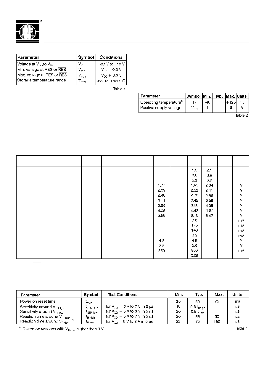
2
Absolute Maximum Ratings
This device has built-in protection against high static voltages
or electric fields; however, anti-static precautions must be taken
as for any other CMOS component.
Unless otherwise
specified, proper operation can only occur when all terminal
voltages are kept within the supply voltage range.
Operating Conditions
Electrical Characteristics
T = -40 to +85 C, unless otherwise specified
A
O
I
DD
V
HYS
V
OL
V
OL
V
OL
V
OH
V
OH
I
LEAK
V
= 2 V
DD
V
= 5 V, I = 8 mA
OL
DD
V
= 5.5 V
DD
Supply current
1)
Threshold Low Voltage
Threshold hysteresis
RES Output Low Level
RES Output High Level
Output leakage current
2)
µ
A
µ
A
µ
A
µ
A
Parameter
Symbol
Test Conditions
Min.
Typ.
Max.
Units
I
DD
V
= 5 V
DD
V
= 8 V
DD
Version: A,G,M
Version: B,H,N
Version: C,I,O
Version: D,J,P
Version: E,K,Q
Version: F,L,R
I
DD
V
TH low
V
TH low
Max.
at 25
O
C
Min.
at 25
O
C
V
OH
V
= 3 V, I = 4 mA
DD
OL
V
= 1 V, I = 50 A
µ
DD
OL
V
= 5 V, I
= -8 mA
DD
OH
V
= 3 V, I
= -4 mA
DD
OH
V
= 1 V, I
= -100 A
µ
DD
OH
1.84
2.18
2.59
3.23
3.70
4.22
5.79
3.1
5.7
10.0
2.17
2.55
3.03
3.80
4.32
4.95
6.82
400
300
90
1
1)
2)
RES or
open
Only for Open drain versions
RES
Table 3
Threshold High Voltage
V
TH low
V
TH low
V
TH low
V
TH low
V
TH high
Timing Characteristics
V
= 5.0 V, T = -40 to +85 C, unless otherwise specified
A
O
DD
V6330

3
Pin Description
TO-92
Block Diagram
Timing Waveforms
V
DD
V
THlow
1 V
Logic "1"
t
POR
t
Rhigh
t
POR
Fig.3
RES
RES
t
t
t
Logic "1"
Logic "0"
Logic "0"
t
SENhigh
t
Rlow
V
THhigh
t
SENlow
Fig.4
RES or RES
V
DD
V
ss
Voltage
Reference
Reset
Logic
Oscillator
Timer
V6330

4
Ordering Information
V6330 P TO-92
The V6330 is available with Push-pull or Open output stage
and Reset active low or high.
Ordering form: V6330 <version letter> < packaging>
Example: Smart reset with: - Reset active low
- Open drain output
- 3.5 V threshold
- TO-92 package
When ordering, please specify the complete part number.
Version letter definition
Output stage
Threshold Low Voltage [V]
2.0 2.4 2.8 3.5 4.0 4.5
Push-pull, Reset active low
A
B
C
D
E
F
1)
1)
1)
1)
Push-pull, Reset active high G
H
I
J
K
L
1)
1)
1)
1)
1)
1)
Open drain, Reset active low M
N
O
P
Q
R
1)
1)
1)
1)
1)
Table 6
Chip form on request
Non-stock items, minimum order 30 K pieces.
1)
V6330
EM Microelectronic-Marin SA cannot assume responsibility for use of any circuitry described other than circuitry entirely embodied in
an EM Microelectronic-Marin SA product. EM Microelectronic-Marin SA reserves the right to change the circuitry and specifications
without notice at any time. You are strongly urged to ensure that the information given has not been superseded by a more up-to-date
©
2000 EM Microelectronic-Marin SA, 10/00, Rev. D/319