2
Jan 31, 2005
SAW Components
B3855
169,00 MHz
Low Loss Filter
Data Sheet
Ceramic package QCC10B
Features
q
IF filter for WCDMA
q
Low insertion loss
q
Ceramic SMD package
Terminals
q
Gold plated
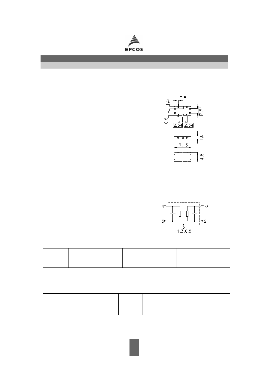
Dimensions in mm, appr. weight 0,23 g
Pin configuration
9, 10
Balanced Input
4, 5
Balanced Output
1, 3, 6, 8
Case ground
2, 7
To be grounded
Electrostatic Sensitive Device (ESD)
Type
Ordering code
Marking and Package
according to
Packing
according to
B3855
B39171-B3855-Z710
C61157-A7-A49
F61074-V8172-Z000
Maximum ratings
Operable temperature range
T
A
-40 / +85
∞C
Storage temperature range
T
stg
-40 / +85
∞C
DC voltage
V
DC
0
V
Source power
P
s
10
dBm

3
Jan 31, 2005
SAW Components
B3855
169,00 MHz
Low Loss Filter
Data Sheet
Characteristics
Operating temperature:
T
A
= -40 ... +85 ∞C
Terminating source impedance:
Z
S
= 200
and matching network
Terminating load impedance:
Z
L
= 200
and matching network
Group delay aperture:
150 kHz
min.
typ.
max.
Nominal frequency
f
N
--
169,00
--
MHz
Minimum insertion attenuation
min
1,5
2,0
3,5
dB
(including matching network)
Passband width
rel
1 dB
B
1dB
--
7,5
--
MHz
Amplitude ripple (p-p)
f
N
±
2,0 MHz
--
0,2
0,5
dB
Group delay ripple (p-p)
f
N
±
2,0 MHz
--
40
80
ns
Absolute group delay
mean value within
f
N
±
2,0 MHz
127
130
137
ns
Relative attenuation (relative to
min
)
rel
10 MHz
...
144 MHz
40
50
--
dB
144 MHz
...
148 MHz
20
40
--
dB
190 MHz
...
194 MHz
20
50
--
dB
194 MHz
...
2,0 GHz
40
45
--
dB
2,0 GHz
...
2,5 GHz
35
40
--
dB
VSWR
--
2,0:1
2,5:1
Impedance at f
N
(without matching)
Input: Z
IN
= R
IN
|| C
IN
--
690 || 1,3
--
||
pF
Output: Z
OUT
= R
OUT
|| C
OUT
--
580 || 1,1
--
||
pF
Temperature coefficient of frequency
TC
f
--
≠ 70
--
ppm/K
5
Jan 31, 2005
SAW Components
B3855
169,00 MHz
Low Loss Filter
Data Sheet
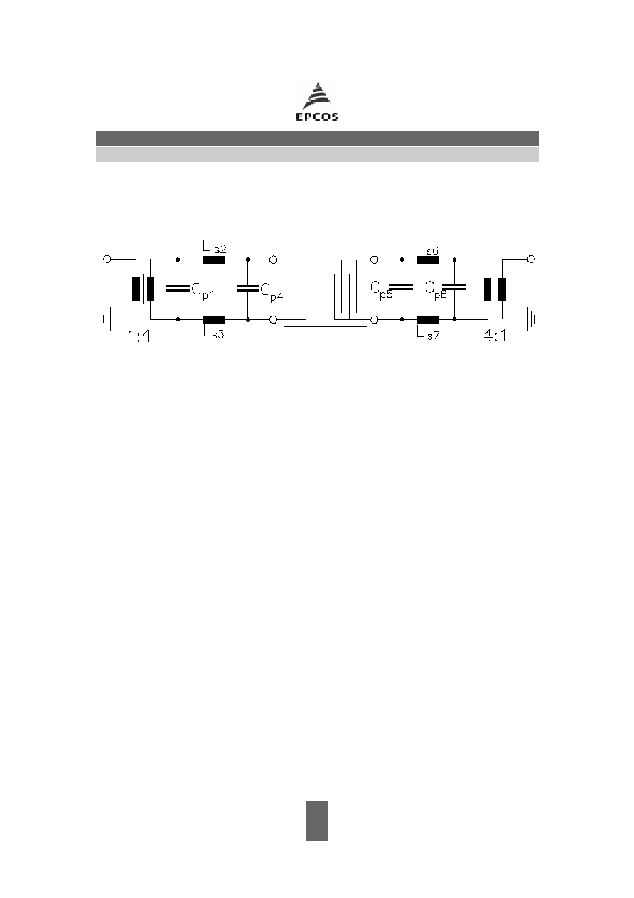
Matching network
(Element values depend upon PCB layout)
C
P1
=3,9 pF
C
P5
=1,0 pF
L
S2
=150 nH
L
S6
=150 nH
L
S3
=150 nH
L
S7
=180 nH
C
P4
=1,5 pF
C
P8
=3,3 pF
Published by EPCOS AG
Surface Acoustic Wave Components Division, SAW MC
P.O. Box 80 17 09, 81617 Munich, GERMANY
©
EPCOS AG 2004. Reproduction, publication and dissemination of this brochure and the informa-
tion contained therein without EPCOS' prior express consent is prohibited.
Purchase orders are subject to the General Conditions for the Supply of Products and Services of
the Electrical and Electronics Industry recommended by the ZVEI (German Electrical and Electronic
Manufacturers' Association), unless otherwise agreed.
This brochure replaces the previous edition.
For questions on technology, prices and delivery please contact the Sales Offices of EPCOS AG or
the international Representatives.
Due to technical requirements components may contain dangerous substances. For information on
the type in question please also contact one of our Sales Offices.