Metal Oxide Varistors
CT0603L25HSG
SMD multilayer varistor with Ni-barrier termination
B72500T8250L060
ISSUE DATE
28.01.2005
ISSUE
f
PUBLISHER
KB VS PE
PAGE
1/7
Designation system
CT
= Chip with three-layer- termination (Ag/Ni/Sn)
0603 = Dimensions of the device 06 x 03 (length x width in 1/100 inch)
L
= Tolerance of the varistor voltage (± 15%)
25
= Maximum operating voltage (RMS voltage)
HS
= Designed for protection of high speed data lines
G
= Taped version (cardboard tape, 7" reel, 4000 pieces/reel)
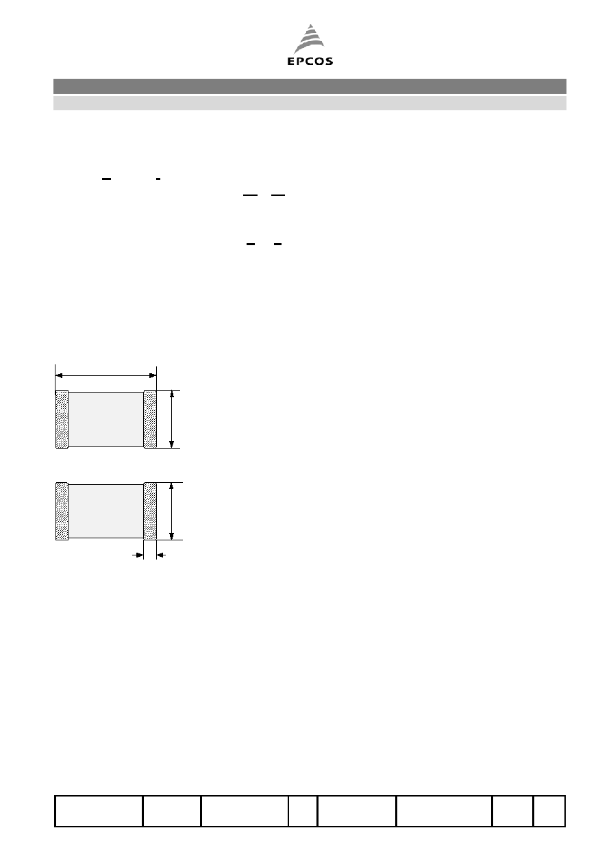
Figure
l = 1.6 ± 0.15
b = 0.8 ± 0.10
s = 0.9 max.
k = 0.1 ≠ 0.4
(all dimensions in mm)
As far as patents or other rights of third parties are concerned, liability is only assumed for components per se, not for
applications, processes and circuits implemented within components or assemblies. The information describes the type of
component and shall not be considered as assured characteristics. Terms of delivery and rights to change design reserved.
l
b
s
k

Metal Oxide Varistors
CT0603L25HSG
SMD multilayer varistor with Ni-barrier termination
B72500T8250L060
ISSUE DATE
28.01.2005
ISSUE
f
PUBLISHER
KB VS PE
PAGE
2/7
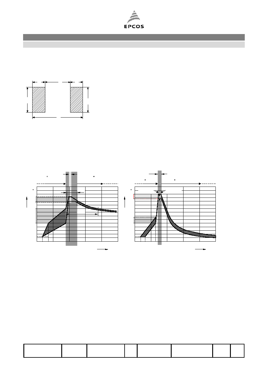
V-I-characteristic
10
-5
10
-4
10
-3
10
-2
10
-1
10
0
10
1
A
i
1
400
v
2
4
6
8
10
20
40
60
80
100
200
400
V
VAR9737A
100
0
10
20
30
40
50
60
70
80
90
%
-55
∞C
Ambient temperature
Max. current, energy, operating voltage and average power
dissipation depending on ambient temperature
70
80
90
100
110
120
130
140
150

Metal Oxide Varistors
CT0603L25HSG
SMD multilayer varistor with Ni-barrier termination
B72500T8250L060
ISSUE DATE
28.01.2005
ISSUE
f
PUBLISHER
KB VS PE
PAGE
3/7
Electrical data
Maximum operating voltage
RMS voltage
V
RMS
= 25 V
DC voltage
V
DC
= 32 V
Varistor voltage (@ 1 mA)
V
V
= 51.9 up to 70.1 V
Maximum clamping voltage (@ 1 A)
V
C
= 120 V
Maximum surge current (8/20 µs)
I
max
= 1 x 5 A
Maximum energy absorption (ESD)
E
max
= 50 mJ
(@ ESD according to ISO TR10605, 25 kV air discharge, 150 pF, 2 k)
Capacitance (@ 1 MHz, 1
V, 25 ∞C, typ.) C = 10 pF
Response time
< 0.5 ns
Operating temperature
-40 ... +125 ∞C
Storage temperature (mounted parts)
-40 ... +150 ∞C
Termination material
Ag/Ni/Sn
(thickness not specified, adjusted to fulfil wettability specification according to
IEC 60068-2-58)
Complies with following ESD standards:
IEC 61000-4-2 level 4 (8 kV contact, 15 kV air discharge)
ISO TR10605 level 4 (25 kV air discharge)
AEC Q200 002 level 6 (25 kV air discharge)

Metal Oxide Varistors
CT0603L25HSG
SMD multilayer varistor with Ni-barrier termination
B72500T8250L060
ISSUE DATE
28.01.2005
ISSUE
f
PUBLISHER
KB VS PE
PAGE
4/7
Stability to multiple ESD pulses
1)
0
20
40
60
80
0
1
10
100
1000
10000
number of ESD pulses
1)
15 kV air discharge, 150 pF, 330 , according to IEC 61000-4-2
Signal insertion loss
2)
-3.00
-2.50
-2.00
-1.50
-1.00
-0.50
0.00
0
20
40
60
80
100
frequency [MHz]
i
n
ser
t
i
on l
o
ss [
d
B
]
2)
typical values, measured with network analyzer HP8753 E/S containing S-parameter test set
Metal Oxide Varistors
CT0603L25HSG
SMD multilayer varistor with Ni-barrier termination
B72500T8250L060
ISSUE DATE
28.01.2005
ISSUE
f
PUBLISHER
KB VS PE
PAGE
5/7
Recommended geometry of solder pad
A = 1.0 mm
B = 1.0 mm
C = 1.0 mm
E = 3.0 mm
Recommended soldering temperature profile
100 s
at max. temp.
100
20
0
50
100
Preheating zone
max. 2
180
T
245
215
300
Soldering zone
max. 7 s
150
200
VAR0543-W-E
250
t
s
(natural air cooling)
40 s
max. 2
Cooling-down zone
C
C/s
C/s
2nd solder
Cooling-down zone
max. 5
100
20
0
50
100
1st solder
max. 2
Preheating zone
130
T
235
200
260
300
Soldering zone
max. 5 s
150
200
250
VAR0550-F-E
t
s
C
C/s
C/s (natural air cooling)
at max. temp.
10 s
wave
wave
This component should be soldered within 12 months after delivery from EPCOS. They
should be left in their original packings to avoid soldering problems due to oxidized terminals.
Storage temperature:
-25 to 45 ∞C
Relative humidity: < 75% annual average, < 95% on maximum 30 days in a year.
The usage of mild non-activated fluxes for soldering is recommended, as well as proper
cleaning of the PCB.
The components are suited for Pb-free soldering.
A
A
D
C
B
B