EG2121 LVDS Rev 1.4 35D
2.5V operation LVDS SAW Oscillator
EG-2121CA-L
Features
∑
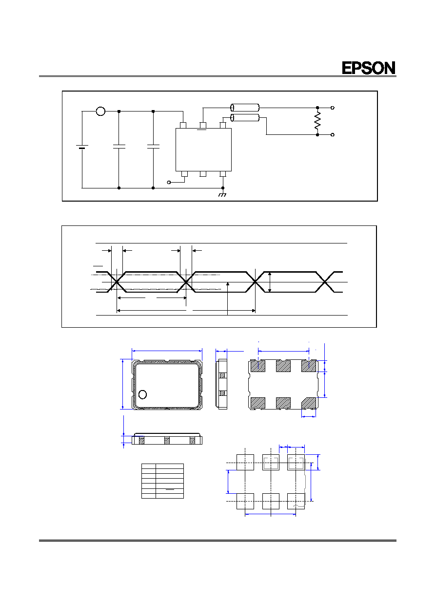
Generates high frequency clock from a high stability SAW (surface acoustic wave) resonator.
∑
2.5V-LVDS output.
∑
Very low jitter/low phase noise.
∑
Small SMD in 7x5mm, Max1.4mm height, ceramic package.
Applications
∑
Gigabit Ethernet, Fibre channel, Infini Band, PCI-express, Rapid IO, Hyper Transport, Memory clock, CPU clock
Absolute Maximum Ratings
Item Symbol
Unit
MIN.
TYP.
MAX. Condition
Supply Voltage
V
CC
V -0.5 +4.0
V
CC
≠ GND
Storage temperature
Tstg
∞
C
-40
+100
Stored as bare product
Solder heat resistance
Tsol
Max. 240
∞
C x Max. 10s x 2 times
Operating range
Item Symbol
Unit
MIN.
TYP.
MAX. Condition
Supply voltage
V
CC
V 2.375 2.5 2.625
0 +70
P
version
Operating temperature
Topr
∞
C
-5 +85
R
version
Output load
RL
100 Differential
resistor
Frequency characteristics (V
CC
=2.375 to 2.625,GND=0.0V,Load=100
)
Item
Symbol
Unit MIN. TYP. MAX.
Condition
Output frequency Range
fosc
MHz
53.125
700
-100
+100
H version, *1
Frequency Stability
df/f0
ppm
-50
+50
G version, *1
*1 This includes initial frequency tolerance, temperature, supply voltage variation and loading variation. Please refer to Part Numbering Guide (page3).
Electrical characteristics (V
CC
=2.375 to 2.625,GND=0.0V,Load=100
)
Item Symbol
Unit
MIN.
TYP.
MAX. Condition
Start up time
Tosc
ms
10
t=0 at V
CC
=2.375V
20
30
fosc<=500MHz
Current consumption
I
OP
mA
25
35
fosc>500MHz
OE High level input voltage
V
IH
V 0.7V
CC
OE Low level input voltage
V
IL
V
0.3V
CC
OE High level input current
I
IH
uA
1
OE=
V
CC
OE Low level input current
I
IL
uA -100
-10
OE=GND
Differential output voltage
V
OD
mV 247 350 454
V
OD1
,V
OD2
Change to V
OD
dV
OD
mV
50 dV
OD
=
V
OD1
- V
OD2
Offset Voltage
V
OS
V 1.125 1.25 1.375
V
OS1
,V
OS2
Change to V
OS
dV
OS
mV
150 dV
OS
=
V
OS1
- V
OS2
48
52
V version: <=175MHz
45
55
53.125M to 350MHz
Duty
at outputs crossing point
tw/t %
40 60
>350M
Output Rise time
t
TLH
ps
400
20-80% of V
OD
Output Fall time
t
THL
ps
400
80-20% of V
OD
UI
0.044x10
-3
53.125 to 700MHz
Phase Jitter *2
Offset =12KHz to 20MHz
T
PJ
ps 0.29 1
@156.25MHz
t
RJ
ps
3
4
of Random Jitter
Period Jitter *3
n=50000 samples
t
p-p
ps
25
40
Peak to Peak of jitter distribution
Accumulated Jitter *3
n=2 to 50000 cycles
t
acc
ps
4
5
of Total jitter distribution
*2 Measured by SSB phase noise test equipment.
*3 Measured by Time interval analyzer or oscilloscope.
EPSON ELECTRONICS AMERICA, INC.
www.eea.epson.com
EG2121 LVDS Rev 1.4 35D
Part Numbering Guide
*1 Available combination : xHPA, xHPN, xHRA, xHRN, xGPN
For xGPA and xGRN stability, please contact Epson.
xGRA is not available.
*2 V (Duty +/-2%) version is available under 175MHz.
Standard Frequency List
53.1250 *3
62.5000 *3
100.0000 106.2500 125.0000 133.0000
155.5200 156.2500
159.3750
161.1328 *4
200.0000
212.5000
250.0000
311.0400
312.5000
322.2656 *5
400.0000
425.0000
500.0000
622.0800
625.0000
644.5313 *6
Please round off 5
th
digit and specify 4-digit accuracy under decimal point.
*3 available only xHPA and xHPN.
Nominal frequency: *4=161.1328125MHz, *5=322.265625MHz, *6=644.53125MHz
EPSON ELECTRONICS AMERICA, INC.
www.eea.epson.com
EG-2121CA - 156.2500M - L H P A
Stability condition A: Including 10yrs Aging N: Excluding Aging
Temperature Range P: 0 to +70C R: - 5 to +85C
Frequency Stability H: +/-100ppm G: +/-50ppm
Output L: LVDS V: LVDS (Duty +/-2%)*2
Output Frequency : see Standard frequency list