GRAPHICS
SED1353
X18A-C-001-08
1
October 1998
SED1353 GRAPHICS LCD CONTROLLER
s
DESCRIPTION
The SED1353 is a dot matrix graphic LCD controller supporting resolutions up to 1024x1024. It is
capable of displaying a maximum of 256 simultaneous colors out of a possible 4096 or 16 gray shades.
Design flexibility allows the SED1353 to interface to either an MC68000 family microprocessor or an
8/16-bit MPU/bus with minimum external logic. The Static RAM (SRAM) interface used for the display buffer
is optimized for speed and performance, supporting up to 128K bytes.
Two power save modes, combined with operating voltages of 2.7 volts through 5.5 volts, allow for a wide
range of applications while providing minimum power consumption.
s
FEATURES
�
pin compatible with the SED1352
�
16-bit 16 MHz MC68xxx MPU interface
�
8/16-bit MPU interface controlled by a READY
(or WAIT#) signal
�
option to use built-in index register or direct-map-
ping to access one of sixteen internal registers
�
2-terminal crystal or external oscillator support
�
8/16-bit SRAM interface configurations
�
split screen display support allowing two different
images to be simultaneously displayed
�
virtual display support (displays images larger
than the panel size through the use of panning)
�
display modes:
black-and-white display
2/4 bits per pixel, 4/16-level gray-scale display
2/4/8 bits per pixel, 4/16/256-level color display
�
two software power-save modes
�
low power consumption
�
display memory interface:
128K bytes using one 64Kx16 SRAMs
128K bytes using two 64Kx8 SRAMs
64K bytes using two 32Kx8 SRAMs
40K bytes using one 8Kx8 and one 32Kx8
SRAM
32K bytes using one 32Kx8 SRAM
16K bytes using two 8Kx8 SRAMs
8K bytes using one 8Kx8 SRAM
�
LCD panel configurations:
single-panel, single-drive passive display
dual-panel, dual-drive passive display
�
maximum number of vertical lines:
1,024 lines (single-panel, single-drive display)
2,048 lines (dual-panel, dual-drive display)
�
QFP5-100-S2 package (F0A)
�
QFP15-100-STD package (F1A)
s
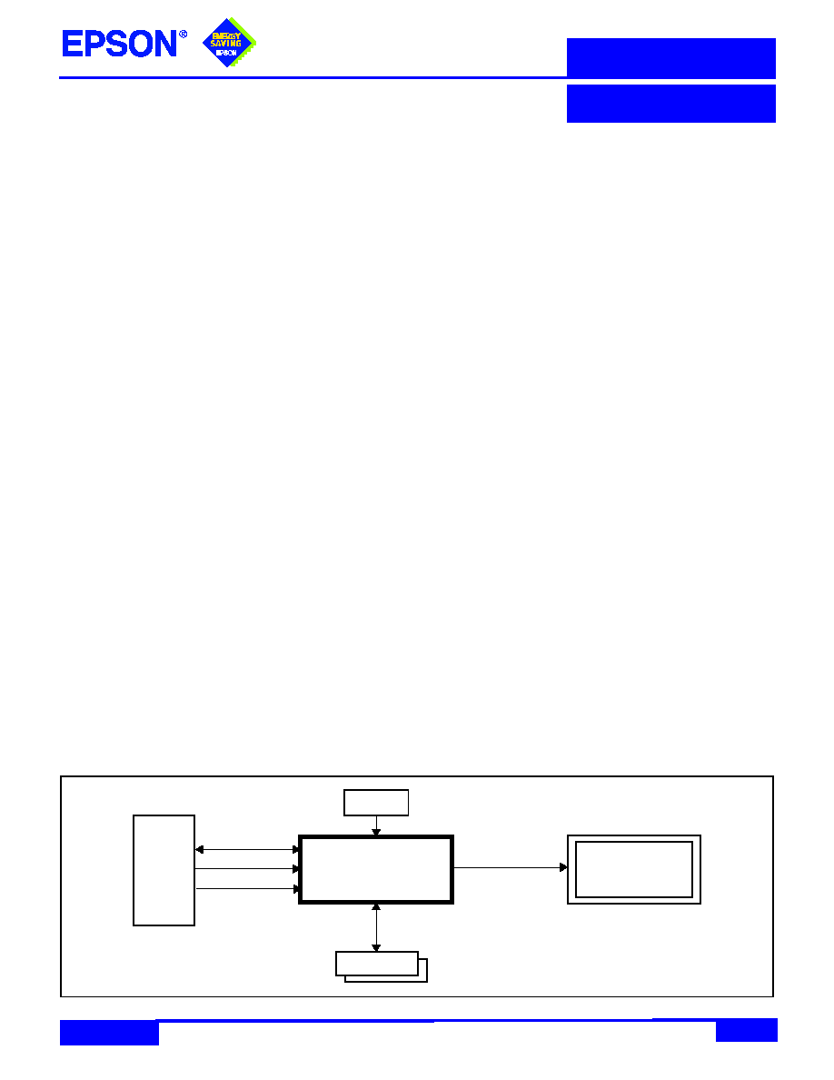
SYSTEM BLOCK DIAGRAM
LCD PANEL
MPU
SED1353
SRAM
CLOCK
80xx
Z80
68xxx
DATA
CONTROL
ADDRESS
GRAPHICS
SED1353
X18A-C-001-08
2
s
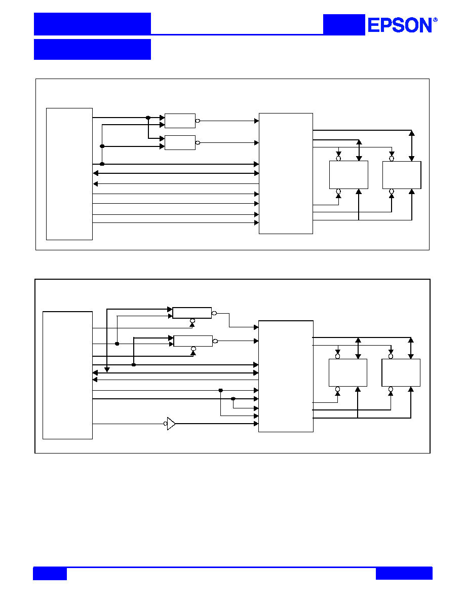
INTERFACE OPTIONS
Note: Example implementation, actual may vary.
Note: Example implementation, actual may vary.
SED1353
MEMCS#
IOCS#
MC68xxx
DTACK#
D0 to D15
A1 to A19
AB1 to AB19
DB0 to DB15
IOW#
IOR#
Decoder
AS#
R/W#
BHE#
UDS#
READY
A20 to A23
AB0
LDS#
Decoder
A14 to A16
A10 to A19
FC0 to FC1
Interface with 16-Bit MC68xxx MPU and 16K bytes SRAM (2 of 8K x 8)
64 Kbit
VWE#
VD0-7
VCS0#
VCS1#
VA0-12
WE#
CS#
64 Kbit
WE#
CS#
VD8-15
MEMCS#
MEMW#
MEMR#
READY
DB0 to DB7
AB0 to AB15
IOCS#
IOW#
IOR#
RESET
SED1353
Z80
RESET#
D0 to D7
WAIT#
A0 to A15
WR#
RD#
Decoder
IORQ#
A10 to A15
Decoder
MREQ#
Interface with 8-Bit Z80 MPU and 16K bytes SRAM (2 of 8K x 8)
64 Kbit
VWE#
VD0-7
VCS0#
VCS1#
VA0-12
WE#
CS#
64 Kbit
WE#
CS#
MI#
GRAPHICS
SED1353
X18A-C-001-08
3
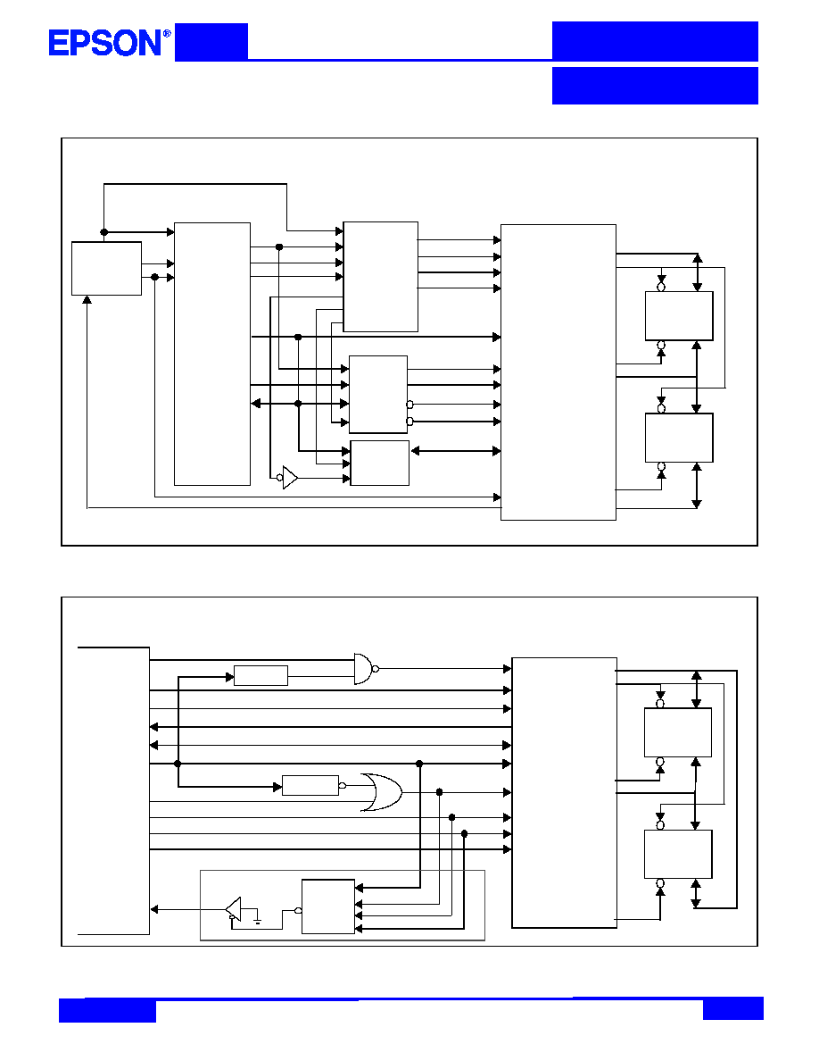
Note: Example implementation, actual may vary.
Note: Example implementation, actual may vary.
8086
(Maximum mode)
CLK
READY
RESET#
RDY
MEMW#
MEMR#
READY
DB0 to DB15
AB0 to AB15
IOW#
IOR#
RESET
SED1353
8284A
D0 to D15
T
OE
CLK
S2#
S1#
S0#
DEN
MRDC#
AMWC#
IORC#
AIOWC#
DT/R
CLK
READY
RESET#
8288
AB16 to AB19
M/IO#
BHE#
A0 to A16
STB
Decoder
A16 to A19
S2#
S1#
S0#
ALE
BHE#
AD0 to AD15
A16
BHE#
MEMCS#
IOCS#
Interface with 16-Bit 8086 MPU and 64K bytes SRAM (2 of 32K x 8)
256 Kbit
VWE#
VD0-7
VCS0#
VCS1#
VA0-14
WE#
CS#
256 Kbit
WE#
CS#
VD8-15
Transceiver
Interface with 8-Bit ISA Bus and 40K bytes SRAM (1 of 8K x 8 and 1 of 32K x 8)
SED1353
MEMCS#
MEMW#
MEMR#
READY
8-Bit ISA Bus
SMEMW#
SMEMR#
IOCHRDY
REFRESH
SA0 to SA19
SD0 to SD7
DB0 to DB7
AB0 to AB19
Decoder
SA13 to SA16
IOCS#
IOW#
IOR#
RESET
RESET#
SA10 to SA15
AEN
IOW#
IOR#
Decoder
0WS#
optional
SA(1 or 4) to SA9
Decoder
64 Kbit
VWE#
VD0-7
VCS0#
VCS1#
VA0-14
WE#
CS#
256 Kbit
WE#
CS#
GRAPHICS
SED1353
X18A-C-001-08
4
Note: Example implementation, actual may vary.
s
SUPPORTED RESOLUTIONS
The above listed display sizes are examples based on bits/pixel and available memory.
a. 256 colors must use 16-bit SRAM interface
Display
RAM
Example Display Size
SRAM
Type
CPU
Interface
SRAM
Interface
Monochrome
4 Grays/
Colors
16 Grays/
Colors
256 Colors
a
X Y
X Y
X Y
X Y
8K byte
320 x 200
256 x 128
128 x 128
--
1 of 8Kx8
8-bit
8-bit
16K byte
512 x 256
320 x 200
200 x 160
160 x 100
a
2 of 8Kx8
8-bit
8-bit/16-bit
16-bit
16-bit
32K byte
512 x 512
512 x 256
256 x 256
192 x 100
a
1 of 32Kx8
8-bit
8-bit
40K byte
1024 x 320
512 x 320
320 x 256
320 x 128
a
1 of 8Kx8 and
1 of 32Kx8
8-bit
8-bit
64K byte
1024 x 512
512 x 512
512 x 256
256 x 256
a
2 of 32Kx8
8-bit
8-bit/16-bit
16-bit
16-bit
128K byte
1024 x 1024
1024 x 512
512 x 512
512 x 256
a
1 of 64Kx16
16-bit
16-bit
2 of 64Kx8
16-bit
16-bit
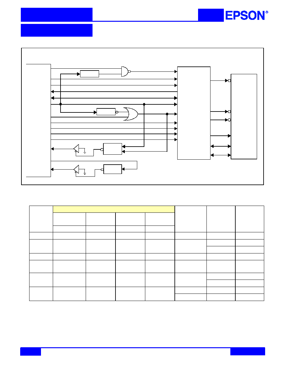
Interface with 16-Bit ISA Bus and 128K bytes SRAM (1 of 128K x 8)
SED1353
MEMCS#
MEMW#
MEMR#
READY
16-bit ISA Bus
SMEMW#
SMEMR#
IOCHRDY
REFRESH
SA0 to SA19
SD0 to SD15
DB0 to DB15
AB0 to AB19
Decoder
IOCS#
IOW#
IOR#
RESET
RESET#
Decoder
SA10 to SA15
AEN
IOW#
IOR#
IOCS16#
SA(1 or 4) to SA9
BHE#
SBHE#
Decoder
MEMCS16#
LA17 to LA23
SA14 to SA16
Decoder
VWE#
VD0-7
VD8-15
VCS0#
VCS1#
VA0-15
1 Mbit
WE#
UB#
LB#
A0-15
I/O 1-8
I/O 9-16
GRAPHICS
SED1353
X18A-C-001-08
5
s
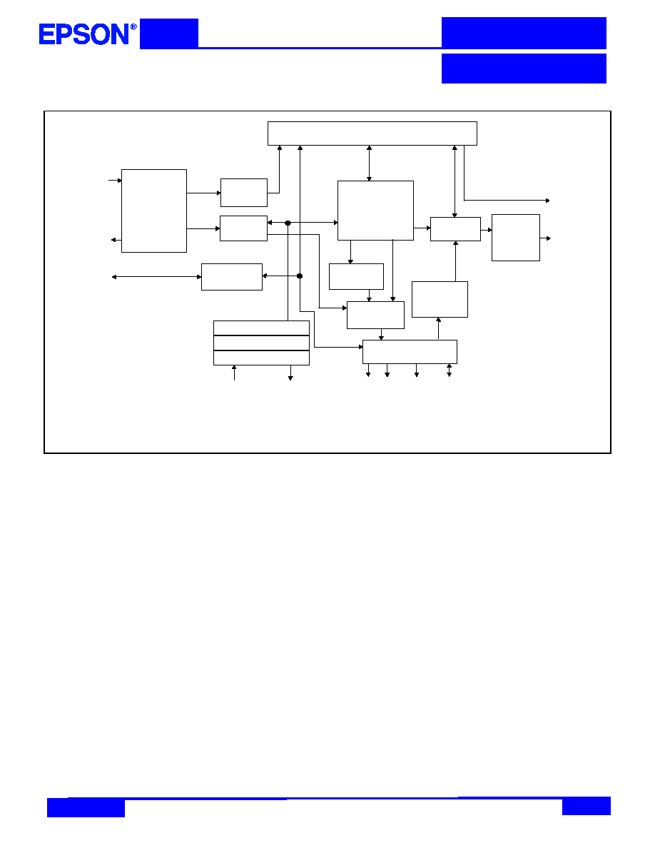
BLOCK DIAGRAM
Bus
Control Registers
Signal
Translation
Port
Memory
Data Bus
Timing Generator
Sequence
Address
MPU/CRT
SRAM Interface
Lookup
LCD
Decoder
Decoder
Conversion
Oscillator
Power Save
Selector
Display
Data
Formatter
Generator
Table
Controller
Panel
Interface
LCDENB
UD[3:0]
LD[3:0]
LP, YD,
XSCL,
OS
C1
OS
C2
VWE#
VOE#
VA
[
15:
0
]
VSC0
#
,
VSC1
#
VD[1
5
:0
]
IOR#, IOW#, IOCS#,
MEMCS#, MEMR#,
MEMW#, BHE#,
AB[19:0]
READY
DB[15:0]
WF(XSCL2)