67
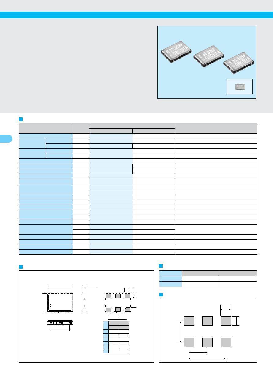
Crystal oscillator
Recommended soldering pattern
(Unit: mm)
External dimensions
Specifications (characteristics)
(Unit: mm)
DRC / DRH
GRC / GRH
±
35 x 10
-6
±
50 x 10
-6
Stability
-20
∞
C to +70
∞
C
-40
∞
C to +85
∞
C
Temperature range
1 V
C
2 NC OE
3 GND
4 OUT
5 OE NC
6 V
DD
NO.
F TYPE T TYPE
Pin terminal
5.08
1.5 Max.
5.08
1.4
5.0
±
0.2
#4
#5
#3
#2
#6
#4
#5
#6
#1
#3
#2
#1
2.54
2.6
1.1
E 35.328F
GRC181A
7.0
±
0.2
5.08
2.54
1.6
1.5
3.9
Stability / Temperature range
VOLTAGE-CONTROLLED CRYSTAL OSCILLATOR
VG-4231CA
∑ High accuracy and high reliability due to trimmerless design.
∑ Well designed internal construction realizes as good as general
- purpose ICs heat resistance performance.
∑ Use of CMOS IC assures low current consumption.
∑ Excellent shock resistance and environmental capability.
∑ Supply voltage: 5.0 V(DRH / GRH),3.3 V(DRC / GRC)
∑ Output enable function(OE) can be used for low current
consumption applications.
Item
Output frequency range
Power source
voltage
Temperature
range
Frequency stability
Current consumption
Output disable current
Pull range
Modulation Characteristics
Absolute pull range
Input resistance
Frequency change polarity
Duty
Output voltage
Output load condition (fan out)
Output enable/
disable input voltage
Output rise time
Output fall time
Oscillation start up time
Aging
Symbol
f
0
V
DD
-GND
V
DD
T
STG
T
OPR
f/f
0
lop
I
OE
f
C
BW
APR
Z
IN
t
W
/t
V
OH
V
OL
N/C
L
V
IH
V
IL
t
TLH
t
THL
t
OSC
fa
Specifications
DRH / GRH
DRC / GRC
16.0000 MHz to 41.0000 MHz
-0.3 V to +7.0 V
H : 5.0 V ±0.5 V
C : 3.3 V ±0.3 V
-40 ∞C to +125 ∞C
As per below table
As per below table
20 mA Max.
10 mA Max.
15 mA Max.
7 mA Max.
R : ±130 x 10
-6
± 15 kHz Min.
D : ±80 x 10
-6
Min
G : ±65 x 10
-6
Min
50 k Min.
Positive polarity
40 % to 60 %
V
DD
-0.4 V Min.
0.4 V Max.
15 pF Max.
0.7 V
DD
Min.
0.3 V
DD
Max.
4 ns Max.
4 ns Max.
10 ms Max.
±10 x 10
-6
Max.
Remarks
Please contact us for inquiries about the available frequency.
Stored as bare product after unpacking
VC=2.5 V(DRH / GRH) / VC=1.65 V(DRC / GRC)
No load condition
OE=GND
VC=2.5±2.0 V(DRH / GRH) / VC=1.65±1.50 V(DRC / GRC)
± 3 dB at 1kHz
DC Level
1/2V
DD
level
I
OH
= -0.8 mA(DRC / GRC)/I
OH
= -4 mA(DRH / GRH)
I
OL
= 3.2 mA(DRC / GRC)/I
OL
= 4 mA(DRH / GRH)
CMOS load
OE terminal
CMOS load: 20
%
80
%
V
DD
level
CMOS load: 80
%
20
%
V
DD
level
Time at 0.9 V
DD
to be 0 s
Ta=+25 ∞C, 10 year
Max. supply voltage
Operating voltage
Storage temperature
Operating temperature
Actual size
Product number (please refer to page 2)
Q 3 6 1 4 C A 0 x x x x x 0 0