
February 1999
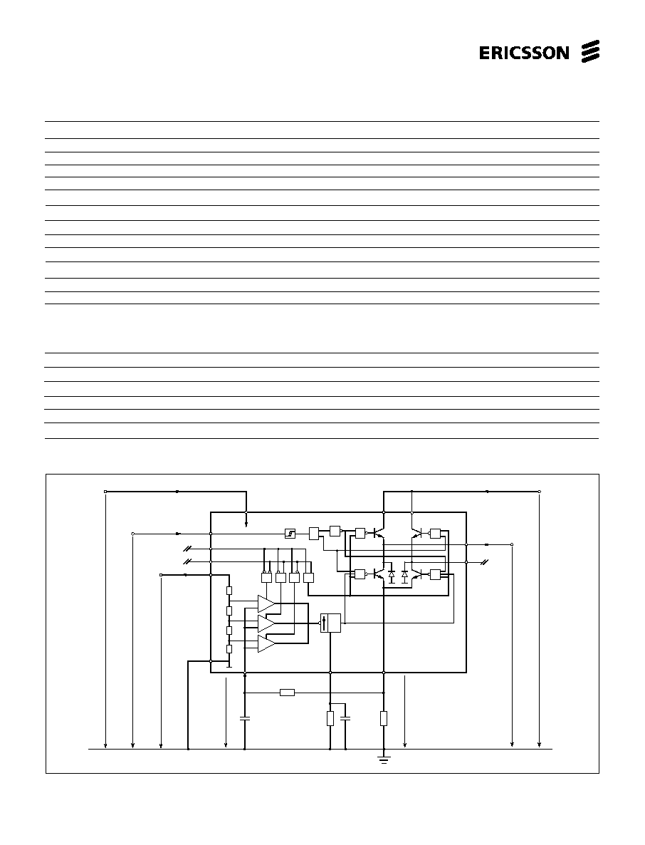
Figure 1. Block diagram.
PBL 3770A
High Performance
Stepper Motor Drive Circuit
PBL3770A
PBL
3770A
16-pin plastic batwing DIP
28-pin plastic PLCC package
20-pin SO
Description
PBL 3770A is a bipolar monolithic circuit intended to control and drive the current in
one winding of a stepper motor. It is a high power version of PBL 3717 and special
care has been taken to optimize the power handling capability without suffering in
reliability.
The circuit consists of a LS-TTL compatible logic input stage, a current sensor, a
monostable multivibrator and a high power H-bridge output stage. The circuit is
pin-compatible with the PBL 3717 industry-standard driver.
Two PBL 3770A and a small number of external components form a complete
control and drive unit for LS-TTL or microprocessor-controlled stepper motor
systems.
Key Features
∑
Half-step and full-step operation.
∑
Switched mode bipolar constant
current drive
∑
Wide range of current control
5 -1800 mA.
∑
Wide voltage range 10 - 45 V.
∑
Designed for unstabilized motor
supply voltage.
∑
Current levels can be selected in
steps or varied continuously.
∑
Thermal overload protection.
1
GND
V
CC
M
A
M
B
Phase
I
1
I
0
V
R
&
&
&
&
≠
+
≠
+
≠
+
Monostable
t = 0.69 ∑ R ∑ C
Current Sensor
Output Stage
off
T T
Schmitt
Trigger
Time
Delay
C
T
E
PBL 3770A
1
1
1
1
V
MM
V
MM
1
PBL 3770A
PBL 3770A
2
Maximum Ratings
Parameter
Pin no. [DIL package]
Symbol
Min
Max
Unit
Voltage
Logic supply
6
V
CC
0
7
V
Motor supply
3, 14
V
MM
0
45
V
Logic inputs
7,8,9
V
I
-0.3
6
V
Comparator input
10
V
C
-0.3
V
CC
V
Reference input
11
V
R
-0.3
15
V
Current
Motor output current
1, 15
I
M
-1800
+1800
mA
Logic inputs
7,8,9
I
I
-10
mA
Analog inputs
10,11
I
A
-10
mA
Temperature
Operating junction temperature
T
J
-40
+150
∞
C
Storage temperature
T
s
-55
+150
∞
C
Recommended Operating Conditions
Parameter
Symbol
Min
Typ
Max
Unit
Logic supply voltage
V
CC
4.75
5
5.25
V
Motor supply voltage
V
MM
10
40
V
Motor output current
I
M
-1500
+1500
mA
Junction temperature
T
J
-20
+125
∞
C
Rise time logic inputs
t
r
2
µ
s
Fall time logic inputs
t
f
2
µ
s
Figure 2. Definition of symbols.
V
CC
I I
M OL
I
CC
I I I
I IH IL
I
A
820 pF
0.5
V
CC
V
V
V
I
IH
IL
V
V
A
R
V
C
I
I
C
A
V
E
V
V
M
MA
V
MM
R
R
C
820 pF
C
1 k
S
T
T
C
R
C
56 k
M
A
M
B
C
V
I MM
GND
Phase
I
1
I
0
V
R
&
&
&
&
≠
+
≠
+
≠
+
Monostable
t = 0.69 ∑ R ∑ C
Current Sensor
Output Stage
off
T T
Schmitt
Trigger
Time
Delay
C
T
E
PBL 3770A
1
1
1
1
10
2
16
1
15
14
6 [18]
8
7
9
11
4, 5,
12, 13
3
V
MM
V
MM
1
Pin no. refers
to DIL-package

PBL 3770A
3
Electrical Characteristics
Electrical characteristics over recommended operating conditions. C
T
= 820 pF, R
T
= 56 kohm.
Ref.
Parameter
Symbol fig.
Conditions
Min
Typ
Max
Unit
General
Supply current
I
CC
2
V
MM
= 20 to 40 V, I
0
= I
1
= HIGH.
30
40
mA
V
MM
= 20 to 40 V, I
0
= I
1
= LOW,
48
65
mA
f
s
= 23 kHz
Total power dissipation
P
D
f
s
= 28 kHz, I
M
= 1000 mA, V
MM
= 36 V
1.9
2.3
W
Note 2, 4.
f
s
= 24 kHz, I
M
= 1000 mA, V
MM
= 12 V
1.7
2.1
W
Note 2, 4.
f
s
= 28 kHz, I
M
= 1300 mA, V
MM
= 36 V
2.7
3.2
W
Note 3, 4.
f
s
= 28 kHz, I
M
= 1500 mA, V
MM
= 36 V
3.5
W
Note 3, 4.
Turn-off delay
t
d
3
T
a
= +25
∞
C, dV
C
/dt
50 mV/
µ
s.
2.5
µ
s
Thermal shutdown junction temperature
170
∞
C
Logic Inputs
Logic HIGH input voltage
V
IH
2
2.0
V
Logic LOW input voltage
V
IL
2
0.8
V
Logic HIGH input current
I
IH
2
V
I
= 2.4 V
20
µ
A
Logic LOW input current
I
IL
2
V
I
= 0.4 V
-0.4
mA
Analog Inputs
Comparator threshold voltage
V
CH
2
V
R
= 5.0 V, I
0
= I
1
= LOW
400
415
430
mV
Comparator threshold voltage
V
CM
2
V
R
= 5.0 V, I
0
= HIGH, I
1
= LOW
240
250
265
mV
Comparator threshold voltage
V
CL
2
V
R
= 5.0 V, I
0
= LOW, I
1
= HIGH
70
80
90
mV
Input current
I
C
2
-20
µ
A
Motor Outputs
Lower transistor saturation voltage
I
M
= 1000 mA
0.5
0.8
V
I
M
= 1300 mA
0.8
1.3
V
Lower diode forward voltage drop
I
M
= 1000 mA
1.3
1.6
V
I
M
= 1300 mA
1.5
1.8
V
Upper transistor saturation voltage
I
M
= 1000 mA
1.1
1.3
V
I
M
= 1300 mA
1.3
1.6
V
Output leakage current
I
0
= I
1
= HIGH, T
a
= +25
∞
C
100
µ
A
Monostable
Cut off time
t
off
3
V
MM
= 10 V, t
on
5
µ
s
27
31
35
µ
s
Thermal Characteristics
Ref.
Parameter
Symbol Fig. Conditions
Min
Typ
Max
Unit
Thermal resistance
Rth
J-C
DIL package.
11
∞
C/W
Rth
J-A
15 DIL package. Note 2.
40
∞
C/W
Rth
J-C
PLCC package.
9
∞
C/W
Rth
J-A
15 PLCC package. Note 2.
35
∞
C/W
Rth
J-C
SO package.
11
∞
C/W
Rth
J-A
15 SO package.
40
∞
C/W
Notes
1.
All voltages are with respect to ground. Currents are positive into, negative out of specified terminal.
2.
All ground pins soldered onto a 20 cm
2
PCB copper area with free air convection. T
a
= +25
∞
C.
3.
DIP package with external heatsink (Staver V7) and minimal copper area. Typical Rth
J-A
= 27.5
∞
C/W. T
a
= +25
∞
C.
4.
Not covered by final test program.
PBL 3770A
4
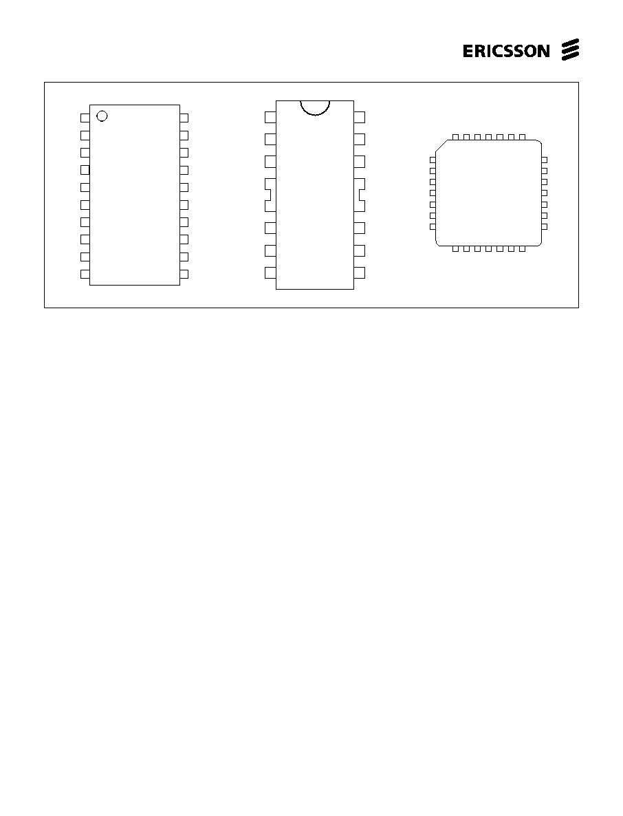
Figure 3. Pin configurations.
Pin Description
SO
DIP
PLCC
Symbol
Description
1
1
10
M
B
Motor output B, Motor current flows from M
A
to M
B
when Phase is high.
2
2
11
T
Clock oscillator. Timing pin connect a 56 k
resistor and a 820 pF in
parallel between T and Ground.
3
3,14
12,4
V
MM
Motor supply voltage, 10 to 40 V. Pin 3(12) and pin 14(4) should be wired together.
4-7,
4,5,
1-3,9,
GND
Ground and negative supply. Note these pins are used for heatsinking.
14-18
12,13
13-17,28
Make sure that all ground pins are soldered onto a suitable large copper
ground plane for efficient heat sinking.
8
6
18
V
CC
Logic voltage supply normally +5 V.
9
7
19
I
1
Logic input. It controls, together with the I0 input, the current level in the output stage.
The controlable levels are fixed to 100, 60, 20, 0%.
10
8
20
Phase
Controls the direction of the motor current of M
A
and M
B
outputs.
Motor current flows from M
A
to M
B
when the phase input is high.
11
9
21
I
0
Logic input. It controls, together with the I1 input, the current level in the output stage.
The controlable levels are fixed to 100, 60, 20, 0%.
12
10
23
C
Comparator input. This input senses the instaneous voltage across the sensing
resistor, filtered through a RC Network.
13
11
24
V
R
Reference voltage. Controls the threshold voltage of the comparator and hence
the output current. Input resistance: typically 6.8 k
±
20%.
19
15
6
M
A
Motor output A, Motor current flows from M
A
to M
B
when Phase is high.
20
16
8
E
Common emitter. Connect the Sence resistor between this pin and ground.
1
2
3
4
5
6
7
8
9
10
18
17
16
15
14
13
12
11
I1
VR
M
B
VCC
T
VMM
GDN
E
Phase
0
C
19
20
GDN
GDN
GDN
GDN
GDN
GDN
GDN
VMM
M
A
PBL
3770A
I
B
T
MM
GND
GND
CC
1
Phase
E
M
GND
GND
V
C
I
1
2
3
4
5
6
7
8
16
15
14
13
12
11
10
9
A
V
MM
R
0
I
V
V
M
PBL
3770A
N/C
A
N/C
E
GND
B
T
N/C
V
C
N/C
I
Phase
I
V
GND
GND
GND
GND
N/C
N/C
MM
GND
GND
GND
GND
GND
CC
5
6
7
8
9
10
11
25
24
23
22
21
20
19
4
3
2
1
28
27
26
12
13
14
15
16
17
18
MM
R
0
1
V
V
M
M
PBL
3770A

PBL 3770A
5
Functional Description
The PBL 3770A is intended to drive a
bipolar constant current through one
winding of a 2-phase stepper motor.
Current control is achieved through
switched-mode regulation, see figure 5
and 6.
Three different current levels and zero
current can be selected by the input
logic.
The circuit contains the following
functional blocks:
∑
Input logic
∑
Current sense
∑
Single-pulse generator
∑
Output stage
Input logic
Phase input. The phase input
determines the direction of the current in
the motor winding. High input forces the
current from terminal M
A
to M
B
and low
input from terminal M
B
to M
A
. A Schmitt
trigger provides noise immunity and a
delay circuit eliminates the risk of cross
conduction in the output stage during a
phase shift.
Half- and full-step operation is
possible.
Current level selection. The status of I
0
and I
1
inputs determines the current level
in the motor winding. Three fixed current
levels can be selected according to the
table below.
Motor current
I
0
I
1
High level
100%
L
L
Medium level
60%
H
L
Low level
20%
L
H
Zero current
0%
H
H
The specific values of the different
current levels are determined by the
reference voltage V
R
together with the
value of the sensing resistor R
S
.
The peak motor current can be
calculated as follows:
i
m
= (V
R
∑ 0.080) / R
S
[A], at 100% level
The motor current can also be
continuously varied by modulating the
voltage reference input.
Current sensor
The current sensor contains a reference
voltage divider and three comparators
for measuring each of the selectable
current levels. The motor current is
sensed as a voltage drop across the
current sensing resistor, R
S
, and
compared with one of the voltage
references from the divider. When the
two voltages are equal, the compara-tor
triggers the single-pulse generator. Only
one comparator at a time is activa-ted by
the input logic.
Single-pulse generator
The pulse generator is a monostable
multivibrator triggered on the positive
edge of the comparator output. The
multivibrator output is high during the
pulse time, t
off
, which is determined by
the timing components R
T
and C
T
.
t
off
= 0.69 ∑ R
T
∑ C
T
The single pulse switches off the
power feed to the motor winding,
causing the winding to decrease during
t
off
.
If a new trigger signal should occur
during t
off
, it is ignored.
Output stage
The output stage contains four
transistors and two diodes, connected in
an H-bridge. Note that the upper
recirculation diodes are connected to the
circuit externally. The two sinking
transistors are used to switch the power
supplied to the motor winding, thus
driving a constant current through the
winding. See figures 5 and 6.
Overload protection
The circuit is equipped with a thermal
shut-down function, which will limit the
junction temperature. The output current
will be reduced if the maximum permis-
sible junction temperature is exceeded.
It should be noted, however, that it is not
short circuit protected.
Operation
When a voltage V
MM
is applied across
the motor winding, the current rise
follows the equation:
i
m
= (V
MM
/ R) ∑ (1 - e
-(R ∑ t ) / L
)
R = Winding resistance
L = Winding inductance
t
= time
(see figure 6, arrow 1)
The motor current appears across the
external sensing resistor, R
S
, as an
analog voltage. This voltage is fed
through a low-pass filter, R
C
C
C
, to the
voltage comparator input (pin 10). At the
moment the sensed voltage rises above
the comparator threshold voltage, the
monostable is triggered and its output
turns off the conducting sink transistor.
The polarity across the motor winding
reverses and the current is forced to
circulate through the appropriate upper
protection diode back through the source
transistor (see figure 6, arrow 2).
After the monostable has timed out,
the current has decayed and the analog
Figure 4. Definition of terms.
| V ≠ V |
1/2
1
V
CH
t
on
t
off
f =
s
t
on
t
off
+
Normalized
V
E
MA
MB
t
d
t
t
V
CM
V
CL
D =
t
on
t
off
+
1
t
on