 | –≠–ª–µ–∫—Ç—Ä–æ–Ω–Ω—ã–π –∫–æ–º–ø–æ–Ω–µ–Ω—Ç: PKG4627PI | –°–∫–∞—á–∞—Ç—å:  PDF PDF  ZIP ZIP |

∑ Efficiency typ 86% (5 V) at full load
∑ Low profile 11.0 mm (0.43 in.)
∑ 1,500 V dc isolation voltage
(duals = 1,000 Vdc)
∑ MTBF >200 years at +75∞C case
temperature
∑ Rugged mechanical design and
efficient thermal management, max
+100 ∞C case temperature
∑ EMI measured according to
EN 55 022 and FCC part 15J
The PKG series of DC/DC Power Modules are mem-
bers of the EriPowerTM range of low profile DC/DC
converters for distributed power architectures in
48/60 VDC power systems. They provide up to 60W
in single and dual output versions. Utilizing the
standard EriPowerTM PKA/PKE pin-out with an even
smaller footprint, the power density is 20 W/cu.in.
The PKG units can be used as on-board distributed
power modules, or serve as building blocks for more
centralized power boards. The high efficiency makes it
possible to operate over a wide temperature range
without any extra heatsinks. At forced convection
cooling >200 lfm (1 m/s), the PKG units can deliver
full power without heatsinks up to +65∞C ambient.
With derated output power it can also operate in
E
PKG 4000 I
30≠60 W DC/DC Power Modules
48 V Input Series
temperature controlled environments with non-forced
convection cooling. By adding external heatsinking,
the temperature range can be extended even further.
Thanks to its peak power capa-bility, the PKG series
is ideal for applications where max power is only
required during short durations e.g. in disc drives.
The PKG series uses ceramic sub-strates with plated
copper in order to achieve good thermal manage-
ment, low voltage drops, and a high efficiency.
These products are manufactured using highly
automated manufacturing lines with a world-class
quality commitment and a five-year warranty.
Ericsson Microelectronics AB has been an ISO 9001
certified supplier since 1991. For a complete product
program please reference the back cover.

2
EN/LZT 146 04 R1B © Ericsson Microelectronics, November 2001
General
Safety
The PKG 4000 I Series DC/DC power mod-
ules are designed in accordance with EN 60
950 Safety of information technology equipment
including electrical business equipment and certi-
fied by SEMKO. The isolation is an opera-
tional insulation in accordance with EN
60 950.
The PKG DC/DC power modules are re-
cognized by UL and meet the applicable
requirements in UL 1950 Safety of information
technology equipment, the applicable Canadian
safety requirements and UL 1012 Standard for
power supplies.
The DC/DC power module shall be installed
in an end-use equipment and is intended to
be supplied by isolated secondary circuitry
and shall be installed in compliance with the
requirements of the ultimate application.
When the supply to the DC/DC power
module meets all the requirements for SELV
(<60Vdc), the output is considered to remain
within SELV limits (level 3). If connected to a
60 V DC power system reinforced insulation
must be provided in the power supply that
isolates the input from the ac mains. Single
fault testing in the power supply must be
performed in combination with the DC/DC
power module to demonstrate that the output
meets the requirement for SELV. One pole of
the input and one pole of the output is to be
grounded or both are to be kept floating.
The terminal pins are only intended for con-
nection to mating connectors of internal
wiring inside the end-use equipment.
These DC/DC power modules may be used in
telephone equipment in accordance with
paragraph 34 A.1 of UL 1459 (Standard for
Telephone Equipment, second edition).
The isolation voltage is a galvanic isolation
and is verified in an electric strength test.
Test voltage between input and output and
between case and output is 1,500 V dc
(duals =1,000 V dc) for 60 s. In production
the test duration may be decreased to 1 s.
The capacitor between input and output has a
value of 4.7 nF (duals = 22 nF) and the leak-
age current is less than 1
m
A @ 50 Vdc.
Flammability ratings of the terminal support
and internal plastic construction details
meets UL 94V-0.
Absolute Maximum Ratings
Stress in excess of Absolute Maximum Ratings may cause permanent damage. Absolute Maximum Ratings, sometimes
referred to as no destruction limits, are normally tested with one parameter at a time exceeding the limits of Output data or
Electrical Characteristics. If exposed to stress above these limits, function and performance may degrade in an unspecified
manner.
Characteristics
min
max
Unit
T
C
Case temperature @ max output power
≠ 45
+100
∞C
T
S
Storage temperature
≠ 55
+125
∞C
V
I
Input voltage
≠ 0.5
+ 80
V dc
Isolation voltage
single output
1,500
(input to output test voltage) dual output
1,000
V dc
V
ISO
V
RC
Remote control voltage pin 1
≠ 10
+ 10
V dc
V
adj
Output adjust voltage pin 10
≠ 10
+ 10
V dc
Input T
C
< T
C max
Characteristics
Conditions
min
typ
max
Unit
V
I
Input voltage range
1)
38
72
V
V
Ioff
Turn-off input voltage
(See Operating Information)
32
V
V
Ion
Turn-on input voltage
(See Operating Information)
33
V
C
I
Input capacitance
1.8
mF
I
O
=0,T
C
= ≠30...+90∞C
1.5
2.0
W
Equivalent inrush
current resistance
m
W
r
Irush
Input idling power
P
Ii
Input stand-by current
V
I
= 53 V, T
C
= +25 ∞C
RC connected to pin 4
P
RC
1.0
W
30
Characteristics
Frequency
10...500 Hz
Amplitude
0.75 mm
Acceleration
10 g
Number of cycles
10 in each axis
Vibration
(Sinusoidal)
IEC 68-2-6 F
c
Test procedure & conditions
Environmental Characteristics
Frequency
10...500 Hz
Acceleration density
spectrum
0.5 g
2
/Hz
Duration
10 min in 3 directions
Reproducability
medium (IEC 62-2-36)
IEC 68-2-34 E
d
Random
vibration
Peak acceleration
200 g
Shock duration
3 ms
Shock
(Half sinus)
IEC 68-2-27 E
a
Temperature
≠40∞C...+125∞C
Number of cycles
100
Temperature
change
IEC 68-2-14 N
a
Temperature, solder
260∞C
Duration
10...13 s
Accelerated
damp heat
Solder
resistability
IEC 68-2-3 C
a
with bias
IEC 68-2-20 T
b
1A
Temperature
85∞C
Humidity
85% RH
Duration
1000 hours
Water
+55 ±5∞C
Isopropyl alcohol
+35 ±5∞C
Terpens
+35 ±5∞C
Method
with rubbing
Resistance to
cleaning solvents
IEC 68-2-45 XA
Method 1
Note:
The input voltage range 38...72 V meets the
requirements in the European Telecom Standard
prETS 300 132-2 for Normal input voltage
range in 48 V and 60 V DC power systems,
≠40.5...≠57.0 V and ≠50.0...≠72.0 V
respectively. At input voltages exceeding 72 V
(abnormal voltage) the power loss will be higher
than at normal input voltage and T
C
must be
limited to max +90 ∞C. Absolute max con-
tinuous input voltage is 80 V dc. Output
characteristics will be marginally affected at
input voltages exceeding 72 V.
1)
3
EN/LZT 146 04 R1B © Ericsson Microelectronics, November 2001
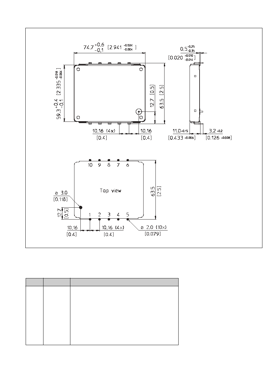
Mechanical Data
Dimensions in mm (in)
Foot print Component side
Case
Blue anodized aluminium casing with em-
bedded tin plated copper pins.
Weight
Maximum 75 g (2.66 oz).
Pin
Designation
Function
Connections
1
RC
Remote control. To turn-on and turn-off the output and to set the
turn-off input voltage threshold.
2
TOA
Turn-off input voltage adjust (see Operating information).
3
+In
Positive input. Connected to case.
4
≠ In
Negative input.
5
NC
Not connected.
6
≠ Out 2
Negative output 2.
7
+Out 2
Positive output 2.
8
≠ Out 1
Negative output 1.
9
+Out 1
Positive output 1.
10
V
adj
Output voltage adjust.

4
EN/LZT 146 04 R1B © Ericsson Microelectronics, November 2001
Thermal Data
Two-parameter model
Power dissipation is generated in the components mounted on the
ceramic substrate. The thermal properties of the PKG power module is
determined by thermal conduction in the connected pins and thermal
convection from the substrate via the case.
The two-parameter model characterizes the thermal properties of the
PKG power module and the equation below can be used for thermal
design purposes if detailed information is needed. The values are given
for a module mounted on a printed board assembly (PBA).
Note that the thermal resistance between the substrate and the air,
R
th sub-A
is strongly dependent on the air velocity.
T
sub
= P
d
◊ R
th sub-P
◊ R
th sub-A
/(R
th sub-P
+ R
th sub-A
) + (T
P
≠T
A
)
◊ R
th sub-A
/(R
th sub-P
+ R
th sub-A
) + T
A
Where:
P
d
: dissipated power, calculated as P
O
◊ (1/
h
-1)
T
sub
: max average substrate temperature,
ª T
C
max
T
A
: ambient air temperature at the lower side of the power
module
T
P
: average pin temperature at the PB solder joint
R
th sub-P
: thermal resistance from T
sub
to the pins
R
th sub-A
: thermal resistance from T
sub
to T
A
v
: velocity of ambient air.
Air velocity in free convection is 0.2≠ 0.3 m/s (40-60 lfm).
Over Temperature Protection (OTP)
The PKG DC/DC power modules have an internal over temperature
protection circuit. If the case temperature exceeds min +115 ∞C the
power module will go in to OTP-mode. As long as the case
temperature exceeds min +115 ∞C the power module will operate in
OTP-mode.
During OTP-mode the output voltage pulsates between zero and
nominal output voltage, which reduces the power loss inside the power
module. The PKG DC/DC power module will automatically resume
normal operation when the temperature decreases below
min +115 ∞C.
T
sub
R
th sub-A
R
th sub-P
T
A
T
P
P
d
R
th sub-P
T
sub
R
th sub-A
v
T
A
T
P
10
15
20
0
5
0
2
6
4
Air velocity (m/s)
R
(
C/W)
th
sub-A
∞
R
= 2.5 C/W
th sub-P
∞
Single output
Fundamental circuit diagrams
Electrical Data
3
2
1
4
Case
Control
Isolated feedback
9
8
10
Dual output

5
EN/LZT 146 04 R1B © Ericsson Microelectronics, November 2001
0
14.5
A
PKG 4310 PI
Characteristics
Conditions
Output 1
min
typ
max
Unit
Output voltage initial
setting and accuracy
T
C
= +25 ∞C, I
O
= 14.5 A, V
I
= 53 V
V
Oi
Output voltage
tolerance band
V
O
Idling voltage
I
O
= 0 A
Load regulation
I
O
= 0.1 ...1.0
¥ I
O max
, V
I
= 53 V
t
tr
Load transient voltage
V
tr
Temperature coefficient
2)
T
coeff
Ramp-up time
t
r
Start-up time
t
s
0.1 ...0.9
¥ V
O
From V
I
connection
to V
O
= 0.9
¥ V
Oi
Output current
I
O
Max output power
3)
P
O max
Current limiting
threshold
I
lim
T
C
< T
C max
Short circuit current
I
sc
V
O
= 0.2 ... 0.5 V, T
A
= 25 ∞C
Output ripple
20 Hz ...5 MHz
Supply voltage
rejection (ac)
SVR
f = 100 Hz sine wave, 1 V
p-p
, V
I
= 53 V
(SVR = 20 log (1 V
p-p
/V
O p-p
))
Line regulation
I
O
= I
O max
Load transient
recovery time
2.07
2.10
2.13
V
3.5
V
mV
30
mV
+130
mV
≠ 210
mV
T
C
= ≠30...+90∞C, V
I
= 38 ...72V unless otherwise specified.
I
O
=I
O max
, T
C
<T
C max
see PKG 4310 PI Temperature characteristics
10
ms
30
ms
30
W
16.2
A
18
A
60
100
mV
p-p
V
O ac
56
dB
100
m
s
I
O
=I
O max
Long term drift
included
Output
I
O
= 0.1 ...1.0
¥ I
O max
V
I
= 38...60 V
V
I
= 50...72 V
2
2
Output adjust range
1)
1.90
2.30
V
I
O
=0.1 ... 1.0
¥ I
O max
, V
I
= 53 V
load step = 0.5◊ I
Omax
I
O
=
0.1...1.0
¥ I
O max
V
I
= 53 V
OVP
Over voltage protection
2.6
V
2.03
2.17
V
1)
See Operating information.
2)
Temperature coefficient is positive at low temperatures and negative at high temperatures.
3)
See also Typical Characteristics, Power derating.
Characteristics
Conditions
Unit
min
typ
max
Efficiency
h
Power dissipation
P
d
Miscellaneous
75
%
10
W
I
O
= I
O max
, V
I
= 53 V
I
O
= I
O max
, V
I
= 53 V
I
O
> 0.1 ◊ I
O max
Calculated value