
Key Features
∑ Industry standard Half-brick
58x61x8.5 mm (2.3x2.4x0.33 in)
∑ Low profi le, max 8.5 mm (0.33 in)
∑ Design for environment in a cost
effi cient open-frame design
∑ High effi ciency, typ. 93 % at 3.3 Vout
half load
∑ 1500 VDC input to output isolation,
meets isolation requirements equivalent
to Basic Insulation according to
IEC/EN/UL 60950
∑ More than 6 million hours predicted
MTBF at 55∞ C ambient and 1 m/s
(200 lfm) airfl ow
DC/DC converter
Input 36-75 Vdc
Output up to 30A/100W
PKJ 4000E PI
E
The PKJ 4000E series of high efficiency DC/DC
converters are designed to provide high quality on-board
power solutions in distributed power architectures used
in Internetworking equipment in wireless and wired
communications applications.
The PKJ 4000E series has industry standard half brick
footprint and pin-out and is only 8.5 mm (0.33 in)
high. This makes it extremely well suited for narrow
board pitch applications with board spacing down to
15 mm (0.6 in). The PKJ 4000E series uses patented
synchronous rectification technology and achieves
an efficiency up to 89% at full load. Ericsson's PKJ
4000E series addresses the emerging telecom market
for applications in the multi-service network by
specifying the input voltage range in accordance with
ETSI specifications.
Included as standard features are output over-voltage
protection, input under-voltage protection, over
temperature protection, soft-start, output short circuit
protection, remote sense, remote control, and output
voltage adjust function.
These converters are designed to meet high reliability
requirements and are manufactured in highly
automated manufacturing lines and meet world-class
quality levels. Ericsson Power Modules is an
ISO 9001/14001 certified supplier.

2
PKJ 4000E PI
EN/LZT 146 025 R2A © Ericsson Power Modules, May 2003
Characteristics
Conditions
min typ max
Unit
V
I
Input voltage range
1)
36 75
Vdc
V
Ioff
Turn-off input voltage
Ramping from higher
voltage
32
Vdc
V
Ion
Turn-on input voltage
Ramping from lower
voltage
34
Vdc
C
I
Input capacitance
2
µF
I
Iac
Refl ected ripple current
5 Hz to 20 MHz
TBD
mA
p-p
P
II
Input idling power
I
o
= 0, V
I
= 53 V
2
W
P
RC
Input standby power
(turned off with RC)
V
I
= 53 V, RC activated
0.25
W
Characteristics
min max
Unit
T
Pcb
Maximum Operating Pcb Temperature
-40
+125
∞C
T
S
Storage temperature
-55 +125
∞C
V
I
Input voltage
-0.5 +80
Vdc
V
ISO
Isolation voltage (input to output test voltage)
1500
Vdc
V
tr
Input voltage transient for 100 ms
100
Vdc
V
RC
Negative logic
75
Vdc
V
RC
Positive logic
6
Vdc
V
adj
Maximum input
-0.5
2xV
oi
Vdc
Input T
Pcb
<T
Pcb max
unless otherwise specifi ed
Note:
Stress in excess of Absolute Maximum Ratings may cause permanent damage. Absolute Maximum Ratings, sometimes referred to as
no destruction limits, are normally tested with one parameter at a time exceeding the limits of Output data or Electrical Characteristics. If
exposed to stress above these limits, function and performance may degrade in an unspecifi ed manner.
Absolute Maximum Ratings
Characteristics
Random Vibration
IEC 68-2-34E
d
Frequency
Spectral density
Duration
10 ... 500 Hz
0.07 g
2
/Hz
10 min each direction
Sinusoidal
Vibration
IEC 68-2-6 F
c
Frequency
Amplitude
Acceleration
Number of cycles
10 ... 500 Hz
0.75 mm
10 g
10 in each axis
Shock
(half sinus)
IEC 68-2-27 E
a
Peak acceleration
Duration
100 g
6 ms
Temperature
change
IEC 68-2-14 N
a
Temperature
Number of cycles
-40 ... +100 ∞C
300
Heat/Humidity
IEC 68-2-3 C
a
Temperature
Humidity
Duration
+85 ∞C
85 % RH
1000 hours
Solder heat
stability
IEC 68-2-20
1A
Temperature, solder
Duration
260 ∞C
10 ...13 s
Resistance to
cleaning solvents
IEC 68-2-45 XA
Method 2
Water
Isopropyl alcohol
Glycol ether
+55 ±5 ∞C
+35 ±5 ∞C
+35 ±5 ∞C
Cold (in operation)
IEC 68-2-1 A
d
Temperature
Duration
-45 ∞C
2 h
Storage test
IEC 68-2-2 B
a
Temperature
Duration
+125 ∞C
1000 h
Environmental Characteristics
Safety
The PKJ 4000 E series DC/DC converters
are designed in accordance with safety
standards IEC/EN/UL 60 950, Safety of
Information Technology Equipment. The
PKJ 4000 E series DC/DC converters are
UL 60 950 recognized and certifi ed in
accordance with EN 60 950.
The DC/DC converter should be installed
in the end-use equipment, in accordance
with the requirements of the ultimate
application. The input source must be
isolated by minimum Basic insulation
from the primary circuit in accordance
with IEC/EN/UL 60 950. If the input
voltage to the DC/DC converter is 75 V
dc or less, then the output remains SELV
(Safety Extra Low Voltage) under normal
and abnormal operating conditions.
Single fault testing in the input power
supply circuit should be performed
with the DC/DC converter connected to
demonstrate that the input voltage does
not exceed 75 V dc. If the input power
source circuit is a DC power system,
the source may be treated as a TNV2
circuit and testing has demonstrated
compliance with SELV limits and
isolation requirements equivalent to Basic
insulation in accordance with
IEC/EN/UL 60 950.
It is recommended that a fast blow fuse
with a rating of 10A be used at the input
of each DC/DC converter. The PKJ series
DC/DC converters are approved for a
maximum fuse rating of 15A. If a fault
occurs in the converter that imposes a
short circuit on the input source, this fuse
will provide the following functions:
∑ Isolate the faulty DC/DC converter
from the input power source not to
affect the operation of other parts of
the system.
∑ Protect the distribution wiring from
excessive current and power loss thus
preventing hazardous overheating.
The galvanic isolation is verifi ed in an
electric strength test. The test voltage
(V
ISO
) between input and output is 1500
Vdc for 60 seconds. Leakage current is less
than 1uA at nominal input voltage.
The fl ammability rating for all
construction parts of the DC/DC
converter meets UL 94V-0.

3
PKJ 4000E PI
EN/LZT 146 025 R2A © Ericsson Power Modules, May 2003
Connections
Fundamental Circuit Diagram
Weight
PKJ 4810E PI 35 g
Pins
Material: Brass Alloy
Plating: 0.1 µm Gold over Nickel
Mechanical Data
Pin
Designation
Function
1
- In
Negative Input
2
No pin
3
RC
Remote Control
4
+ In
Positive Input
5
- Out
Negative Output
6
- Sen
Negative Sense
7
V
adj
Output voltage adjust
8
+ Sen
Positive Sense
9
+ Out
Positive Output
For more information about the functions see Operating Information
Mounting holes
ÿ3.00 [.12]
(4x)
5.10
[.20]
12.92
[.51]
23.08
[.91]
38.32
[1.51]
48.48
[1.91]
55.90
[2.20]
61.00
[2.40]
30.70
[1.21]
4.80 [.19]
53.10 [2.09]
57.90 [2.28]
1.80
[.07]
5.70
[.22]
Comp.
1.02 [.04]
1.83 [.07]
3.17 [.13]
2.03 [.08]
Bottom view
ÿ2.43 [.096]
(2x)
ÿ1.42 [.056]
(7x)
8.50
[.33]
X
X = 3.60 [.14] or 5.30 [.21] depending on choice of pin length
1
2
3
4
9
8
7
6
5
12.92
[.51]
23.08
[.91]
38.32
[1.51]
48.48
[1.91]
61.00
[2.40]
30.70
[1.21]
4.80 [.19]
53.10 [2.09]
57.90 [2.28]
Recommended Footprint (Component side)
Dimensions in mm [in.]
The distance between the "highest" component in the
DC/DC converter and the PCB is 1.0 mm
[
.039
]
4
3
1
Primary
Secondary
Control
Isolated
Feedback
9
5
6
8
7
Choke
Resistor
Capacitor
Control

4
PKJ 4000E PI
EN/LZT 146 025 R2A © Ericsson Power Modules, May 2003
Characteristics
Conditions
Output
Unit
min
typ
max
V
Oi
Output voltage initial setting
and accuracy
T
Pcb
= +25 ∞C, V
I
= 53 V, I
O
= I
Omax
2.475
2.50
2.525
V
Output adjust range
I
O
= I
Omax
2.00
2.75
V
V
O
Output voltage tolerance band
I
O
= 0.1...1 x I
Omax
2.44
2.56
V
Idling voltage
I
O
= 0
2.44
2.56
V
Line regulation
I
O
= I
Omax
5
mV
Load regulation
V
I
= 53 V, I
O
= 0.01...1 x I
Omax
5
mV
V
tr
Load transient
voltage deviation
I
O
= 0.1...1 x I
Omax ,
V
I
= 53 V
Load step = 0.5 x I
Omax
di/dt = 1A/µs
±200
mV
t
tr
Load transient recovery time
I
O
= 0.1...1 x I
Omax ,
V
I
= 53
loadstep = 0.5x I
Omax
100
µs
t
r
Ramp-up time
I
O
= 0.1...0.9 x V
O
15
30
ms
t
s
Start-up time
From V
I
connected to V
O
= 0.9 x V
OI
20
40
ms
I
O
Output current
0
30
A
P
Omax
Max output power
At V
O
= V
Onom
75
W
I
lim
Current limit threshold
T
Pcb
< T
Pcbmax
32
A
I
sc
Short circuit current
T
Pcb
=
25 ∞C
40
A
V
Oac
Output ripple & noise
I
O
= I
Omax
, f < 5 MHz
50
150
mV
p-p
SVR
Supply voltage rejection (ac)
f = 100 Hz sinewave , 1 Vp-p , V
I
= 53 V
70
dB
OVP
Over voltage protection
V
I
= 53 V
3.0
4.0
V
T
Pcb
= ≠40...+125∞C, V
I
= 36 ...75V, sense pins connected to output pins unless otherwise specifi ed.
PKJ 4719E PI Output
Miscellaneous
Characteristics
Conditions
min
typ
max
Unit
Effi ciency - 50% load
T
Pcb
= +25 ∞C, V
I
= 53 V, I
O
= 0.5 x I
Omax
90
%
Effi ciency - 100% load
T
Pcb
= +25 ∞C, V
I
= 53 V, I
O
= I
Omax
85.5
86.5
%
P
d
Power Dissipation
T
Pcb
= +25 ∞C, V
I
= 53 V, I
O
= I
Omax
12
W
f
s
Switching frequency
I
O
= 0 ... 1.0 x I
Omax
140
kHz
I
Imax
Maximum input current
1.1 x V
Oi
x I
Omax
/
/ V
Imin
2.6
A
5
PKJ 4000E PI
EN/LZT 146 025 R2A © Ericsson Power Modules, May 2003
Effi ciency
Output Characteristic
Output Current Derating
Power Dissipation
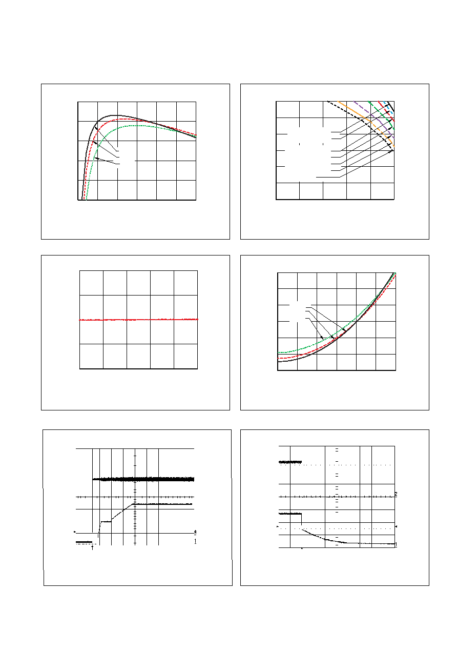
PKJ 4719E PI Typical Characteristics
Start-Up
Turn-Off
Start-up at Io=30A resistive load at T
Pcb
=+25 ∞C,
Vin=53 V. Start enabled by connecting Vin. Top trace:
input voltage (10 V/div.). Bottom trace: output voltage
(1 V/div.). Time scale: 5 ms/div.
Output voltage vs. load current at T
Pcb
=+25 ∞C, Vin=53 V.
Available load current vs. ambient air temperature and air-
fl ow at Vin=53 V. DC/DC converter mounted vertically with
airfl ow blowing from output pins toward input pins.
Effi ciency vs. load current and input voltage at T
Pcb
=+25 ∞C
0
5
10
15
20
25
30
70
75
80
85
90
95
[A]
[%]
36 V
53 V
75 V
0
20
40
60
80
100
0
5
10
15
20
25
30
[∞C]
[A]
2.0 m/s (400 lfm)
1.5 m/s (300 lfm)
1.0 m/s (200 lfm)
0.5 m/s (100 lfm)
Nat. Conv.
3.0 m/s (600 lfm)
2.5 m/s (500 lfm)
0
6
12
18
24
30
2.3
2.4
2.5
2.6
2.7
[A]
[V]
0
5
10
15
20
25
30
0
2
4
6
8
10
12
[A]
[W]
36 V
53 V
75 V
Dissipated power vs. load current and input voltage at
T
Pcb
=+25 ∞C
Turn-off at Io=30A resistive load at T
Pcb
=+25 ∞C,
Vin=53 V. Turn-off enabled by disconnecting Vin. Top
trace: output voltage (1 V/div.). Bottom trace: input
voltage (20 V/div.). Time scale: 10 ms/div.