e
1
5
10
15
20
25
30
1.0
1.5
2.0
2.5
3.0
3.5
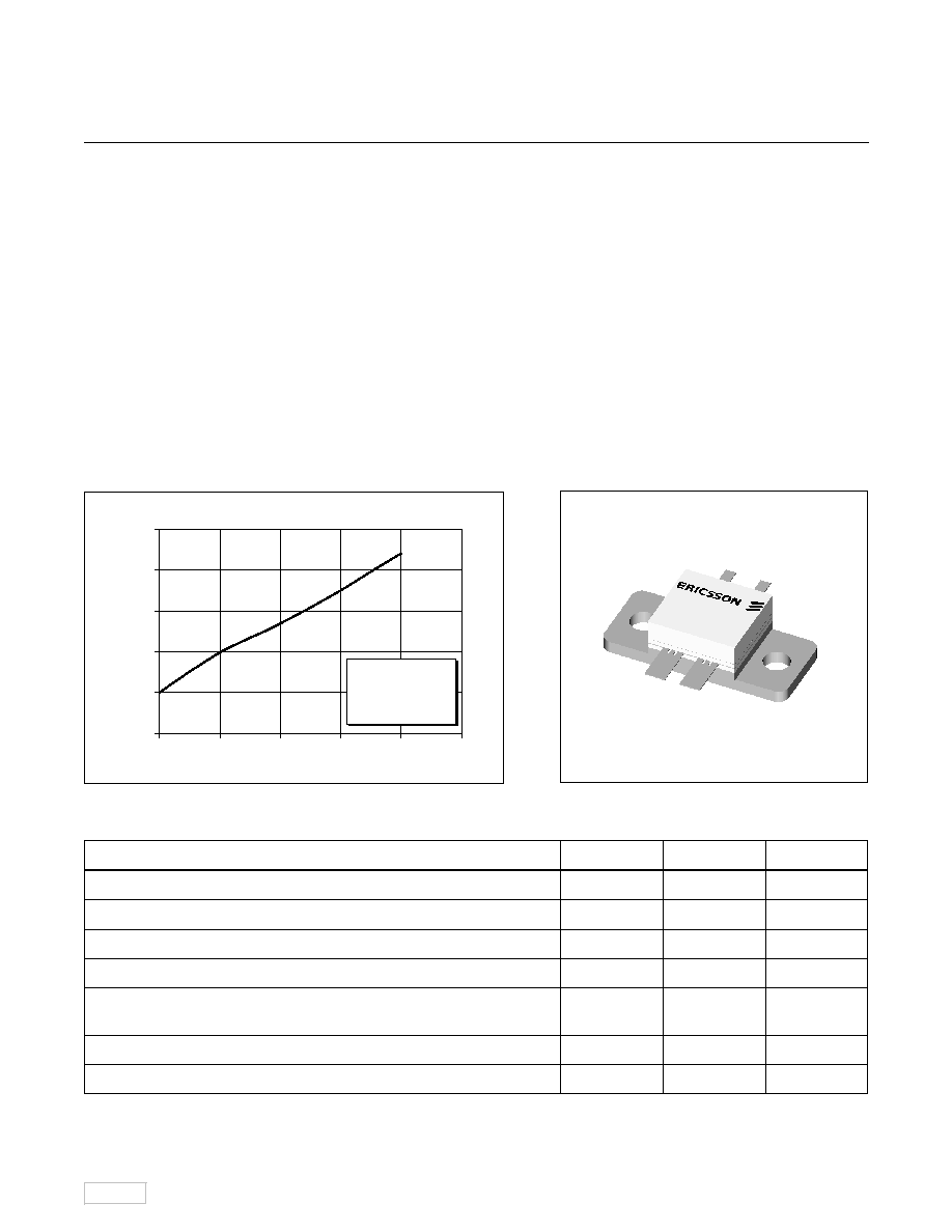
Input Power (Watts)
Output Power (Watts)
V
CC
= 26.5 V
I
CQ
= 3.0 A Total
f = 860 MHz
Typical Output Power vs. Input Power
Maximum Ratings
Parameter
Symbol
Value
Unit
Collector-Emitter Voltage
V
CER
40
Vdc
Collector-Base Voltage
V
CBO
65
Vdc
Emitter-Base Voltage (collector open)
V
EBO
4.0
Vdc
Collector Current (continuous)
I
C
9.0
Adc
Total Device Dissipation at Tflange = 25∞C
P
D
145
Watts
Above 25∞C derate by
0.83
W/∞C
Storage Temperature Range
T
STG
≠40 to +150
∞C
Thermal Resistance (Tflange = 70∞C)
R
JC
1.2
∞C/W
PTB 20011
20 Watts P-Sync, 470≠860 MHz
UHF TV Linear Power Transistor
Description
The 20011 is an NPN common emitter UHF power transistor intended
for 26.5 Vdc class A operation from 470 to 860 MHz. It is rated at 20
watts (p-sync) output power, and may be used for both CW and PEP
applications. Ion implantation, nitride surface passivation and gold
metallization ensure excellent device reliability. 100% lot traceability
is standard.
20 Watts (P-Sync), 470≠860 MHz
Class A Characteristics
Gold Metallization
Silicon Nitride Passivated
Package 20211
2001
1
LOT CODE
9/28/98
PTB 20011
2
e
Z Source
Z Load
Electrical Characteristics
(100% Tested)
Characteristic
Conditions
Symbol
Min
Typ
Max
Units
Breakdown Voltage C to E
I
B
= 0 A, I
C
= 50 mA
V(
BR)CEO
25
30
--
Volts
Breakdown Voltage C to E
V
BE
= 0 V, I
C
= 50 mA
V(
BR)CES
55
70
--
Volts
Breakdown Voltage E to B
I
C
= 0 A, I
E
= 5 mA
V(
BR)EBO
3.5
5
--
Volts
DC Current Gain
V
CE
= 5 V, I
C
= 250 mA
h
FE
20
50
100
--
Output Capacitance
V
CB
= 25 V, I
E
= 0 A, f = 1 MHz
C
ob
--
36
--
--
RF Specifications
(100% Tested)
Characteristic
Symbol
Min
Typ
Max
Units
Gain
(V
CC
= 26.5 Vdc, I
C
= 3.0 A Total, Pout = 20 W(P-sync),
G
pe
8.5
9.5
--
dB
f
1
= 860 MHz, Vision = -8dB, f
2
= 863.5 MHz, Subcarrier = -16dB,
f
3
= 864.5 MHz, Sound = -7dB)
Power Output (P-sync)
(V
CC
= 26.5 Vdc, I
C
= 3.0 A Total, f
1
= 860 MHz, Vision = -8dB,
Pout
20
--
--
Watts
f
2
= 863.5 MHz, Subcarrier = -16dB,
f
3
= 864.5 MHz, Sound = -7dB)
Intermodulation Distortion
(V
CC
= 26.5 Vdc, I
C
= 3.0 A Total, Pout = 20 W(P-sync),
IM
3
--
-48
-46
dBc
f
1
= 860 MHz, Vision = -8dB, f
2
= 863.5 MHz, Subcarrier = -16dB,
f
3
= 864.5 MHz, Sound = -7dB)
Load Mismatch Tolerance
(V
CC
= 26.5 Vdc, I
C
= 3.0 A Total, Pout = 20 W(P-sync),
--
--
3:1
--
f
1
= 860 MHz, Vision = -8dB, f
2
= 863.5 MHz, Subcarrier = -16dB,
f
3
= 864.5 MHz, Sound = -7dB--all phase angles at
frequency of test)
Impedance Data
(data shown for fixed-tuned broadband circuit)
(V
CC
= 26.5 Vdc, I
C
= 3.0 A Total, Pout = 20 W(P-sync)
Frequency
Z Source
Z Load
MHz
R
jX
R
jX
470
4.8
-25.0
9.0
15.0
665
10.0
-31.0
7.2
20.4
860
32.0
-36.0
6.4
25.4
5 /14/98
PTB 20011
3
e
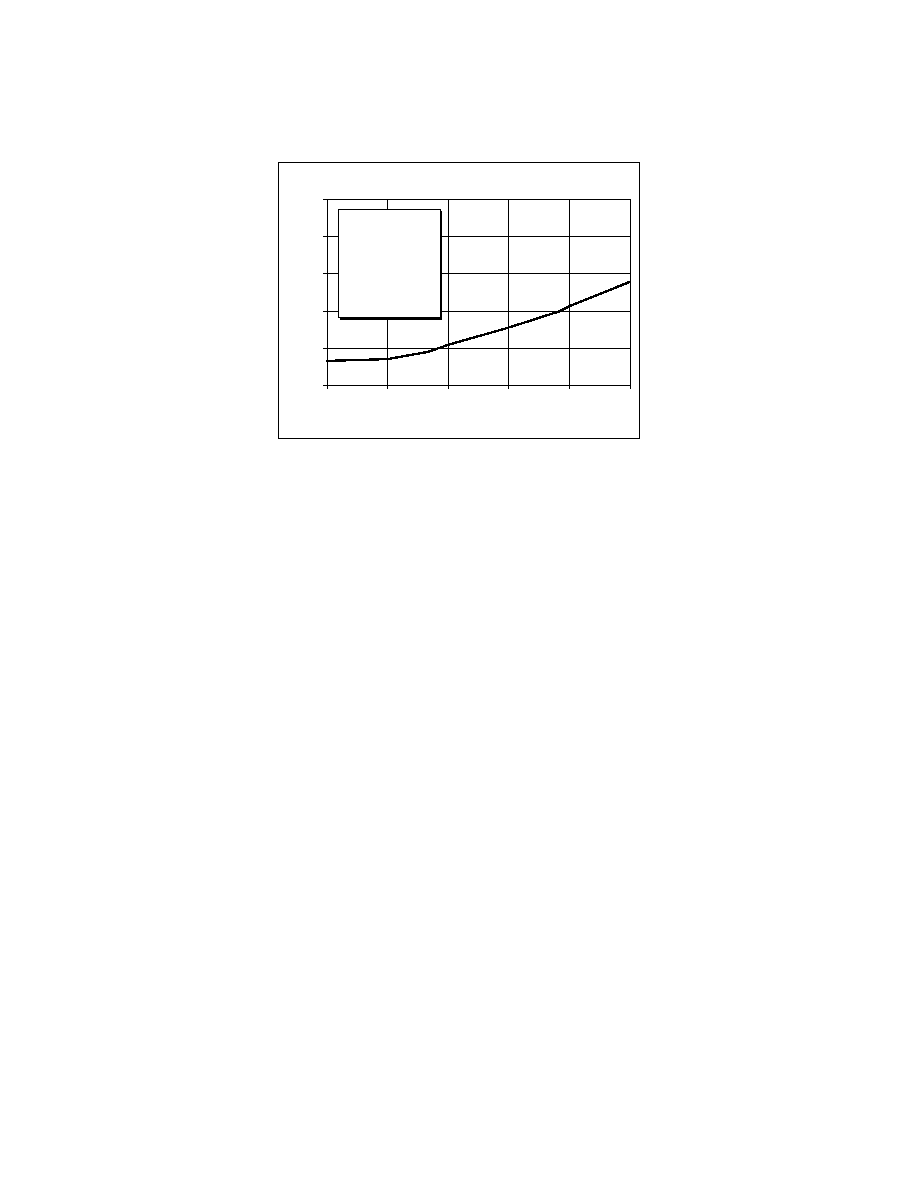
Intermodulation Distortion vs. Power Output
-70
-60
-50
-40
-30
-20
0
6
12
18
24
30
Output Power (Watts P-Sync)
IM
D (dBc
)
V
CC
= 26.5 V
I
C
= 3.0 A Total
f
1
= 860.0 MHz
f
2
= 863.5 MHz
f
3
= 864.5 MHz
Typical Performance
Ericsson Components
RF Power Products
675 Jarvis Drive
Morgan Hill, CA 95037 USA
Telephone: 408-778-9434
Specifications subject to change without notice.
LF
© Ericsson Components AB 1995
EUS/KR 1301-PTB 20011 Uen Rev. D 09-28-98
1-877-GOLDMOS
(1-877-465-3667)
e-mail: rfpower@ericsson.com
www.ericsson.com/rfpower