 | –≠–ª–µ–∫—Ç—Ä–æ–Ω–Ω—ã–π –∫–æ–º–ø–æ–Ω–µ–Ω—Ç: PTB20125 | –°–∫–∞—á–∞—Ç—å:  PDF PDF  ZIP ZIP |

e
1
Description
The 20125 is an NPN, push-pull RF power transistor intended for 26
Vdc class AB operation from 1.8 to 2.0 GHz. Rated at 100 watts PEP
minimum output power, it is specifically intended for operation as a
final stage in CDMA or TDMA systems. Ion implantation, nitride surface
passivation and gold metallization ensure excellent device reliability.
100% lot traceability is standard.
100 Watts, 1.8≠2.0 GHz
Class AB Characteristics
40% Collector Efficiency at 100 Watts
Gold Metallization
Silicon Nitride Passivated
PTB 20125
100 Watts, 1.8≠2.0 GHz
PCN/PCS Power Transistor
Package 20225 *
20125
LOT CODE
5
6
7
8
9
10
11
12
1750
1800
1850
1900
1950
2000
2050
Frequency (MHz)
G
a
in (dB)
20
40
60
80
100
120
140
Output Power & Efficiency
V
CC
= 26 V
I
CQ
= 200 mA
Typical P
OUT
, Gain & Efficiency
(at P-1dB)
vs. Frequency
Output Power (W)
Efficiency (%)
Gain (dB)
Maximum Ratings
Parameter
Symbol
Value
Unit
Collector-Emitter Voltage
V
CER
55
Vdc
Collector-Base Voltage
V
CBO
55
Vdc
Emitter-Base Voltage (collector open)
V
EBO
4.0
Vdc
Collector Current (continuous)
I
C
14
Adc
Total Device Dissipation at Tflange = 25∞C
P
D
400
Watts
Above 25∞C derate by
2.3
W/∞C
Storage Temperature Range
T
STG
≠40 to +150
∞C
Thermal Resistance (Tflange = 70∞C)
R
JC
0.44
∞C/W
* This product not recommended or specified for CW or class A operation. Recommend two PTB 20175 for these applications.
5 /1 9 /9 8

PTB 20125
2
e
Electrical Characteristics
(100% Tested)
Characteristic
Conditions
Symbol
Min
Typ
Max
Units
Breakdown Voltage C to E
V
BE
= 0 V, I
C
= 100 mA
V
(BR)CES
55
--
--
Volts
Breakdown Voltage E to B
I
C
= 0 A, I
E
= 20 mA
V
(BR)EBO
4.0
5.0
--
Volts
DC Current Gain
V
CE
= 10 V, I
C
= 1.5 A
h
FE
30
50
120
--
RF Specifications
(100% Tested)
Characteristic
Symbol
Min
Typ
Max
Units
Gain
(V
CC
= 26 Vdc, Pout = 40 W(PEP), I
CQ
= 2 x 100 mA, f = 2 GHz)
G
pe
7.0
8.0
--
dB
Collector Efficiency
(V
CC
= 26 Vdc, Pout = 100 W, I
CQ
= 2 x 100 mA, f = 2 GHz)
C
40
45
--
%
Load Mismatch Tolerance
(V
CC
= 26 Vdc, Pout = 100 W(PEP), I
CQ
= 2 x 100 mA, f = 2 GHz
--
--
5:1
--
--at all phase angles)
Typical Performance
Broadband Test Fixture Performance
0
2
4
6
8
10
1900
1925
1950
1975
2000
Frequency (MHz)
G
a
in (dB)
0
10
20
30
40
50
60
V
CC
= 26 V
I
CQ
= 200 mA
Pout = 50 W
Gain (dB)
Return Loss (dB)
Efficiency (%)
Efficiency (%
)
Re
turn Los
s
(dB
)
- 5
-15
-25
-35
Output Power vs. Supply Voltage
70
80
90
100
110
120
130
140
22
23
24
25
26
27
Supply Voltage (Volts)
Output Power (Watts)
I
CQ
= 200 mA
f = 2000 MHz
PTB 20125
3
e
Power Gain vs. Output Power
5
6
7
8
9
10
0.1
1.0
10.0
100.0
Output Power (Watts)
Po
we
r Ga
i
n
(d
B)
V
CC
= 26 V
f = 2000 MHz
I
CQ
= 200 mA
I
CQ
= 100 mA
I
CQ
= 50 mA
0
20
40
60
80
100
120
140
160
0
5
10
15
20
25
30
Input Power (Watts)
Output Power (Watts)
Vcc = 26 V
I
CQ
= 200 mA
f = 2000 MHz
Typical Output Power vs. Input Power
Intermodulation Distortion vs. Power Output
-40
-39
-38
-37
-36
-35
-34
-33
-32
-31
-30
10
20
30
40
50
60
70
80
90
100
Output Power (Watts-PEP)
IM
D (dBc
)
V
CC
= 26 V
I
CQ
= 2 x 50 mA
f
1
= 1.999 GHz
f
2
= 1.998 GHz
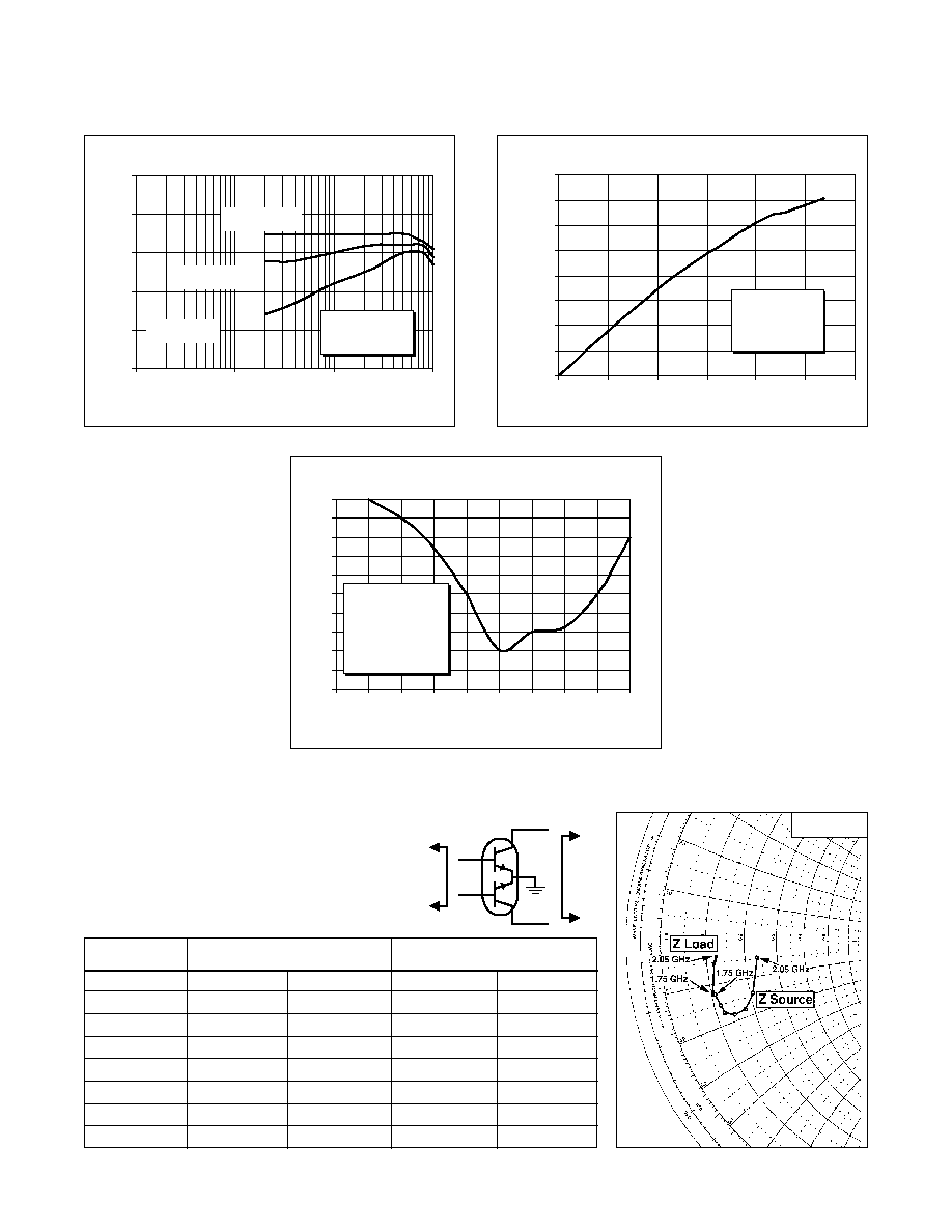
Z Source
Z Load
Frequency
Z Source
Z Load
GHz
R
jX
R
jX
1.75
5.4
-6.2
5.1
-6.2
1.80
5.8
-7.6
5.2
-5.8
1.85
6.0
-8.6
5.4
-5.0
1.90
7.2
-9.2
5.6
-4.0
1.95
8.8
-9.0
5.8
-2.8
2.00
10.4
-7.2
6.0
-2.4
2.05
11.8
-2.4
6.2
-1.8
Impedance Data
(V
CC
= 26 Vdc, Pout = 100 W, I
CQ
= 2 x 100 mA)
Z
0
= 50

PTB 20125
4
e
Placement Diagram (not to scale)
Test Circuit
Block Diagram for f = 2 GHz
Q1
PTB 20125 NPN RF Transistor
l
1,
l
2,
l
21,
l
22
.25
2GHz Microstrip 50
l
3,
l
4
.085
2GHz Microstrip 80
l
5,
l
6
.067
2GHz Microstrip 20
l
7,
l
8,
l
11,
l
12
.0217
2GHz Microstrip 11.7
l
9,
l
10
.053
2GHz Microstrip 8.15
l
13,
l
14
.055
2GHz Microstrip 6.7
l
15,
l
16
.052
2GHz Microstrip 11.45
l
17,
l
18
.060
2GHz Microstrip 16.9
l
19,
l
20
.252
2GHz Microstrip 75
Q1
L1, L2
6.8 nh SMT Inductor
L3, L4
56 nh SMT Inductor
L5, L6
4 mm. SMT Ferrite
C1, C2
0≠4 pF Johanson Piston Trimmer
C3-8, C17, C18
33 pF (B ATC 100)
C9, C11, C13, C15
.1
µ
F 1206
C10, C12, C14, C16
10
µ
F SMT Tantalum
R1, R2
22
SMT
T1, T2
UT 70-50
Board
0.031: G200, Solid Copper
Bottom, AlliedSignal

PTB 20125
5
e
Artwork (1 inch
)
Ericsson Components
RF Power Products
675 Jarvis Drive
Morgan Hill, CA 95037 USA
Telephone: 408-778-9434
Specifications subject to change without notice.
L3
© 1996 Ericsson Inc.
EUS/KR 1301-PTB 20125 Uen Rev. C 09-28-98
1-877-GOLDMOS
(1-877-465-3667)
e-mail: rfpower@ericsson.com
www.ericsson.com/rfpower