
e
1
Description
The 20175 is a class AB, NPN common emitter RF power transistor
intended for 26 Vdc operation from 1.9 to 2.0 GHz. It is rated at 55
watts minimum output power and may be used for both CW and PEP
applications. Ion implantation, nitride surface passivation and gold
metallization are used to ensure excellent device reliability. 100% lot
traceability is standard.
PTB 20175
55 Watts, 1.9≠2.0 GHz
Cellular Radio RF Power Transistor
20175
LOT CODE
10
20
30
40
50
60
70
2
4
6
8
10
12
14
Input Power (Watts)
Output Power (Watts)
V
CC
= 26 V
I
CQ
= 0.150 A
f = 2 GHz
Typical Output Power vs. Input Power
Package 20223
Maximum Ratings
Parameter
Symbol
Value
Unit
Collector-Emitter Voltage
V
CER
55
Vdc
Collector-Emitter Voltage
V
CES
55
Vdc
Emitter-Base Voltage (collector open)
V
EBO
4
Vdc
Collector Current (continuous)
I
C
8
Adc
Total Device Dissipation at Tflange = 25∞ C
P
D
233
W
Above 25∞C derate by
1.33
W/∞C
Storage Temperature Range
Tstg
≠40 to +150
∞C
Thermal Resistance (Tflange = 70∞ C)
R
JC
.75
∞C/W
55 Watts, 1.9≠2.0 GHz
Class AB Characteristics
40% Collector Efficiency at 55 Watts
Gold Metallization
Silicon Nitride Passivated
9/28/98

PTB 20175
2
e
Z Source
Z Load
Electrical Characteristics
(100% Tested)
Characteristics
Conditions
Symbol
Min
Typ
Max
Units
Breakdown Voltage C to E
Ic = 60 mA, R
B
= 27
V
(BR)CER
55
--
--
Volts
Breakdown Voltage C to E
V
BE
= 0 V, I
C
= 60 mA
V
(BR)CES
55
--
--
Volts
Breakdown Voltage E to B
I
C
= 0 V, I
E
= 25 mA
V
(BR)EBO
4.0
5
--
Volts
DC Current Gain
V
CE
= 5 V, I
C
= 300 mA
H
fe
--
50
--
--
RF Specifications
(100% Tested)
Characteristics
Symbol
Min
Typ
Max
Units
Gain
(V
CC
= 26 Vdc, Pout = 55 W, I
CQ
= 150 mA,
G
pe
7.0
7.6
--
dB
f = 2.0 GHz)
Collector Efficiency
(V
CC
= 26 Vdc, Pout = 55 W, I
CQ
= 150 mA,
C
37
47
--
%
f = 2.0 GHz)
Load Mismatch Tolerance
(V
CC
= 26 Vdc, Pout = 55 W(PEP), I
CQ
= 150 mA,
--
--
5:1
--
f = 2.0 GHz--All Phase Angles at Frequency of Test)
Impedance Data
(data shown for fixed-tuned broadband circuit)
(V
CC
= 26 Vdc, Pout = 55 W, I
CQ
= 150 mA)
Frequency
Z Source
Z Load
GHz
R
jX
R
jX
1.90
3.26
-2.0
2.30
-1.9
1.95
3.26
-1.7
2.25
-2.2
2.00
3.26
-1.4
2.20
-2.5
Z
0
= 50
5 /19/98
PTB 20175
3
e
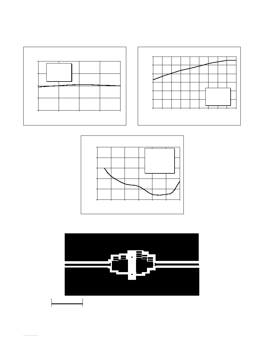
Typical Performance
Test Circuit
Gain vs. Frequency
(as measured in a broadband circuit)
7.0
7.5
8.0
8.5
9.0
1.90
1.93
1.95
1.98
2.00
Frequency (GHz)
Ga
in
(d
B)
V
CC
= 26 V
I
CQ
= 0.150 A
Pout = 15 W
Efficiency vs. Output Power
0
10
20
30
40
50
60
20
25
30
35
40
45
50
55
60
65
Output Power (Watts)
Efficiency (%)
V
CC
= 26 V
I
CQ
= 0.150 A
f = 2 GHz
Intermodulation Distortion vs. Power Output
-40
-36
-32
-28
-24
-20
0
10
20
30
40
50
60
Output Power (Watts-PEP)
IM
D (dBc
)
V
CC
= 26 V
I
CQ
= 0.150 A
f
1
= 1.999 GHz
F
2
= 2.000 GHz
Artwork (1 inch
)
5/19/98
PTB 20175
4
e
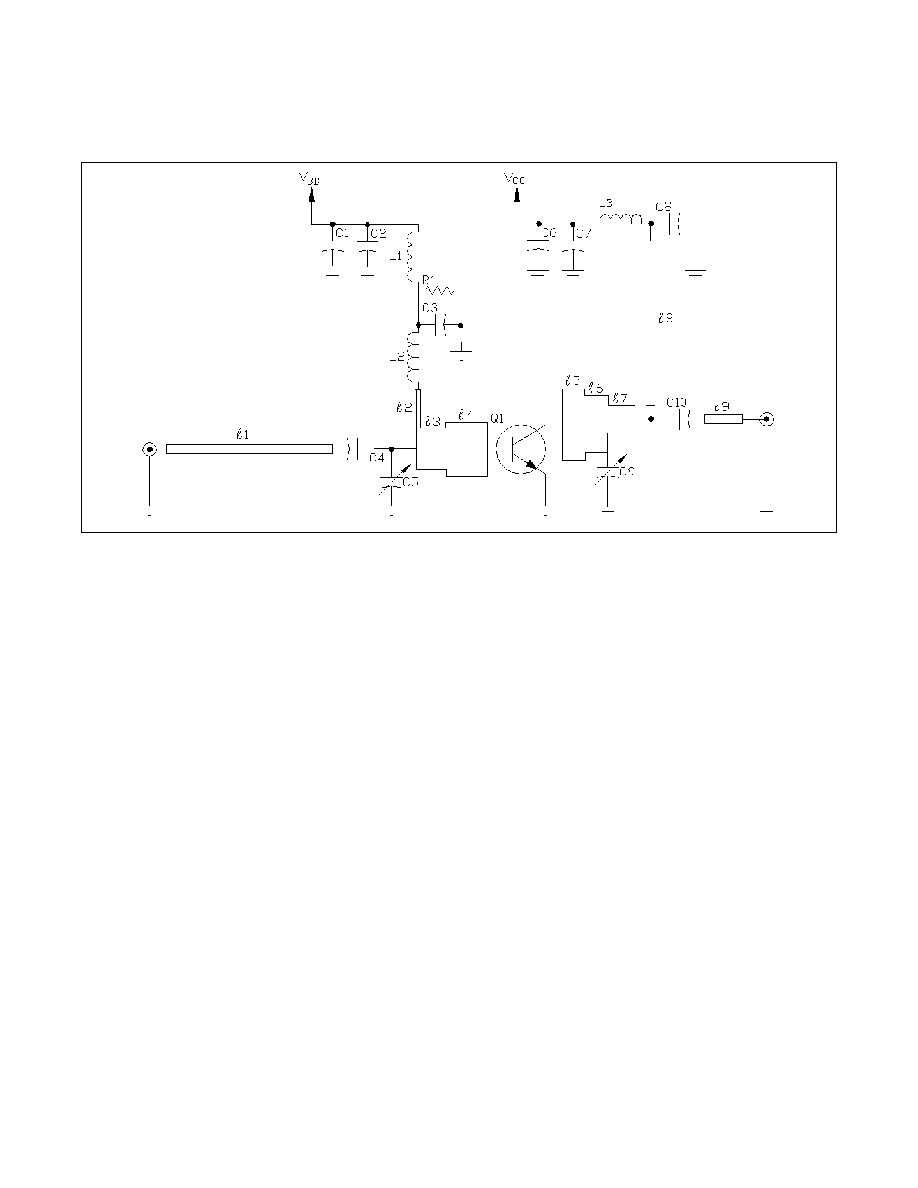
Schematic for f = 2 GHz
Q1
PTB 20175
NPN RF Transistor
l
1
Microstrip 50
l
2
.1
2 GHz
Microstrip 75
l
3
.065
2 GHz
Microstrip 16
l
4
.095
2 GHz
Microstrip 10.8
l
5
.055
2 GHz
Microstrip 8.0
l
6
.055
2 GHz
Microstrip 12.5
l
7
.065
2 GHz
Microstrip 22
l
8
.25
2 GHz
Microstrip 60
l
9
Microstrip 50
C1, C6
.1
µ
F
1206 Chip
C2, C7
10
µ
F, 35 V
SMT Tantalum
C3, C4, C8, C10
33 pF
ATC-100
C5, C9
0 - 4 pf
Johanson Trimmer
L1
56 nh
SMT Inductor
L2
6.8 nh
SMT Inductor
L3
4 mm.
SMT Ferrite
R1
22
1206 Chip
Board
.031 G-200 Solid Copper Bottom
Ericsson Components
RF Power Products
675 Jarvis Drive
Morgan Hill, CA 95037 USA
Telephone: 408-778-9434
Specifications subject to change without notice.
LF
© 1996 Ericsson Inc.
EUS/KR 1301-PTB 20175 Uen Rev. C 09-28-98
1-877-GOLDMOS
(1-877-465-3667)
e-mail: rfpower@ericsson.com
www.ericsson.com/rfpower