 | –≠–ª–µ–∫—Ç—Ä–æ–Ω–Ω—ã–π –∫–æ–º–ø–æ–Ω–µ–Ω—Ç: PTF10112 | –°–∫–∞—á–∞—Ç—å:  PDF PDF  ZIP ZIP |

e
1
PTF 10112
60 Watts, 1.8≠2.0 GHz
GOLDMOS
TM
Field Effect Transistor
Package 20248
0
20
40
60
80
0
1
2
3
4
5
6
Input Power (Watts)
Output Power (Watts)
V
CC
= 28 V
I
DQ
= 580 mA
f = 2000 MHz
Typical Output Power vs. Input Power
Description
The PTF 10112 is an internally matched common source N-channel
enhancement-mode lateral MOSFET intended for CDMA and TDMA
applications from 1.8 to 2.0 GHz. It is rated at 60 watts power output.
Nitride surface passivation and full gold metallization ensure excellent
device lifetime and reliability.
∑
INTERNALLY MATCHED
∑
Guaranteed Performance at 1.93, 1.99 GHz,
28 V
- Output Power = 60 Watts Min
- Power Gain = 12 dB Typ
∑
Full Gold Metallization
∑
Silicon Nitride Passivated
∑
Back Side Common Source
∑
Excellent Thermal Stability
∑
100% Lot Traceability
RF Specifications
(100% Tested)
Characteristic
Symbol
Min
Typ
Max
Units
Gain
(V
DD
= 28 V, P
OUT
= 15 W, I
DQ
= 580 mA, f = 1.93, 1.99 GHz)
G
ps
11
12
--
dB
Power Output at 1 dB Compression
(V
DD
= 28 V, I
DQ
= 580 mA, f = 1.99 GHz)
P-1dB
60
--
--
Watts
Drain Efficiency
(V
DD
= 28 V, P
OUT
= 60 W, I
DQ
= 580 mA, f = 1.99 GHz)
h
D
--
41
--
%
Load Mismatch Tolerance
(V
DD
= 28 V, P
OUT
= 60 W, I
DQ
= 580 mA, f = 1.99 GHz
Y
--
--
10:1
--
--all phase angles at frequency of test)
All published data at T
CASE
= 25∞C unless otherwise indicated.
10112
A-1234569837
PTF 10112
2
e
Electrical Characteristics
(100% Tested)
Characteristic
Conditions
Symbol
Min
Typ
Max
Units
Drain-Source Breakdown Voltage
V
GS
= 0 V, I
D
= 100 mA
V
(BR)DSS
65
--
--
Volts
Zero Gate Voltage Drain Current
V
DS
= 28 V, V
GS
= 0 V
I
DSS
--
--
5.0
mA
Gate Threshold Voltage
V
DS
= 10 V, I
D
= 150 mA
V
GS(th)
3.0
--
5.0
Volts
Forward Transconductance
V
DS
= 10 V, I
D
= 2 A
g
fs
--
4.0
--
Siemens
Maximum Ratings
Parameter
Symbol
Value
Unit
Drain-Source Voltage
V
DSS
65
Vdc
Gate-Source Voltage
V
GS
±20
Vdc
Operating Junction Temperature
T
J
200
∞C
Total Device Dissipation at
P
D
237
Watts
Above 25∞C derate by
1.35
W/∞C
Storage Temperature Range
T
STG
≠40 to +150
∞C
Thermal Resistance (T
CASE
= 70∞C)
R
q
JC
0.74
∞C/W
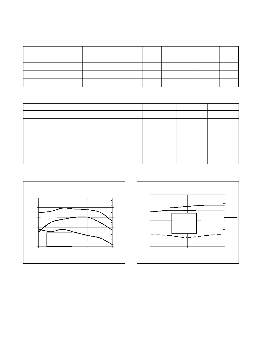
Typical Performance
9
10
11
12
13
14
1750
1850
1950
2050
Frequency (MHz)
G
a
in (dB)
30
40
50
60
70
80
Output Power & Efficienc
y
V
CC
= 28 V
I
DQ
= 580 mA
Output Power (W)
Efficiency (%)
Gain (dB)
Typical P
OUT
, Gain & Efficiency
(at P-1dB)
vs. Frequency
Broadband Test Fixture Performance
9
10
11
12
13
1930
1940
1950
1960
1970
1980
1990
Frequency (MHz)
G
a
in (dB)
0
10
20
30
40
50
60
V
DD
= 28 V
I
DQ
= 580mA
P
OUT
= 20 W
Gain (dB)
Return Loss (dB)
Efficiency (%)
@P-1dB
Efficiency (%
)
Return Loss (dB
)
0
-10
-20
-30

PTF 10112
3
e
Output Power vs. Supply Voltage
40
50
60
70
80
22
24
26
28
30
32
34
Supply Voltage (Volts)
Output Power (Watts)
I
DQ
= 580 mA
f = 2000 MHz
-65
-55
-45
-35
-25
-15
0
10
20
30
40
50
60
70
Output Power (Watts-PEP)
IM
D (dBc
)
V
DD
= 28 V
I
DQ
= 580 mA
f
1
= 1959 MHz
f
2
= 1960 MHz
Intermodulation Distortion vs. Output Power
(as measured in a broadband circuit)
IM3
IM7
IM5
Power Gain vs. Output Power
7
8
9
10
11
12
13
14
0.1
1.0
10.0
100.0
Output Power (Watts)
Po
we
r Ga
i
n
(d
B)
V
DD
= 28 V
f = 2000 MHz
I
DQ
= 580 mA
I
DQ
= 290 mA
I
DQ
= 145 mA
Capacitance vs. Supply Voltage *
0
40
80
120
160
200
240
0
10
20
30
40
Supply Voltage (Volts)
Cds and Cgs (pF)
0
6
12
18
24
Crs
s
C
gs
C
ds
C
rss
V
GS
= 0 V
f = 1 MHz
* This part is internally matched. Measurements of the finished
product will not yield these results.
Bias Voltage vs. Temperature
0.95
0.96
0.97
0.98
0.99
1.00
1.01
1.02
1.03
-20
30
80
130
Temp. (∞C)
B
i
as V
o
ltage (V
)
0.400
1.383
2.367
3.350
4.333
5.317
Voltage normalized to 1.0 V
Series show current (A)
PTF 10112
4
e
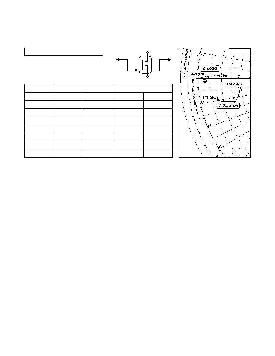
Frequency
Z Source
W
Z Load
W
GHz
R
jX
R
jX
1.75
3.74
-4.50
1.48
0.25
1.80
3.80
-4.80
1.56
-0.20
1.85
3.96
-5.10
1.66
-0.50
1.90
4.90
-5.50
1.32
-0.80
1.95
7.90
-6.10
1.16
-0.60
2.00
9.00
-4.60
1.10
-0.45
2.05
10.00
-1.70
1.18
-0.30
Impedance Data
V
DD
= 28 V, P
OUT
= 60 W, I
DQ
= 580 mA
Z Source
Z Load
G
S
D
Z
0
= 50
W
PTF 10112
5
e
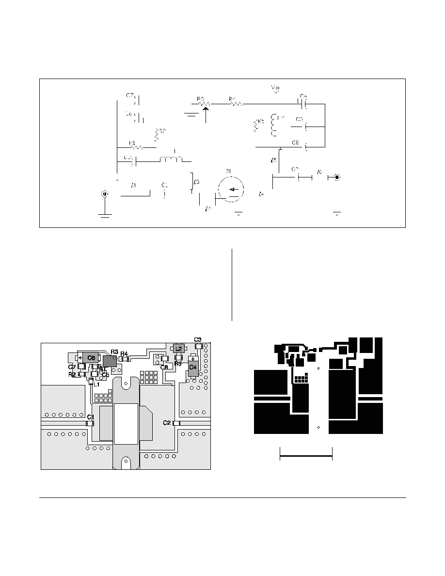
Test Circuit
Test Circuit Block Diagram for f = 1.93≠1.99 GHz
Q1
PTF 10112
LDMOS RF Transistor
l
1,
l
6
Microstrip 50
W
l
2
.10
l
@ 2.0 GHz
Microstrip 9.4
W
l
3
.08
l
@ 2.0 GHz
Microstrip 70
W
l
4
.162
l
@ 2.0 GHz
Microstrip 5.8
W
l
5
.22
l
@ 2 GHz
Microstrip 65
W
C1, C2, C5, C8
10 pF Chip Cap
ATC 100 B
C3, C7
0.1
m
F Chip Cap
C4, C6
10
m
F SMT Tantalum
Parts Layout (not to scale)
Artwork (1 inch
)
L1
2.7 nh
SMT Coil
L2
4mm
SMT Ferrite Bead
R1, R2
220
W
Chip Resistor K1206
R3
2K
SMT Potentiometer
R4
10
W
Chip Resistor K1206
R5
1
W
Chip Resistor K1206
Circuit Board
.028" Dielectric Thickness,
e
r
= 4.0,
AlliedSignal, G200, 2 oz. copper
e
10112
Ericsson Microelectronics
RF Power Products
Morgan Hill, CA 95037 USA
Specifications subject to change without notice.
L3
© 1998 Ericsson Inc.
EUS/KR 1301-PTF 10112 Uen Rev. A 01-08-2000
1-877-GOLDMOS (465-3667) United States
+46 8 757 4700 International
e-mail: rfpower@ericsson.com
www.ericsson.com/rfpower

6
e
Notes: