
ESMT
M32L1632512A
Elite Semiconductor Memory Technology Inc.
Publication Date : Jun. 2001
Revision : 1.6
1/54
SGRAM
256K
x 32 Bit x 2 Banks
Synchronous Graphic RAM
FEATURES
JEDEC standard 3.3V power supply
LVTTL compatible with multiplexed address
Dual bank / Pulse RAS
MRS cycle with address key programs
- CAS Latency ( 2, 3 )
- Burst Length ( 1, 2, 4, 8 & full page )
- Burst Type ( Sequential & Interleave )
All inputs are sampled at the positive going
edge of the system clock
Burst Read Single-bit Write operation
DQM 0-3 for byte masking
Auto & self refresh
32ms refresh period (2K cycle)
100 pin QFP
Graphic Features
SMRS cycle
- Load mask register
- Load color register
Write Per Bit
Block Write (8 Columns)
GENERAL DESCRIPTION
The M32L1632512A is 16, 777, 216 bits synchro-
nous high data rate Dynamic RAM organized as 2 x
262, 144 words by 32 bits, fabricated with ESMT's
high performance CMOS technology. Synchronous
design allows precise cycle control with the use of
system clock. I/O transactions are possible on every
clock cycle. Range of operating frequencies , progra-
mmable burst length, and programmable latencies
allows the same device to be useful for a variety of
high bandwidth, high performance memory system
applications.
Write per bit and 8 columns block write improves
performance in graphic systems.
ORDERING INFORMATION
Part NO.
Cycle
time
Clock
Frequency
Access
time@CL=3
t
RDL
(clk)
M32L1632512A-5Q
5ns
200MHz
4.5ns
1
M32L1632512A-5SQ
5ns
200MHz
4.5ns
2
M32L1632512A-6Q
6ns
166MHz
5.5ns
1
M32L1632512A-6SQ
6ns
166MHz
5.5ns
2
M32L1632512A-7Q
7ns
143MHz
6.0ns
1
M32L1632512A-7SQ
7ns
143MHz
6.0ns
2
M32L1632512A-8Q
8ns
125MHz
6.5ns
1
M32L1632512A-8SQ
8ns
125MHz
6.5ns
2

ESMT
M32L1632512A
Elite Semiconductor Memory Technology Inc.
Publication Date : Jun. 2001
Revision : 1.6
2/54
FUNCTIONAL BLOCK DIAGRAM
PIN CONFIGURATION (TOP VIEW)
BLOCK
WRITE
CONTROL
LOGIC
DQMi
WRITE
CONTROL
LOGIC
MA
S
K
MUX
MASK
REGISTER
COLOR
REGISTER
COLUMN
MASK
I
N
PU
T
B
U
FFE
R
PR
OG
R
A
M
I
N
G
R
E
G
I
S
T
E
R
COLU
MN
DE
C
O
RDE
R
SE
N
S
E
A
M
P
L
IF
IE
R
256Kx32
CELL
ARRAY
256Kx32
CELL
ARRAY
OU
T
P
U
T
B
U
FFE
R
ROW DECORDER
BANK SELECTION
SERIAL
COUNTER
COLUMN ADDRESS
BUFFER
ROW ADDRESS
BUFFER
REFRESH
COUNTER
ADDRESS REGISTER
CLOCK
ADDRESS(A
0
~A
10
)
DQMi
DQi
(i=0~31)
T
I
M
I
NG R
E
G
I
S
T
E
R
CLK
CKE
CS
RAS
CAS
WE
DSF
DQMi
LA
TE
N
C
Y
&
BU
RS
T
L
E
N
G
T
H
DQ
2
8
VD
D
Q
DQ
2
7
DQ
2
6
V
SSQ
DQ
2
5
DQ
2
4
DQ
1
5
DQ
1
4
V
DDQ
DQ
1
3
DQ
1
2
V
SSQ
DQ
1
1
V
SS
DQ
1
0
V
DD
DQ
9
DQ
8
V
SSQ
DQ
M
3
V
DDQ
N.
C
CL
K
CK
E
DQ
M
1
N.
C
A
9
DS
F
80
79
78
77
75
74
76
72
71
73
69
70
68
65
67
64
66
62
61
63
59
58
60
56
55
57
53
54
52
V
DDQ
51
DQ
3
DQ
4
DQ
5
DQ
6
DQ
7
V
SSQ
DQ
1
6
DQ
1
7
V
DDQ
DQ
1
8
V
SSQ
DQ
1
9
DQ
2
0
V
SS
DQ
2
1
V
DD
DQ
2
2
DQ
2
3
V
SS
Q
DQ
M
0
DQ
M
2
V
DDQ
V
DDQ
WE
BA(
A
10
)
A
8
1
2
3
4
6
7
5
9
10
8
12
11
13
14
16
17
15
19
20
18
22
23
21
25
26
24
28
27
29
30
V
DDQ
CA
S
RA
S
CS
50
49
48
47
45
44
46
42
41
43
39
40
38
37
35
34
36
32
31
33
81
82
83
84
86
87
85
89
90
88
92
91
93
94
96
97
95
99
100
98
DQ29
DQ 0
V
DD
DQ 1
V
SSQ
DQ 2
V
SSQ
DQ30
DQ31
V
SS
N. C
N. C
N. C
N. C
N. C
N. C
1&
1&
1&
1&
3 L Q
4 ) 3
) R U Z D U G
7 \ S H
[
P P
P P S L Q
3 L W F K
$
$
$
$
966
1&
1&
1&
1&
1&
1&
1&
1&
1&
1&
$
$
$
$
9''
ESMT
M32L1632512A
Elite Semiconductor Memory Technology Inc.
Publication Date : Jun. 2001
Revision : 1.6
3/54
PIN DESCRIPTION
PIN
NAME
INPUT FUNCTION
CLK
System Clock
Active on the positive going edge to sample all inputs
CS
Chip Select
Disables or enable device operation by masking or enabling all
inputs except CLK, CKE and DQMi
CKE
Clock Enable
Masks system clock to freeze operation from the next clock cycle.
CKE should be enabled at least one clock+
t
ss prior to new
command.
Disable input buffers for power down in standby.
A0 ~ A9
Address
Row / column addresses are multiplexed on the same pins.
Row address : RA0~RA9, column address : CA0~CA7
A10(BA)
Bank Select Address
Selects bank to be activated during row address latch time.
Selects bank for read / write during column address latch time.
RAS
Row Address Strobe
Latches row addresses on the positive going edge of the CLK with
RAS low.
Enables row access & precharge.
CAS
Column Address Strobe
Latches column address on the positive going edge of the CLK
With
CAS low.
Enables column access.
WE
Write Enable
Enables write operation and Row precharge.
DQMi
Data Input/Output Mask
Makes data output Hi-Z,
t
SHZ
after the clock and masks the output.
Blocks data input when DQM active. (Byte Masking)
DQi
Data Input/Output
Data inputs/outputs are multiplexed on the same pins.
DSF
Define Special/ Function
Enables write per bit, block write and special mode register set.
V
DD
/V
SS
Power Supply/ Ground
V
DDQ
/V
SSQ
Data Output Power/Ground
ABSOLUTE MAXIMUM RATINGS
(Voltage referenced to V
SS
)
Parameter
Symbol
Value
Unit
Voltage on any pin relative to V
SS
V
IN
, V
OUT
-1.0 ~ 4.6
V
Voltage on V
DD
supply relative to V
SS
V
DD
, V
DDQ
-1.0 ~ 4.6
V
Storage temperature
T
STG
-55 ~ +150
i
Power dissipation
P
D
1
W
Short circuit current
I
OS
50
mA
Note : Permanent device damage may occur if "ABSOLUTE MAXIMUM RATINGS" are exceeded.
Functional operation should be restricted to recommended operating condition.
Exposure to higher than recommended voltage for extended periods of time could affect device
reliability.
ESMT
M32L1632512A
Elite Semiconductor Memory Technology Inc.
Publication Date : Jun. 2001
Revision : 1.6
4/54
DC OPERATING CONDITIONS
Recommended operating conditions (Voltage referenced to V
SS
= 0V)
Parameter
Symbol
Min
Typ
Max
Unit
Note
Supply voltage
V
DD
, V
DDQ
3.0
3.3
3.6
V
Input high voltage
V
IH
2.0
3.0
V
DD
+0.3
V
Input low voltage
V
IL
-0.3
0
0.8
V
Note 1
Output high voltage
V
OH
2.4
-
-
V
I
OH
= -2mA
Output low voltage
V
OL
-
-
0.4
V
I
OL
= 2mA
Input leakage current
I
IL
-5
-
5
�A
Note 2
Output leakage current
I
OL
-5
-
5
�A
Note 3
Output Loading Condition
See Fig 1
Note: 1. V
IL
(min) = -1.5V AC (pulse width
5ns)
2. Any input 0V
V
IN
V
DD
+ 0.3V, all other pins are not under test = 0V.
4. Dout is disabled, 0V
V
OUT
V
DD
.
CAPACITANCE
(V
DD
/V
DDQ
= 3.3V, T
A
= 25 C
� , f = 1MH
Z
)
Parameter
Symbol
Min
Max
Unit
Input capacitance (A0 ~ A10)
C
IN1
-
4
pF
Input capacitance
(CLK, CKE, CS , RAS , CAS , WE , DSF& DQM0-3)
C
IN2
-
4
pF
Data input/output capacitance (DQ0 ~ DQ31)
C
OUT
-
5
pF
DECOUPLING CAPACITANCE GUIDE LINE
Recommended decoupling capacitance added to power line at board.
Parameter
Symbol
Value
Unit
Decoupling Capacitance between V
DD
& V
SS
C
DC1
0.1+0.01
uF
Decoupling Capacitance between V
DDQ
& V
SSQ
C
DC2
0.1+0.01
uF
*Note: 1. V
DD
and V
DDQ
pins are separated each other.
All V
DD
pins are connected in chip. All V
DDQ
pins are connected in chip.
2. V
SS
and V
SSQ
pins are separated each other.
All V
SS
pins are connected in chip. All V
SSQ
pins are connected in chip.
ESMT
M32L1632512A
Elite Semiconductor Memory Technology Inc.
Publication Date : Jun. 2001
Revision : 1.6
5/54
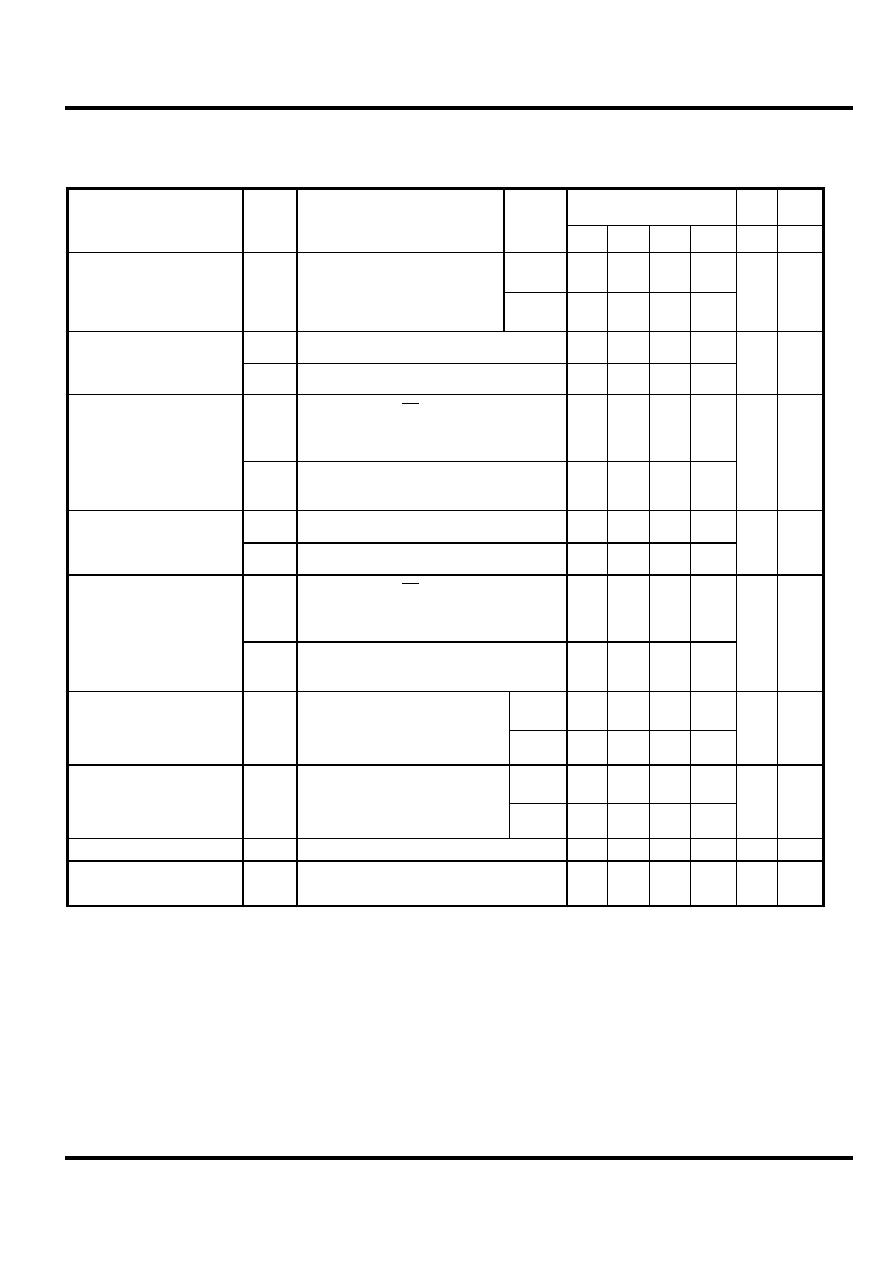
DC CHARACTERISTICS
Recommended operating condition unless otherwise noted, T
A
= 0 to 70 C
� V
IH(min)
/V
IL(max)
=2.0V/0.8V
Version
Unit Note
Parameter
Symbol
Test Condition
CAS
Latency -5/5S -6/6S -7/7S -8/8S
3
230
210
195
170
Operating Current
(One Bank Active)
I
CC1
Burst Length = 1
t
RC
t
RC(min)
,
t
CC
t
CC(min)
I
OL
= 0 mA
2
230
210
195
170
mA
1
I
CC2
P CKE
V
IL(max)
,
t
CC
= 15ns
2
2
2
2
Precharge Standby Current
in power-down mode
I
CC2
PS CKE
V
IL(max)
, CLK
V
IL(max)
,
t
CC
=
2
2
2
2
mA
I
CC2
N CKE
V
IH(min)
, CS
V
IH(min)
,
t
CC
= 15ns
Input signals are changed one time during
30ns
35
35
35
35
Precharge Standby Current
in non power-down mode
I
CC2
NS CKE
V
IH(min)
, CLK
V
IL(max)
,
t
CC
=
input signals are stable
15
15
15
15
mA
I
CC3
P CKE
V
IL(max)
,
t
CC
= 15ns
3
3
3
3
Active Standby Current
in power-down mode
I
CC3
PS CKE
V
IL(min)
, CLK
V
IL(max)
,
t
CC
=
3
3
3
3
mA
I
CC3
N CKE
V
IH(min)
, CS
V
IH(min)
,
t
CC
= 15ns
Input signals are changed one time during
30ns
60
60
60
60
mA
Active Standby Current
in non power-down mode
(One Bank Active)
I
CC3
NS CKE
V
IH(min)
, CLK
V
IL(max)
,
t
CC
=
input signals are stable
20
20
20
20
3
230
210
195
170
Operating Current
(Burst Mode)
I
CC4
I
OL
= 0 mA, Page Burst
All Banks Activated,
t
CCD
=
t
CCD
(min)
2
230
210
195
170
mA
1, 2
3
190
170
160
150
Refresh Current
I
CC5
t
RC
t
RC(min)
2
190
170
160
150
mA
3
Self Refresh Current
I
CC6
CKE
0.2V
2
2
2
2
mA
Operating Current
(One Bank Block Write)
I
CC7
t
CC
t
CC(min),
I
OL
= 0 mA,
t
BWC(min)
220
200
190
180
mA
4
*Note : 1. Measured with outputs open.
2. Assumes minimum column address update cycle
t
CCD(min).
3. Refresh period is 32ms.
4. Assumes minimum column address update cycle
t
BWC(min).