ESS Technology, Inc.
SAM0422-052901 1
Swan
TM
ES4118
Super VCD Processor
Product Brief
DESCRIPTION
The Swan
TM
ES4118 processor is a single-chip solution for Super
Video Compact Disk (SVCD) players that integrates MPEG
audio and video decoding, as well as system control software.
The fully programmable The ES4118 offers the best feature set
compared to existing SVCD chips and includes a glueless
interface to various peripheral components. The ES4118 is the
most cost-effective solution in its class, with levels of integration
and quality that establish new benchmarks.
The ES4118 processor is capable of decoding MPEG-2 audio
simultaneously with MPEG-1 or MPEG-2 video. For embedded
applications, the RISC processor core of the ES4118 can be
used in place of a microcontroller to provide a rich set of system
control features. On-chip, multitap filters provide arbitrary scaling
with state-of-the-art SmartScaleTM technology that is useful for
video standards conversion. SmartStreamTM provides video
error concealment and video postprocessing, ensuring the
highest playability and video quality.
The ES4118 connects directly with both 8- and 16-bit ROM and
with either 16-bit SDRAM ICs or with EDO DRAM ICs. An 8-bit
YUV video interface supports many TV encoders. General-
purpose auxiliary pins are provided to control various peripheral
devices. A standard I
2
S interface supports popular audio DACs
and ADCs. Figure 1 shows a block diagram of a typical
standalone system, using the ES4118 with the glueless SDRAM
interface.
The SVCD data system stream from a CD disc is passed to the
ES4118 through the I
2
S interface. The ES4118 parses the system
layer and demultiplexes the audio and video streams. Audio is
decoded and passed through the I
2
S audio serial bus to an
external audio DAC and then to the speakers. Video is decoded
and output as YUV pixels to an NTSC or PAL video encoder.
Onchip system control and housekeeping functions (keypad and
remote control) are also provided.
FEATURES
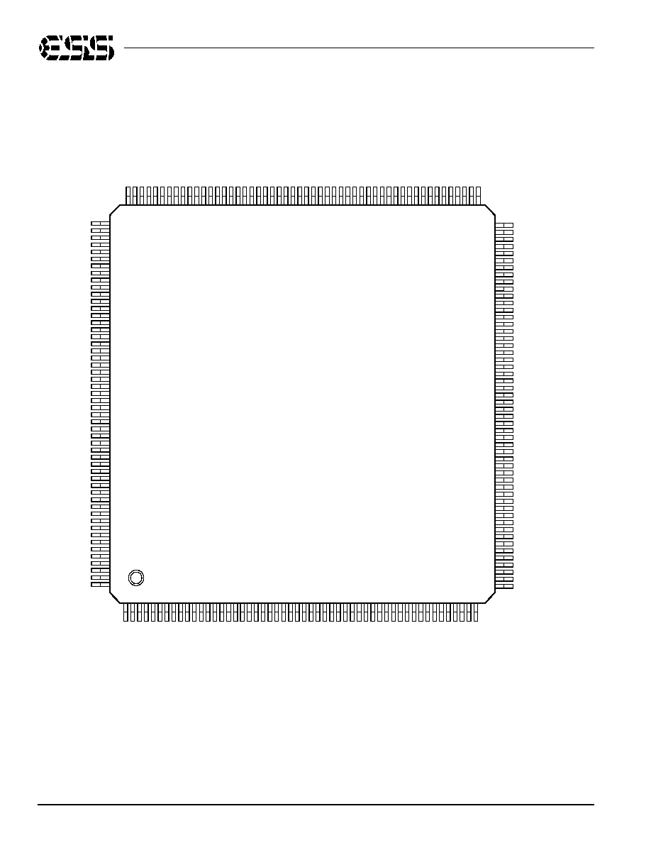
�
Single-chip SVCD decoder in a 208-pin plastic quad flat
package (PQFP)
�
Supports MPEG-1 system and MPEG-2 program streams
�
Programmable multimedia processor architecture
�
Compatible with Audio CD, Video CD 1.1, 2.0, Interactive VCD
3.0, and Super Video CD
Video
�
Trick modes, including Slow, Fast Forward, Fast Reverse, Step,
and Goto
�
4-bit onscreen display (OSD) with 4-bit blending
�
8-bit YUV output
Audio
�
Karaoke function
�
Supports 256/384iframe sync audio system clock
�
Bidirectional I
2
S audio interface
Smart Technology
�
SmartScaleTM for NTSC to PAL conversion and vice versa
�
SmartStreamTM for video error concealment
Peripheral
�
Independent audio bit clock for transmit and receive port
�
Direct servo/loader interface
�
Supports up to 4 MB of SDRAM and/or 4 MB of EDO DRAM
�
Eight general-purpose auxiliary ports
�
Single 27-MHz clock input
�
Power management
BLOCK DIAGRAM
Figure 1 Typical ES4118 System Block Diagram
SwanTM
ES4118
2 MB
SDRAM
CD loader
EPROM
Panel
Interface
NTSC/PAL
Encoder
Audio
Codec
TV
MIC
Speakers
Remote Control/
Keypad
Video
Audio

3
SAM0422-052901
ESS Technology, Inc.
ES4118 PRODUCT BRIEF
ES4118 PIN DESCRIPTION
Table 1 lists the ES4118 pin descriptions.
Table 1 ES4118 Pin Descriptions List
Name
Number
I/O
Definition
VCC
1, 9, 18, 27, 35, 44,
51, 59, 68, 75, 83, 92,
99, 104, 111, 121, 130,
139, 148, 157, 164,
172, 183, 193, 201
I
3.3V power supply.
LA[21:0]
7:2, 16:10, 23:19,
207:204
O
Device address output.
VSS
8, 17, 26, 34, 43, 52,
60, 67, 76, 84, 91, 98,
103, 112, 120, 129,
138, 147, 156, 163,
171, 177, 184, 192,
200, 208
I
Ground.
RESET#
24
I
Reset input, active low.
TDMDX
25
O
TDM transmit data.
RSEL
I
ROM Select.
TDMDR
28
I
TDM receive data.
TDMCLK
29
I
TDM clock input.
TDMFS
30
I
TDM frame sync.
TDMTSC#
31
O
TDM output enable.
TWS
32
O
Audio transmit frame sync.
TSD
33
O
Audio transmit serial data port.
SEL_PLL0
I
Select PLL0:
SEL_PLL2
36
I
Select PLL2. (Refer to the definitions table in pin number 33.)
NC
37, 38, 41, 42,
142:146, 149:155,
158, 202, 203
No connect.
MCLK
39
I/O
Audio master clock for audio DAC.
TBCK
40
I/O
Audio transmit bit clock.
RSD
45
I
Audio receive serial data.
RWS
46
I
Audio receive frame sync.
RBCK
47
I
Audio receive bit clock.
APLLCAP
48
I
Analog PLL capacitor.
XIN
49
I
Crystal input.
XOUT
50
O
Crystal output.
DMA[11:0]
53:58, 61:66
O
DRAM address bus.
DCAS#
69
O
DRAM column address strobe.
DOE#
70
O
DRAM output enable.
DSCK_EN
O
DRAM clock enable
DWE#
71
O
DRAM write enable.
DRAS[2:0]#
74:72
O
DRAM row address strobe.
DB[15:0]
77:82, 85:90, 93:96
I/O
DRAM data bus.
DCS[1:0]#
97, 100
O
SDRAM chip select [1:0], active low.
DQM
101
O
Data input/output mask.
DSCK
102
O
Clock to SDRAM.
RSEL
Selection
0
16-bit ROM
1
8-bit ROM.
SEL_PLL2
SEL_PLL1 SEL_PLL0 Notes
0
0
2.5 x DCLK
0
1
3 x DCLK
1
0
3.5 x DCLK
1
1
4 x DCLK.

4
� 2001 ESS Technology, Inc. All rights reserved.
SAM0422-052901
ES4118 PRODUCT BRIEF
No part of this publication may be reproduced, stored in a
retrieval system, transmitted, or translated in any form or
by any means, electronic, mechanical, manual, optical, or
otherwise, without the prior written permission of ESS
Technology, Inc.
ESS Technology, Inc. makes no representations or
warranties regarding the content of this document.
All specifications are subject to change without prior
notice.
ESS Technology, Inc. assumes no responsibility for any
errors contained herein.
(P) U.S. Patent 4,214,125 and others, other patents
pending.
VideoDrive
�
is a registered trademark of ESS Technology,
Inc.
All other trademarks are owned by their respective
holders and are used for identification purposes only.
ORDERING INFORMATION
DCLK
105
I
Clock input (bypass/test mode).
YUV[7:0]
106:110, 113:115
O
8-bit YUV output.
PCLK2XSCN
116
I/O
27 MHz doubled pixel clock.
PCLKQSCN
117
I/O
13.5 MHz pixel clock.
VSYNC#
118
I/O
Vertical sync.
HSYNC#
119
I/O
Horizontal sync.
HD[15:0]
122:128, 131:137,
140:141
I/O
Host data bus.
VPP
159
I
5V power supply.
AUX[7:0]
160:162, 165:169
I/O
Auxiliary ports.
LOE#
170
O
Device output enable.
LCS[3:0]#
173:176
O
Chip select [3:0].
LD[15:0]
178:182, 185:191,
194:197
I/O
Device data bus.
LWRLL#
198
O
Device write enable.
LWRHL#
199
O
Device write enable.
Table 1 ES4118 Pin Descriptions List (Continued)
Name
Number
I/O
Definition
Part Number
Description
Package
ES4118F
Super VCD Processor
208-pin PQFP