 | –≠–ª–µ–∫—Ç—Ä–æ–Ω–Ω—ã–π –∫–æ–º–ø–æ–Ω–µ–Ω—Ç: 0032 | –°–∫–∞—á–∞—Ç—å:  PDF PDF  ZIP ZIP |
The MSK 0032 is a high speed, FET input, differential amplifier designed to replace the popular LH0032 and
TP0032. Since the MSK 0032 requires less compensation than the LH0032, it exhibits wider bandwidth and greater
stability. The MSK 0032 can be used as a direct replacement in current designs using the LH0032 or TP0032 with no
changes to compensation schemes. High frequency signal transfer circuits such as video amplifiers, high speed
integrators and comparators are just a few of the applications that the MSK 0032 is well suited for.
4707 Dey Road Liverpool, N.Y. 13088
M.S.KENNEDY CORP.
(315) 701-6751
0032
FEATURES:
Fast Slew Rate - 650 V/µS Typ.
FET Input
Wide Bandwidth
Electrically Isolated Case
Industry Wide Pin Compatible 0032 Upgrade
DSCC SMD 5962-80013
DESCRIPTION:
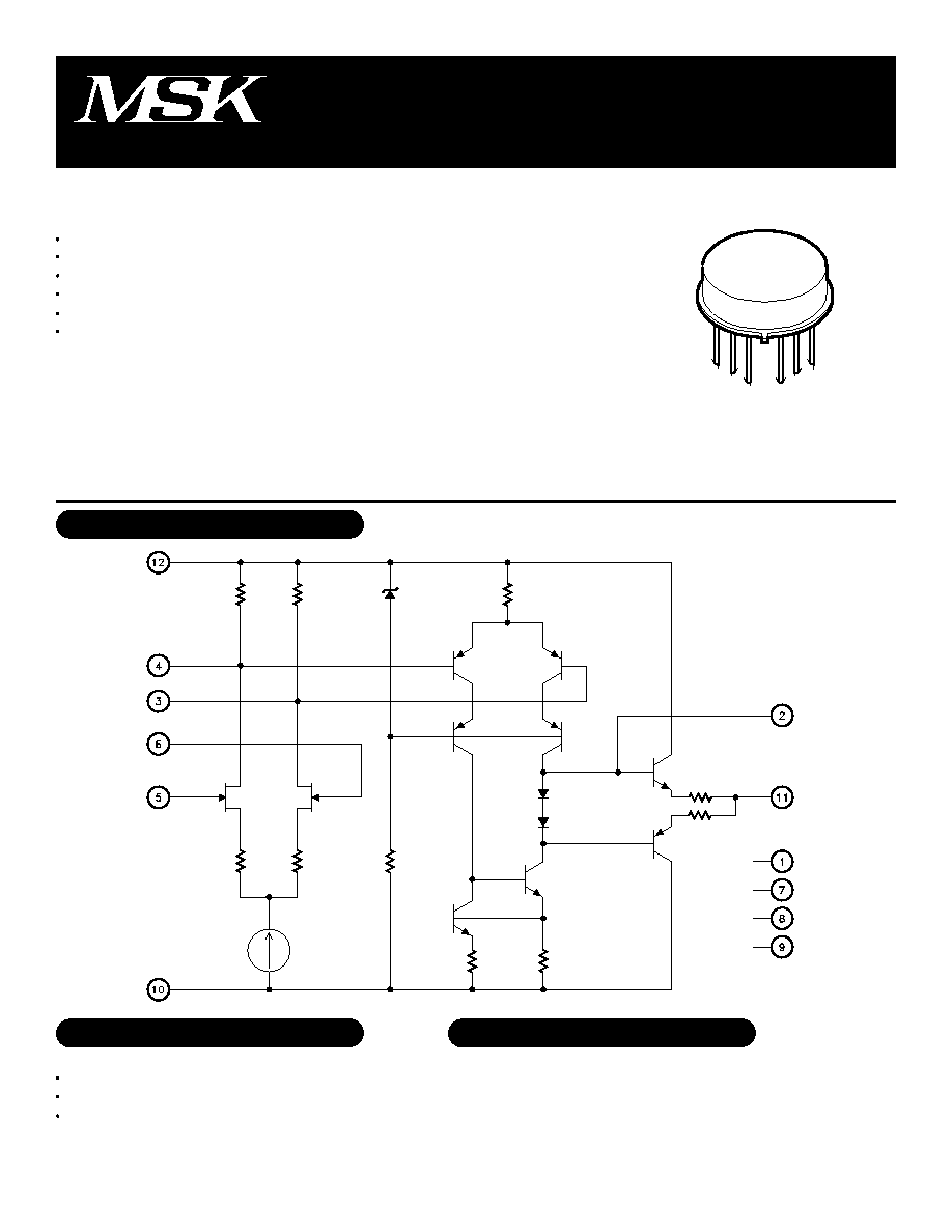
EQUIVALENT SCHEMATIC
No Connection
No Connection
No Connection
Negative Power Supply
Output
Positive Power Supply
1
2
3
4
5
6
No Connection
Output Compensation
Compensation/Balance
Compensation/Balance
Inverting Input
Non-Inverting Input
7
8
9
10
11
12
PIN-OUT INFORMATION
Video Amplifiers
Comparator Circuits
High Speed Integrators
TYPICAL APPLICATIONS
MIL-PRF-38534 CERTIFIED
Rev.B 7/00
1
HIGH SPEED, FET INPUT
DIFFERENTIAL OP-AMP
ISO 9001 CERTIFIED BY DSCC
STATIC
Supply Voltage Range
Quiescent Current
INPUT
Input Offset Voltage
Input Offset Voltage Drift
Input Offset Adjust
Input Bias Current
Input Offset Current
Input Impedance
Power Supply Rejection Ratio
Common Mode Rejection Ratio
Input Noise Voltage
Equivalent Input Noise
OUTPUT
Output Voltage Swing
Output Current
Settling Time to 1%
Settling Time to 0.1%
Unity Gain Bandwidth
TRANSFER CHARACTERISTICS
Slew Rate Limit
Open Loop Voltage Gain
Small Signal Rise Time
Small Signal Delay Time
V
IN
=0V
Bal.Pins=N/C V
IN
=0V A
V
=-10
V/V
Bal.Pins=N/C V
IN
=0V
R
POT
=10K
To +V
CC
V
CM
=0V
Either Input
V
CM
=0V
F=DC
V
CC
=±15V
F=DC V
CM
=±10V
F=10Hz To 1MHz
F=1KHz
R
L
=1K
R
L
=1K
R
L
=1K
10V step
R
L
=1K
10V step
A
V
=+1
V
OUT
=±10V R
L
=1K
V
OUT
=±10V F=100Hz
A
V
= +1 R
L
= 1K
V
IN
= 1V R
L
= 1K
±18V
±40mA
±30V
-55∞C to +125∞C
-40∞C to +85∞C
200∞C/W
ABSOLUTE MAXIMUM RATINGS
T
ST
T
LD
T
J
Storage Temperature Range
Lead Temperature Range
(10 Seconds)
Junction Temperature
-65∞C to +150∞C
300∞C
175∞C
±V
CC
I
OUT
V
IN
T
C
R
TH
1
2
3
4
5
6
7
AV=-1, measured in false summing junction circuit.
Devices shall be capable of meeting the parameter, but need not be tested. Typical parameters are for reference only.
Industrial grade devices shall be tested to subgroups 1 and 4 unless otherwise specified.
Military grade devices ('B' suffix) shall be 100% tested to subgroups 1,2,3 and 4.
Subgroup 5 and 6 testing available upon request.
Subgroup 1,4 T
A
=T
C
=+25∞C
Subgroup 2,5 T
A
=T
C
=+125∞C
Subgroup 3,6 T
A
=T
C
=-55∞C
Electrical specifications are derated for power supply voltages other than ±15VDC.
NOTES:
Supply Voltage
Output Current
Differential Input Voltage
Case Operating Temperature Range
(MSK 0032B)
(MSK 0032)
Thermal Resistance
Junction to Case
Output Devices Only
ELECTRICAL SPECIFICATIONS
±Vcc=±15V Unless Otherwise Specified
Min.
±10
-
-
-
-
-
-
-
-
-
50
50
-
-
±10
±10
-
-
-
350
70
-
-
Max.
±18
±20
±25
±5
±50
±100
±50
25
25
-
-
-
-
-
-
-
0.5
-
-
-
-
20
25
Min.
-
-
-
-
-
-
-
-
-
-
45
45
-
-
±10
±10
-
-
-
350
70
-
-
Max.
±18
±22
-
±7
-
±300
-
100
-
-
-
-
-
-
-
-
0.5
-
-
-
-
20
25
Units
V
mA
mA
mV
µV/∞C
mV
pA
nA
pA
nA
dB
dB
µVrms
nV
Hz
V
mA
µS
nS
MHz
V/µS
dB
nS
nS
MSK 0032B
MSK 0032
2
Typ.
±15
±15
-
±1
-
±25
-
20
-
10
70
80
1.5
40
±12
±20
0.1
300
25
650
-
10
12
Test Conditions
Parameter
1
2
2
7
Typ.
±15
±15
±18
±0.5
±10
±10
±0.2
10
0.1
10
70
80
1.5
40
±12
±20
0.1
300
25
650
-
10
12
Adjust to Zero
Adjust to Zero
12
12
Group A
Subgroup
-
1
2,3
1
2,3
1,2,3
1
2,3
1
2,3
-
-
-
-
-
4
4
4
4
-
4
4
4
4
1
2
2
2
2
Rev.B 7/00
2
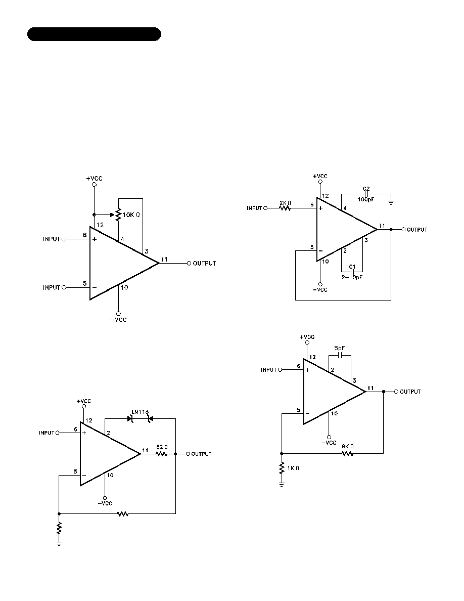
APPLICATION NOTES
HEAT SINKING
Since the case of the MSK 0032 only runs approximately
40∞C hotter than the ambient temperature, a heat sink is gen-
erally not necessary. However, in applications where it is criti-
cal to minimize input bias current, a heat sink may be used.The
case of the MSK 0032 is isolated from the internal circuitry so
the heat sink may be attached directly to the case. The heat
sink may however create enough parasitic capacitance at the
pins to necessitate adjusting the amount of compensation used.
COMPENSATION
When replacing an LH0032 or TP0032 with an MSK 0032,
no changes in compensation need be made. The MSK 0032
will demonstrate greater loop stability than the LH0032 and
loop stability very similar to the TP0032. As with any opera-
tional amplifier, a feedback capacitor in the range of 2-10pF is
recommended to compensate for the effect of the R-C time
constant created by the input capacitance of the op-amp and
the feedback and input resistors in an inverting configuration.
See Figure 3 and Figure 4 for recommended compensation
schemes for non-inverting configurations.
POWER SUPPLY BYPASSING
Both the negative and the positive power supplies must be
effectively decoupled with a high and low frequency bypass
circuit to avoid power supply induced oscillation. An effective
decoupling scheme consists of a 0.1 microfarad ceramic ca-
pacitor in parallel with a 4.7 microfarad tantalum capacitor from
each power supply pin to ground.
The input offset voltage of the MSK 0032 is typically less
than ±0.5mV. If it is necessary to null the offset to zero or
some value other than zero, the above circuit is recommended.
Typical offset adjust range is 25mV.
INPUT OFFSET VOLTAGE NULL
Figure 1
Figure 4
Figure 2
Output Short Circuit Protection
Rev.B 7/00
3
Figure 3
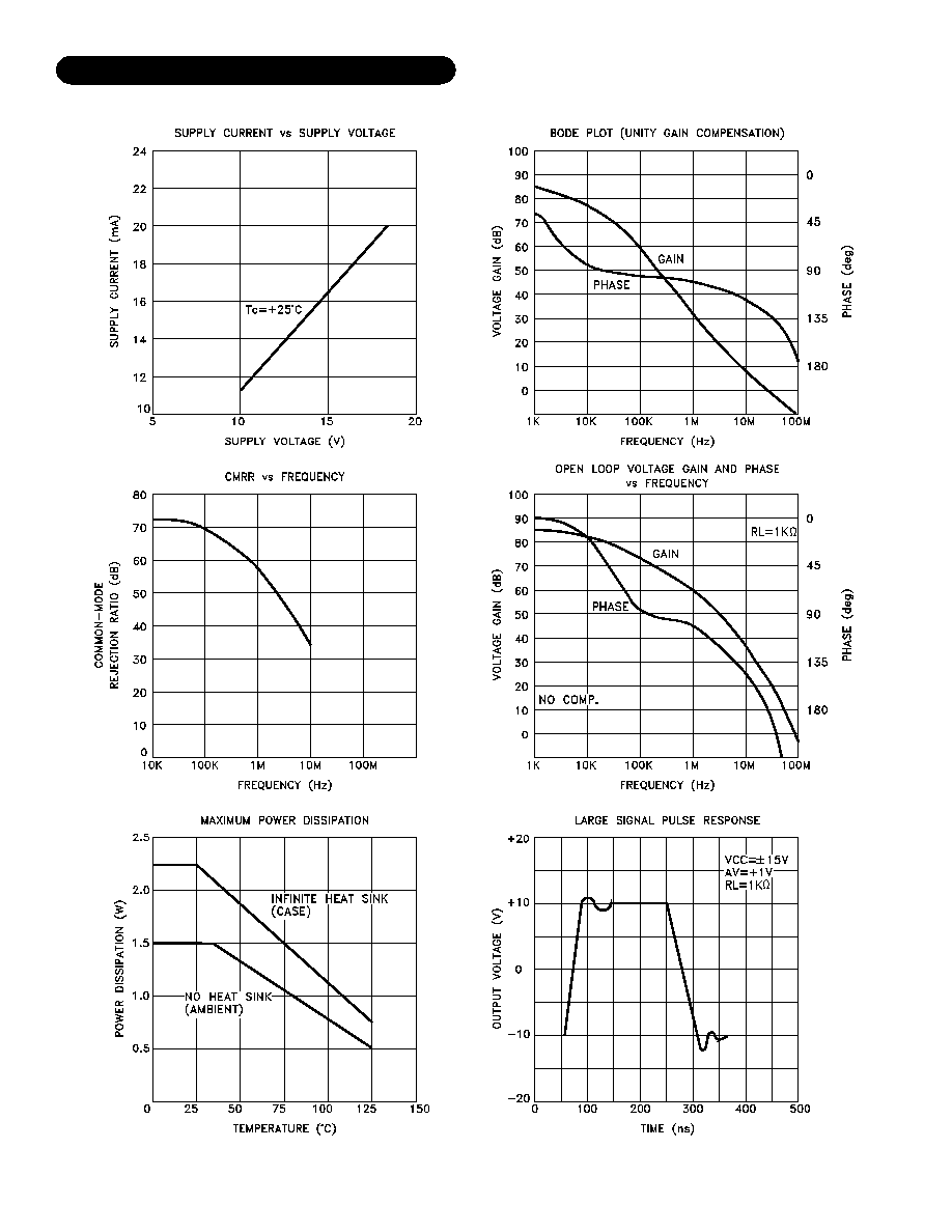
TYPICAL PERFORMANCE CURVES
Rev.B 7/00
4
ORDERING INFORMATION
Screening Level
MSK0032
Industrial
The information contained herein is believed to be accurate at the time of printing. MSK reserves the right to make
changes to its products or specifications without notice, however, and assumes no liability for the use of its products.
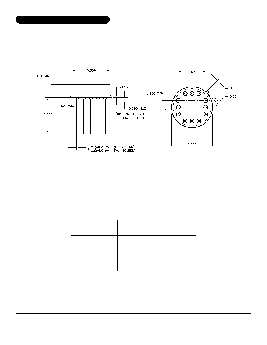
MECHANICAL SPECIFICATIONS
M.S. Kennedy Corp.
4707 Dey Road, Liverpool, New York 13088
Phone (315) 701-6751
FAX (315) 701-6752
www.mskennedy.com
MSK0032B
Part
Number
Rev.B 7/00
5
TO-8 BOTTOM VIEW
ALL DIMENSIONS ARE ±0.010 INCHES UNLESS OTHERWISE LABELED
Military-Mil-PRF-38534
5962-80013
DSCC-SMD