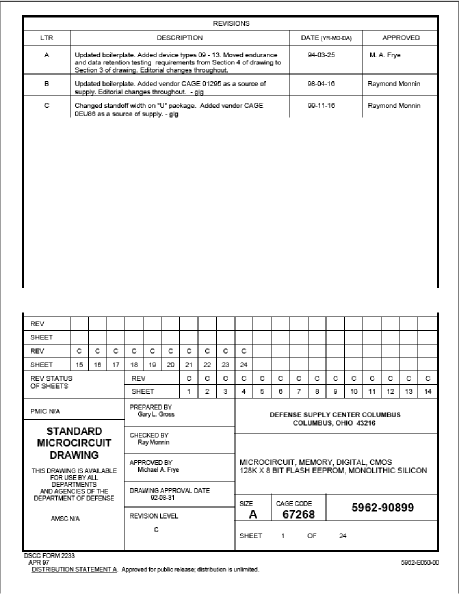
STANDARD
MICROCIRCUIT DRAWING
DEFENSE SUPPLY CENTER COLUMBUS
COLUMBUS, OHIO 43216-5000
SIZE
A
5962-90899
REVISION LEVEL
C
SHEET
3
DSCC FORM 2234
APR 97
1.2.5 Lead finish. The lead finish is as specified in MIL-PRF-38535 for device classes Q and V or MIL-PRF-38535, appendix
A for device class M.
1.3 Absolute maximum ratings. 1/
Endurance:
Device types 01-04, 09 . . . . . . . . . . . . . . . . . . . . . . . . . . . . . . . . . . . . . 10,000 cycles/byte, minimum
Device types 05-08 . . . . . . . . . . . . . . . . . . . . . . . . . . . . . . . . . . . . . . . . 1,000 cycles/byte, minimum
Device types 10-13 . . . . . . . . . . . . . . . . . . . . . . . . . . . . . . . . . . . . . . . . 100,000 cycles/byte, minimum
Supply voltage range (V
) 2/ . . . . . . . . . . . . . . . . . . . . . . . . . . . . . . . . -2.0 V dc to +7.0 V dc
CC
Storage temperature range (T
) . . . . . . . . . . . . . . . . . . . . . . . . . . . . . . -65
C to +150
C
stg
Maximum power dissipation (P ) . . . . . . . . . . . . . . . . . . . . . . . . . . . . . . 1.0 W
D
Lead temperature (soldering, 10 seconds) . . . . . . . . . . . . . . . . . . . . . . . +300
C
Junction temperature (T ) 3/ . . . . . . . . . . . . . . . . . . . . . . . . . . . . . . . . . +150
C
J
Thermal resistance, junction-to-case (
) (case outline X, Y) . . . . . . See MIL-STD-1835
JC
Thermal resistance, junction-to-case (
) (case outlines T, Z) . . . . . . 13
C/W
JC
Thermal resistance, junction-to-case (
) (case outline U) . . . . . . . . . 27
C/W
JC
Voltage on any pin with respect to ground 2/ . . . . . . . . . . . . . . . . . . . . . -2.0 V dc to +7.0 V dc
Voltage on pin A with respect to ground 4/ . . . . . . . . . . . . . . . . . . . . . -2.0 V dc to +13.5 V dc
9
V
supply voltage with respect to ground 4/ . . . . . . . . . . . . . . . . . . . . -2.0 V dc to +14.0 V dc
PP
V
supply voltage with respect to ground 2/ . . . . . . . . . . . . . . . . . . . . -2.0 V dc to +7.0 V dc
CC
Output short circuit current 5/ . . . . . . . . . . . . . . . . . . . . . . . . . . . . . . . . . 200 mA
Data retention . . . . . . . . . . . . . . . . . . . . . . . . . . . . . . . . . . . . . . . . . . . . . 10 years minimum
1.4 Recommended operating conditions. 6/
Supply voltage range (V
) . . . . . . . . . . . . . . . . . . . . . . . . . . . . . . . . . . +4.5 V dc to +5.5 V dc
CC
Operating temperature range (T
) . . . . . . . . . . . . . . . . . . . . . . . . . . . -55
C to +125
C
case
Low level input voltage range (V ) . . . . . . . . . . . . . . . . . . . . . . . . . . . . . -0.5 V dc to +0.8 V dc
IL
High level input voltage range (V
) . . . . . . . . . . . . . . . . . . . . . . . . . . . . +2.0 V dc to V
+0.5 V dc
IH
CC
High level input voltage range, CMOS (V
) . . . . . . . . . . . . . . . . . . . . . . V
-0.5 V dc to V
+0.5 V dc
IH
CC
CC
Chip clear (V ) . . . . . . . . . . . . . . . . . . . . . . . . . . . . . . . . . . . . . . . . . . . . . 11.4 V dc to 12.6 V dc
P
1.5 Digital logic testing for device classes Q and V.
Fault coverage measurement of manufacturing
logic tests (MIL-STD-883, test method 5012) . . . . . . . . . . . . . . . . . . . . 100 percent
1/ Stresses above the absolute maximum rating may cause permanent damage to the device. Extended operation at the
maximum levels may degrade performance and affect reliability.
2/ Minimum dc voltage on input or V pins is -0.5 V. During voltage transitions, inputs may overshoot V
to -2.0 V for
O
SS
periods of up to 20 ns. Maximum dc voltage on output and V pins is V
+0.5 V. During voltage transitions outputs
O
CC
may overshoot to V
+2.0 V for periods up to 20 ns.
CC
3/ Maximum junction temperature shall not be exceeded except for allowable short duration burn-in screening conditions in
accordance with method 5004 of MIL-STD-883.
4/ Minimum dc input voltage on A or V
may overshoot to +14.0 V for periods less than 20 ns.
9
PP
5/ No more than one output shorted at a time. Duration of short circuit should not be greater than 1 second.
6/ All voltages are referenced to V
(ground).
SS
STANDARD
MICROCIRCUIT DRAWING
DEFENSE SUPPLY CENTER COLUMBUS
COLUMBUS, OHIO 43216-5000
SIZE
A
5962-90899
REVISION LEVEL
C
SHEET
4
DSCC FORM 2234
APR 97
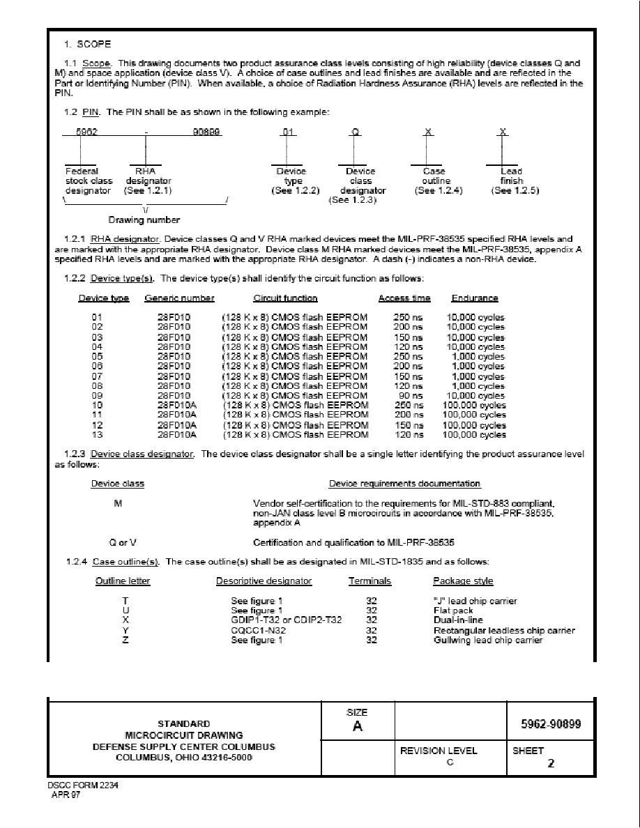
2. APPLICABLE DOCUMENTS
2.1 Government specification, standards, and handbooks. The following specification, standards, and handbooks form a
part of this drawing to the extent specified herein. Unless otherwise specified, the issues of these documents are those listed in
the issue of the Department of Defense Index of Specifications and Standards (DoDISS) and supplement thereto, cited in the
solicitation.
SPECIFICATION
DEPARTMENT OF DEFENSE
MIL-PRF-38535 - Integrated Circuits, Manufacturing, General Specification for.
STANDARDS
DEPARTMENT OF DEFENSE
MIL-STD-883
-
Test Method Standard Microcircuits.
MIL-STD-973
-
Configuration Management.
MIL-STD-1835 -
Interface Standard for Microcircuit Case Outlines.
HANDBOOKS
DEPARTMENT OF DEFENSE
MIL-HDBK-103 -
List of Standard Microcircuit Drawings (SMD's).
MIL-HDBK-780 -
Standard Microcircuit Drawings.
(Unless otherwise indicated, copies of the specification, standards, and handbooks are available from the Standardization
Document Order Desk, 700 Robbins Avenue, Building 4D, Philadelphia, PA 19111-5094).
2.2 Non-Government publications. The following documents form a part of this document to the extent specified herein.
Unless otherwise specified, the issues of the documents which are DoD adopted are those listed in the issue of the DODISS
cited in the solicitation. Unless otherwise specified, the issues of documents not listed in the DODISS are the issues of the
documents cited in the solicitation.
AMERICAN SOCIETY FOR TESTING AND MATERIALS (ASTM)
ASTM Standard F1192-95 - Standard Guide for the Measurement of Single Event Phenomena from
Heavy Ion Irradiation of Semiconductor Devices.
(Applications for copies of ASTM publications should be addressed to the American Society for Testing and Materials,
1916 Race Street, Philadelphia, PA 19103).
ELECTRONICS INDUSTRIES ASSOCIATION (EIA)
JEDEC Standard EIA/JESD78 - IC Latch-Up Test.
(Applications for copies should be addressed to the Electronics Industries Alliance, 2500 Wilson Blvd., Arlington, VA 22201.)
(Non-Government standards and other publications are normally available from the organizations that prepare or distribute
the documents. These documents also may be available in or through libraries or other informational services).
2.3 Order of precedence. In the event of a conflict between the text of this drawing and the references cited herein, the
text of this drawing shall take precedence. Nothing in this document, however, supersedes applicable laws and regulations
unless a specific exemption has been obtained.
STANDARD
MICROCIRCUIT DRAWING
DEFENSE SUPPLY CENTER COLUMBUS
COLUMBUS, OHIO 43216-5000
SIZE
A
5962-90899
REVISION LEVEL
C
SHEET
5
DSCC FORM 2234
APR 97
3. REQUIREMENTS
3.1 Item requirements. The individual item requirements for device classes Q and V shall be in accordance with MIL-PRF-
38535 and as specified herein or as modified in the device manufacturer's Quality Management (QM) plan. The modification in
the QM plan shall not affect the form, fit, or function as described herein. The individual item requirements for device class M
shall be in accordance with MIL-PRF-38535, appendix A for non-JAN class level B devices and as specified herein.
3.2 Design, construction, and physical dimensions. The design, construction, and physical dimensions shall be as
specified in MIL-PRF-38535 and herein for device classes Q and V or MIL-PRF-38535, appendix A and herein for device class
M.
3.2.1 Case outline(s). The case outline(s) shall be in accordance with 1.2.4 herein and figure 1.
3.2.2 Terminal connections. The terminal connections shall be as specified on figure 2.
3.2.3 Truth tables. The truth tables shall be as specified on figure 3.
3.2.3.1 Unprogrammed devices. The truth table for unprogrammed devices for contracts involving no altered item
drawing shall be as specified on figure 3 herein. When required, in screening (see 4.2 herein), or quality conformance
inspection groups A, B, C, or D (see 4.4 herein), the devices shall be programmed by the manufacturer prior to test in a
checkerboard or similar pattern (a minimum of 50 percent of the total number of bits programmed).
3.2.3.2 Programmed devices. The requirements for supplying programmed devices are not part of this document.
3.2.3.3 Command definitions. The command definitions table shall be as specified on figure 3.
3.2.4 Switching test circuits and waveforms. The switching test circuits and waveforms shall be as specified on figure 4.
3.3 Electrical performance characteristics and postirradiation parameter limits. Unless otherwise specified herein, the
electrical performance characteristics and postirradiation parameter limits are as specified in table I and shall apply over the
full case operating temperature range.
3.4 Electrical test requirements. The electrical test requirements shall be the subgroups specified in table IIA. The
electrical tests for each subgroup are defined in table I.
3.5 Marking. The part shall be marked with the PIN listed in 1.2 herein. In addition, the manufacturer's PIN may also be
marked as listed in MIL-HDBK-103. For packages where marking of the entire SMD PIN number is not feasible due to space
limitations, the manufacturer has the option of not marking the "5962-" on the device. For RHA product using this option, the
RHA designator shall still be marked. Marking for device classes Q and V shall be in accordance with MIL-PRF-38535.
Marking for device class M shall be in accordance with MIL-PRF-38535, appendix A.
3.5.1 Certification/compliance mark. The certification mark for device classes Q and V shall be a "QML" or "Q" as required
in MIL-PRF-38535. The compliance mark for device class M shall be a "C" as required in MIL-PRF-38535, appendix A.
3.6 Certificate of compliance. For device classes Q and V, a certificate of compliance shall be required from a QML-38535
listed manufacturer in order to supply to the requirements of this drawing (see 6.6.1 herein). For device class M, a certificate of
compliance shall be required from a manufacturer in order to be listed as an approved source of supply in MIL-HDBK-103 (see
6.6.2 herein). The certificate of compliance submitted to DSCC-VA prior to listing as an approved source of supply for this
drawing shall affirm that the manufacturer's product meets, for device classes Q and V, the requirements of MIL-PRF-38535
and herein or for device class M, the requirements of MIL-PRF-38535, appendix A and herein.
3.7 Certificate of conformance. A certificate of conformance as required for device classes Q and V in MIL-PRF-38535 or
for device class M in MIL-PRF-38535, appendix A shall be provided with each lot of microcircuits delivered to this drawing.
3.8 Notification of change for device class M. For device class M, notification to DSCC-VA of change of product (see 6.2 -
herein) involving devices acquired to this drawing is required for any change as defined in MIL-STD-973.