78P7200
E3/DS3/STS-1
Line Interface Unit
DATA SHEET
Page: 1 of 11
©
2005 Teridian Semiconductor Corporation
Rev 3.0
JULY 2005
DESCRIPTION
The 78P7200 is a line interface transceiver IC
intended for STS-1 (51.84 Mbit/s), DS3 (44.736
Mbit/s) and E3 (34.368 Mbit/s) applications. The
receiver has a very wide dynamic range and is
designed to accept either HDB3 or B3ZS-encoded
Alternate-Mark Inversion (AMI) inputs; it provides
CMOS logic level clock, positive data, negative data
and low-level signal detector outputs. An on-chip
equalizer improves the intersymbol interference
tolerance on the receive path. The transmitter
converts CMOS logic level clock, positive data and
negative data input signals into AMI pulses of the
appropriate shape for transmission. A line buildout
(LBO) equalizer may be selected to shape the
outgoing pulses for shorter line lengths. The
78P7200 requires a single 5 volt supply and is
available in a surface mount package.
FEATURES
∑
Single chip transmit and receive interface for
STS-1 (51.84 Mbit/s), E3 (34.368 Mbit/s) or DS3
(44.736 Mbit/s) applications
∑
On-chip Receive Equalizer
∑
Unique clock recovery circuit, requires no
crystals, tuned components or external clock
∑
Selectable transmit line buildout (LBO) to
accommodate shorter line lengths
∑
Compliant with ANSI T1.102-1993, Bellcore TR-
NWT-000499 and GR-253-CORE, ITU-T G.703
and G.823_1991
∑
Low-level input signal indication
∑
Available in a 28 PLCC surface mount package
∑
-40∞C to +85∞C operating range
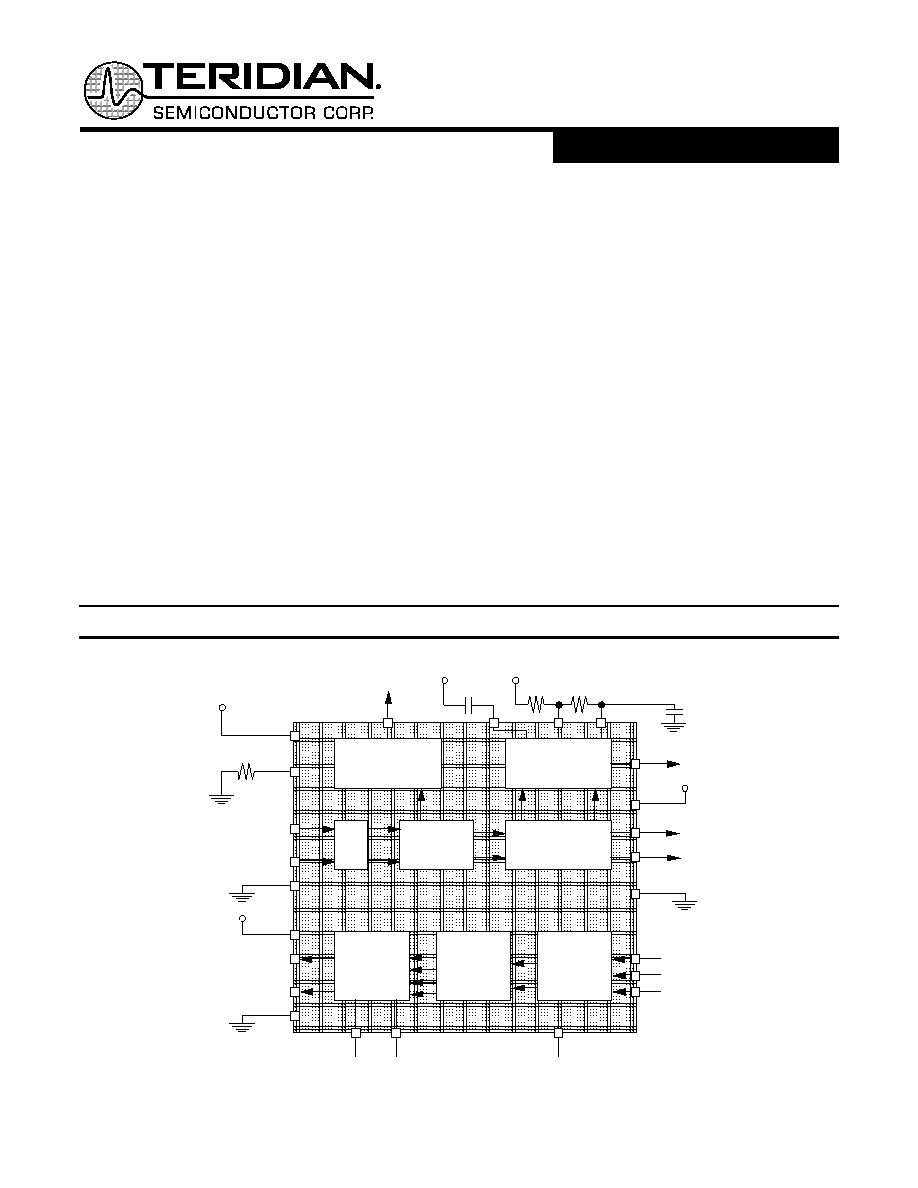
BLOCK DIAGRAM
Low-Level Signal
Detection
Clock Recovery
Data
Detection
RVcc
RFO
TVcc
OPT!
TCLK
TPOS
TNEG
DGND
RNEG
RPOS
DVcc
RCLK
LOWSIG
RLF2
Signal
Acquisition
Output
Driver,
Line
Buildout
OPT@
RLF1
LBO
Pulse
Shaper
Pulse
Generator
CLF1
RVcc
Eq.
RVcc
CPD
INPUT
OUTPUT
LIN+
LIN-
LOUT+
LOUT-

78P7200
E3/DS3/STS-1
Line Interface Unit
Page: 2 of 11
©
2005 Teridian Semiconductor Corporation
Rev 3.0
FUNCTIONAL DESCRIPTION
The 78P7200 is a single chip line interface IC
designed to work with either a 51.84 Mbit/s STS-1,
44.736 Mbit/s DS3 or 34.368 Mbit/s E3 signal. The
receiver recovers clock, positive data and negative
data from an Alternate Mark Inversion (AMI) signal.
The input signal should be B3ZS or HDB3 coded.
The transmitter accepts CMOS level logical clock,
positive data and negative data and converts them
to the AMI signal to drive a 75
coaxial cable.
Programmable internal Line Buildout (LBO) circuitry
eliminates the need for external LBO networks.
When the option pins are properly selected, the
shape of the transmitted signal through any cable
length of 0 to 450 feet complies with the published
templates of ANSI T1.102, ITU-T G.703, Bellcore
TR-NWT-000499 and GR-253-CORE. The 78P7200
is designed to work with a B3ZS or HDB3 coded
signal. The B3ZS or HDB3 encoding and decoding
functions are normally included in the framer ICs or
can easily be implemented in a PAL.
RECEIVER
The receiver input is normally transformer-coupled to
the AMI signal. The inputs to the IC are internally
referenced to RVCC. Since the input impedance of
the 78P7200 is high, the AMI line must be
terminated in 75
. The input signal to the 78P7200
must be limited to a maximum of three consecutive
zeros using a coding scheme such as B3ZS or
HDB3.
The AMI signal first enters a fixed equalizer, which is
designed to overcome the intersymbol interference
caused by long cable lengths and crosstalk. This
fixed equalizer is optimized for DS3 application and
its effect should be compensated by an external filter
circuit similar to Figure 1, for all square shaped
signals such as DS3-high or 34 Mbit/s E3. For all
new designs, the addition of the filter for DS3 and
STS-1 as well as E3 rate allows the circuit to work
with sharp pulses such as DS3-high. The signal is
then input to a variable gain differential amplifier
whose output is maintained at a constant voltage
level regardless of the input voltage level. The gain
of this amplifier is adjusted by detecting the peak of
the signal and comparing it to a fixed reference.
The output of the variable gain amplifier is compared
to a threshold value, which is a fixed percentage of
the signal peak. In this way, even though the input
signal amplitude may fall below the minimum value
that can be regulated by the variable gain circuit, the
proper detection threshold is maintained.
Outputs of the data comparators are connected to
the clock recovery circuits. The clock recovery
system employs a unique phase locked loop, which
has an auxiliary frequency-sensitive acquisition loop,
which becomes active only when cycle-slipping
occurs between the received signal rate and the
internal oscillator.
This system permits the loop to independently lock
to the frequency and phase of the incoming data
stream without the need for high precision and/or
adjustable oscillator or tuned circuits.
The frequency characteristic for the phase locked
loop is established by external filter components,
RLF1, RLF2 and CLF1. The values of these
components are specified such that the bandwidth of
the phase locked loop is greater than 200 kHz.
The jitter tolerance of the 78P7200 exceeds the
requirements of TR-NWT-000499 for Category II
equipment for DS3 rate and exceeds the
requirements of ITU-T G.823 for E3 rate. The jitter
transfer function is maximally flat so the IC doesn't
add any significant jitter to the system.
Figure 2 shows the recovered clock (RCLK), positive
data (RPOS) and negative data (RNEG) signals
timing. The data is valid on the rising edge of the
clock. The minimum setup and hold times allow easy
interface to framer circuits. These signals are
CMOS-level outputs.
Should the input signal fall below a minimum value,
the
LOWSIG
pin goes active low. A time delay is
provided before this output is active so that transient
interruptions do not cause false indications. This
signal should be used as one of many indications to
the cable disconnect; the framer device should count
the number of zeros to declare the loss of signal.
The RPOS and RNEG signals generate random
data following a silence period. The framer device
should ignore RPOS and RNEG data if the
LOWSIG
pin is active low.
78P7200
E3/DS3/STS-1
Line Interface Unit
Page: 3 of 11
©
2005 Teridian Semiconductor Corporation
Rev 3.0
TRANSMITTER
The transmitter accepts CMOS logic level clock
(TCLK), positive data (TPOS) and negative data
(TNEG) signals and generates high current drive
pulses on the LOUT+ and LOUT- pins. When
properly connected to a center tapped transformer,
an AMI pulse is generated which can drive a 75
coaxial cable.
Figure 3 shows the timing for the transmitter logic
signals. The output pulse width is internally set and
is not sensitive to input clock (TCLK) pulse width.
When a recommended transformer is used and
option pins are properly set, the transmitted pulse
shape at the end of a 75
terminated cable of 0 to
450 feet will fit the template for DSX3 pulse
published in ANSI T1.102-1993, Bellcore
TR-NWT-000499 documents.
For 51.84 Mbit/s STS-1 application the transmitted
pulse for a short cable meets the requirements of
Bellcore GR-253-CORE. For 34 Mbit/s E3
application, the transmitted pulse for a short cable
meets the requirements of ITU-T G.703 when both
LBO and
OPT!
pins are set LOW.
The 78P7200 incorporates a selectable Line
Buildout (LBO) pulse shaper in the transmitter path.
For STS-1 and DS3 applications, the LBO pin
should be set HIGH if the cable is shorter than 225
feet and set LOW for longer cable lengths. For E3
application, LBO pin should be set LOW regardless
of cable length.
The
OPT!
pin is set HIGH for DS3 and STS-1
operation. The
OPT!
pin should be set LOW for E3
applications.
The
OPT@
pin should be set HIGH for normal
operation. By setting the
OPT@
pin to LOW it disables
the transmitter drivers and reduces the power
consumption of the circuit by approximately 125 mW.
Recommended settings for
OPT!
and LBO pins
SPEED CABLE
OPT!
OPT!
OPT!
OPT!
LBO
DS3/STS1 <
225'
HI
HI
DS3/STS1 >
225'
HI
LOW
E3 ALL LOW
LOW
OPT!
OPT!
OPT!
OPT!
78P7200
E3/DS3/STS-1
Line Interface Unit
Page: 4 of 11
©
2005 Teridian Semiconductor Corporation
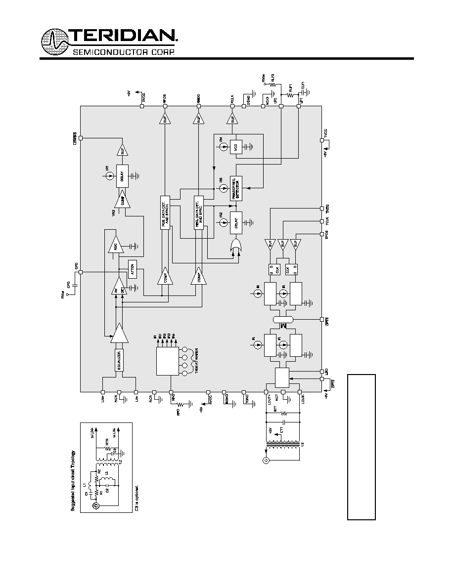
Rev 3.0
VR1
AMP
PULSE
GEN.
PULSE
GEN.
VAR
AMP
GAIN
REFERENCE
CURRENT
GENERATOR
OUTPUT
DRIVER
PULSE
SHAPER 2
PULSE
SHAPER 1
N
o
te:
N
C
pins
sho
uld
be t
ied
to t
he
ground
pin i
ndi
cat
ed b
y
th
e tra
ili
ng l
e
tt
er.
FIGURE
1
:
Func
tiona
l Dia
g
r
a
m
78P7200
E3/DS3/STS-1
Line Interface Unit
Page: 5 of 11
©
2005 Teridian Semiconductor Corporation
Rev 3.0
PIN DESCRIPTION
RECEIVER
NAME TYPE
DESCRIPTION
LIN+, LIN-
I
Differential inputs, transformer-coupled from coax cable.
RPOS
O
Unipolar receiver output, active as result of positive pulse at inputs.
RNEG
O
Unipolar receiver output, active as result of negative pulse at inputs.
RCLK
O
Recovered Clock from line data.
LOWSIG
O
Low signal logic output indicating that input signal is less than threshold value.
TRANSMITTER
TPOS
I
Unipolar transmitter data input, active high.
TNEG
I
Unipolar transmitter data input, active high.
TCLK
I
Transmitter clock input, active high.
LOUT+
O
Output to transformer for positive data pulses.
LOUT-
O
Output to transformer for negative data pulses.
LBO
I
Transmitter line buildout control. Set low for all E3 or for DS3/STS-1 cable of 225'
or longer. Set high for short DS3/ STS-1 cable.
OPT!
I
Transmit option 1. Set high for DS3/STS-1 and set low for E3.
OPT@
I
Transmit option 2. Disables output driver and reduces output bias current when
low. Set high for normal transmit operation.
EXTERNAL COMPONENT CONNECTION
RFO
I
Resistor connected to RGND adjusts the center frequency of receiver phase
locked loop oscillator and the transmitter pulse width and amplitude.
LF1, LF2
-
Resistor-capacitor loop filter network to establish bandwidth of phase locked loop.
CPD
-
Capacitor to RVcc that is connected to peak detector node to reduce signal-
dependent ripple on that node.
POWER
TVcc
-
5V power supply for transmit circuits.
RVcc
-
5V power supply for receive circuits.
DVcc
-
5V power supply for receive logic circuits.
TGND
-
Ground return for transmit circuits.
RGND
-
Ground return for receive circuits.
DGND
-
Ground return for receive logic circuits.
NCR
-
No connect, Tie to Receiver Ground (RGND).
NCT
-
No connect, Tie to Transmitter Ground (TGND).
NCD
-
No connect, Tie to Digital Ground.