FireLink USB
82C862/863
912-2000-030
Page i
Revision: 1.1
Æ
T
ABLE
OF
C
ONTENTS
1.0
FEATURES ......................................................................................................................................................................1
1.1
O
VERVIEW
.......................................................................................................................................................... 1
2.0
SIGNAL DEFINITIONS ....................................................................................................................................................3
2.1
T
ERMINOLOGY
/N
OMENCLATURE
C
ONVENTIONS
................................................................................................................... 3
2.2
N
UMERICAL
P
IN
C
ROSS
-R
EFERENCE
L
IST
........................................................................................................................... 5
2.3
S
IGNAL
D
ESCRIPTIONS
...................................................................................................................................................... 6
2.3.1
Clock and Reset Interface Signals ....................................................................................................................... 6
2.3.2
PCI Bus Interface Signals..................................................................................................................................... 6
2.3.3
USB Interface Signals .......................................................................................................................................... 9
2.3.4
Host Controller shared signals: PME#, SMI#, REQ#, GNT# ................................................................................ 9
2.3.5
Legacy and Interrupt Interface Signals ............................................................................................................... 10
2.3.6
Power and Ground Pins ..................................................................................................................................... 10
2.3.7
Strap Options ..................................................................................................................................................... 11
3.0
FUNCTIONAL DESCRIPTION.......................................................................................................................................13
3.1
U
NIVERSAL
S
ERIAL
B
US
(USB) ........................................................................................................................................ 13
3.2
PCI C
ONTROLLER
........................................................................................................................................................ 14
3.3
C
LOCK
G
ENERATION
....................................................................................................................................................... 15
3.4
P
OWER
M
ANAGEMENT
F
EATURES
.................................................................................................................................... 15
3.4.1
Putting FireLink into USBSuspend State ............................................................................................................ 15
3.4.2
Powering Down the USB I/O Cells ..................................................................................................................... 15
3.4.3
Stopping the 48MHz USB Clock......................................................................................................................... 15
3.4.4
Using CLKRUN# ................................................................................................................................................ 15
3.4.5
Stopping the Internal USB Clocks ...................................................................................................................... 16
3.4.6
Power Control Modes ......................................................................................................................................... 16
3.5
H
OST
C
ONTROLLER
........................................................................................................................................................ 19
3.5.1
Legacy Support .................................................................................................................................................. 20
3.5.2
Intercept Port 60h and 64h Accesses................................................................................................................. 20
3.6
G
ENERAL
P
URPOSE
P
INS
................................................................................................................................................ 21
4.0
REGISTER DESCRIPTIONS .........................................................................................................................................23
4.1
PCICFG R
EGISTER
S
PACE
............................................................................................................................................. 23
4.1.1
Programming Differences from 82C861 Component.......................................................................................... 23
4.1.2
PCICFG 00h-FFh ............................................................................................................................................... 24
4.2
H
OST
C
ONTROLLER
R
EGISTER
S
PACE
.............................................................................................................................. 29
4.2.1
MEMOFST 00h-5Ch........................................................................................................................................... 29
4.2.2
Legacy Support Registers .................................................................................................................................. 39
4.2.3
MEMOFST 100h-1Fh (Legacy Support Registers)............................................................................................. 39
5.0
ELECTRICAL RATINGS................................................................................................................................................41
5.1
A
BSOLUTE
M
AXIMUM
R
ATINGS
......................................................................................................................................... 41
5.2
DC C
HARACTERISTICS
: ................................................................................................................................................... 41
5.3
AC C
HARACTERISTICS
(P
RELIMINARY
).............................................................................................................................. 42
5.3.1
PCI Bus AC Timings........................................................................................................................................... 42
5.3.2
USB AC Timings: Full Speed Source ................................................................................................................. 43
5.3.3
USB AC Timings: Low Speed Source ................................................................................................................ 44
6.0
MARKING AND ORDER INFORMATION .....................................................................................................................46
6.1
P
ACKAGE
M
ARKING
........................................................................................................................................................ 46
6.2
O
RDER
N
UMBER AND
S
HIPPING
B
OX
I
NFORMATION
............................................................................................................ 47
6.3
P
ACKAGE
S
PECIFICATIONS
.............................................................................................................................................. 47
7.0
MECHANICAL PACKAGE OUTLINES .........................................................................................................................48
8.0
NAND TREE TEST MODE.............................................................................................................................................49
FireLink USB
82C862/863
912-2000-030
Page 1
Revision: 1.1
Æ
1.0 Features
The OPTi 82C862 and 82C863 FireLink USB devices are
high performance USB host controllers. Both products
share the same dual transfer engine design, the only
difference being that the 82C862 product implements four
USB ports, while the 82C863 product implements two
ports.
Their shared feature set is as follows.
∑
Compliant with USB rev. 1.1 specification
∑
Compliant with PCI rev 2.2 specification
∑
Implements complete USB Open Host Controller
Interface (OHCI) specification
∑
Two independent host controllers (implemented as a
multi-function PCI device)
∑
Two USB ports (82C862) or one USB port (82C863) per
controller
∑
Second host controller can be disabled if not used to
save power
∑
Clock input can be derived from either a 12MHz crystal
or a 48MHz oscillator
∑
Clocks can be turned off when not in use to save power
∑
Core operates at 3.3V; PCI inputs are 5V-tolerant
∑
Incorporates PCI Power Management, supporting very
low power standby modes
∑
Implements CLKRUN# pin to support hardware-
enforced power-down
∑
Packaged as 100-pin LQFP (Low-profile Quad Flat
Pack)
∑
Supported by Windows 98, Windows Me, Windows
2000, Windows XP, Windows CE, Apple Mac OS, Linux
1.1
Overview
This document describes the OPTi FireLink USB
82C862/82C863 controller.
This PCI-to-USB bridge is unique in that it consists of two
independent dual-port controllers, each sharing only the
common PCI bus connection. This arrangement allows for
a total Universal Serial Bus bandwidth of 24Mbps, divided
into 12Mbps for each pair of ports (or 12Mbps per port in
the case of the 82C863).
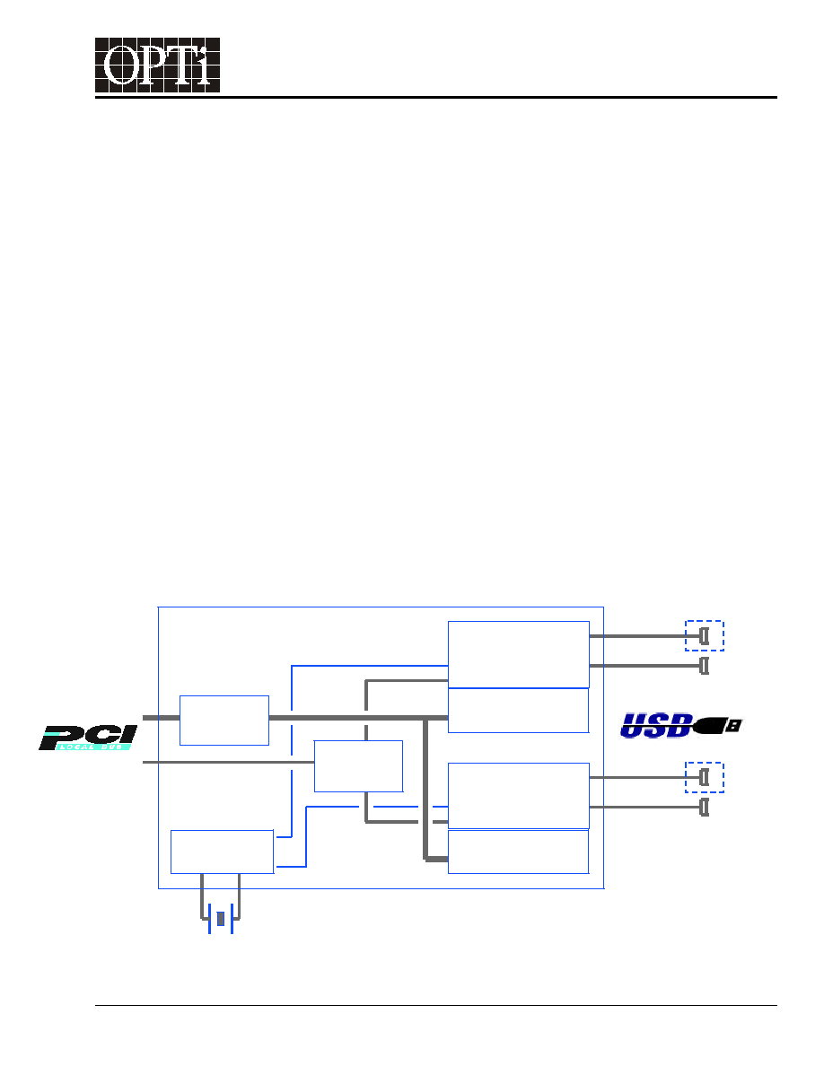
Figure 1 provides a block diagram of the overall
functionality of the chip.
Figure 1.
FireLink USB Block Diagram
port 2
12MHz
xtal
USB
Controller
Module 1
FireLink
FireLink
USB
82C862/3
PCI
interface
48MHz Clock
Generation
Central
Arbiter
USB Config Regs
Function 0
USB
Controller
Module 2
USB Config Regs
Function 1
port 1
port 4
port 3
REQ#, GNT#
82C862
only
82C862
only