 | –≠–ª–µ–∫—Ç—Ä–æ–Ω–Ω—ã–π –∫–æ–º–ø–æ–Ω–µ–Ω—Ç: B1584 | –°–∫–∞—á–∞—Ç—å:  PDF PDF  ZIP ZIP |
Bay Linear, Inc
2478 Armstrong Street, Livermore, CA 94550 Tel: (925) 989-7144, Fax: (925) 940-9556 www.baylinear.com
8.0A Low Dropout Voltage Regulator
B1584
Adjustable & Fix Output
Advance Information
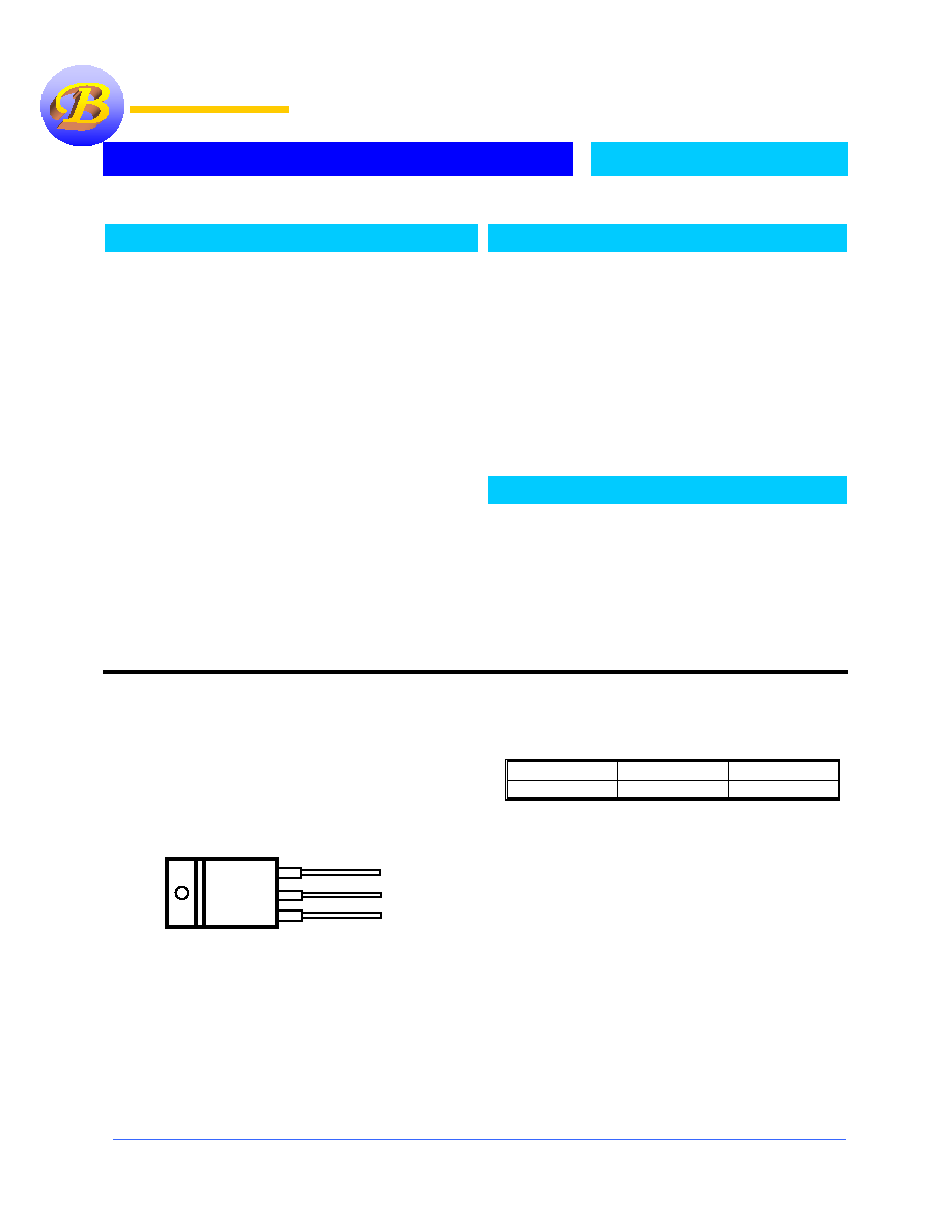
Pin Connection
Ordering Information
Devices Package Temp.
B1584T TO-220
0
∞
C to 70
∞
C
Description
The Bay Linear B1584 is Monolithic low power 8.0A
Adjustable and fixed NPN voltage regulator that are easy to
use with minimum external components. It is suitable for
applications requiring a well-regulated positive output voltage
with low input-output differential voltage requirements and
output voltage 1.5V, 2.5V, 3.0V, 3.3V, or 5V.
The B1584 Outstanding features include full power usage up
to 8.0Amp of load current internal current limiting and thermal
shutdown. Other fixed versions are also available consult with
factory.
The B1584 is offered in 3-pin TO-220 & TO-263 packages
compatible with other 3 terminal regulators. For 5A Low
dropout Regulator refer to the B1585 data sheet.
Features
∑
Adjustable Output Down to 1.2V
∑
Fixed Output Voltages 2.5V, 3.0V 3.3V,
and 5.0V
∑
Output Current of 8.0A
∑
Low Dropout Voltage 1.1V Typ.
∑
Current & Thermal Limiting
∑
Standard 3-Terminal Low Cost TO-220
∑
Similar to industry Standard
LT1083/LT1584
Applications
∑
3.3V to 2.5V for Pentium Processor
∑
SMPS Post Regulator
∑
High Efficiency "Green" Computer
Systems
∑
High Efficiency Linear Power Supplies
∑
5V to 3.XXV fro Pentium Processor
∑
Battery Charger
Bay Li
Bay Li
Bay Li
Bay Linear
near
near
near
Linear Excellence
Linear Excellence
Linear Excellence
Linear Excellence
Plastic Package
TO-220
Front View
V
OUT
GND
V
IN
Plastic Package
TO-220
Plastic Package
TO-220
Front View
V
OUT
V
OUT
GND
V
IN
V
IN

Bay Linear, Inc
2478 Armstrong Street, Livermore, CA 94550 Tel: (925) 989-7144, Fax: (925) 940-9556 www.baylinear.com
B1584
Absolute Maximum Rating
Parameter Symbol
Value
Unit
Maximum Input Voltage
V
IN
7 V
Power Dissipation
P
O
Internally Limited
W
Thermal Resistance Junction to Case
JC
3
Thermal Resistance Junction to
Ambient
JA
50
∞
C/W
Operating Junction
Temperature Range
Control Section
Power Transistor
T
J
0 to 125
0 to 150
Storage Temperature Range
T
STG
-65 to 150
Lead Temperature (Soldering 10
Sec.)
T
LEAD
260
∞
C
Electrical Characteristics
(V
IN
= 4.75V to 5.25V; I
O
= 10mA to 8.0Amp, unless otherwise specified)
Parameter Symbol
Conditions
MIN
TYP
MAX
UNIT
1.485 1.515
0<I
OUT
<5A, 3.3V<V
IN
<7V, T= 25
∞
C
0<I
OUT
<5A, 3.3V<V
IN
<7V, Over Temp.
1.475
1.5
1.525
2.475 2.525
0<I
OUT
<5A, 4.0V<V
IN
<7V, T= 25
∞
C
0<I
OUT
<5A, 4.0V<V
IN
<7V, Over Temp.
2.460
2.5
2.540
2.970 3.030
0<I
OUT
<5A, 4.5V<V
IN
<7V, T= 25
∞
C
0<I
OUT
<5A, 4.5V<V
IN
<7V, Over Temp.
2.950
3.0
3.050
3.267 3.333
0<I
OUT
<5A, 4.8V<V
IN
<7V, T= 25
∞
C
0<I
OUT
<5A, 4.8V<V
IN
<7V, Over Temp.
3.247
3.3
3.353
4.950 5.050
Output Voltage
V
O
0<I
OUT
<5A, 6.5V<V
IN
<7V, T= 25
∞
C
0<I
OUT
<5A, 6.5V<V
IN
<7V, Over Temp.
4.920
5.0
5.080
V
1.238 1.262
Reference Voltage
V
ref
V
IN
<7V, 1.5V<V
IN
<5.75, 10mA<I
out
<5Amp
1.230
1.250
1.270
V
Line Regulation (1)
REG
(line)
I
O
= 10mA, V
IN
=5V, T= 25
∞
C
0.04
0.2
0.08 0.40
Load Regulation (1)
REG
(LOAD)
I
O
= 10mA, V
IN
=5V, T= 25
∞
C
%
1.0
Dropout Voltage
V
D
T= 25
∞
C
Over Temperature
1.1 1.3
V
Minimum load Current
I
min
5.0
10
mA
Current Limit
I
S
(V
in
-V
out
)=3V 8
10
A
Ground Pin Current
I
Q
V
IN
=5V
0
200
mA
Temperature Stability
T
S
I
O
= 10mA, V
IN
=5V
0.5
%
Thermal Regulation
T= 25
∞
C, 30ms pulse
0.003 %/W
Ripple Rejection
R
A
T= 25
∞
C, V
IN
=5V
60 80 dB
Thermal Resistance
-
TO-220 Junction to Tab
Junction to Ambient
DD Package Junction to Tab
Junction to Ambient
3.0
60
3.0
60
3.0
60
3.0
60
∞
C/W
Note: Output Switch tests are performed under pulsed conditions to minimize power dissipation

Bay Linear, Inc
2478 Armstrong Street, Livermore, CA 94550 Tel: (925) 989-7144, Fax: (925) 940-9556 www.baylinear.com
Advance Information- These data sheets contain descriptions of products that are in development. The specifications are based on the engineering calculations,
computer simulations and/ or initial prototype evaluation.
Preliminary Information- These data sheets contain minimum and maximum specifications that are based on the initial device characterizations. These limits are
subject to change upon the completion of the full characterization over the specified temperature and supply voltage ranges.
The application circuit examples are only to explain the representative applications of the devices and are not intended to guarantee any circuit
design or permit any industrial property right to other rights to execute. Bay Linear takes no responsibility for any problems related to any
industrial property right resulting from the use of the contents shown in the data book. Typical parameters can and do vary in different
applications. Customer's technical experts must validate all operating parameters including " Typical" for each customer application.
LIFE SUPPORT AND NUCLEAR POLICY
Bay Linear products are not authorized for and should not be used within life support systems which are intended for surgical
implants into the body to support or sustain life, in aircraft, space equipment, submarine, or nuclear facility applications without
the specific written consent of Bay Linear President.