Bay Linear, Inc
2418Armstrong St., Livermore CA USA 94550 Tel: (925) 606-5950, Fax: (925) 940-9556 www.baylinear.com
Dual USB High Side Power Switch
B2526
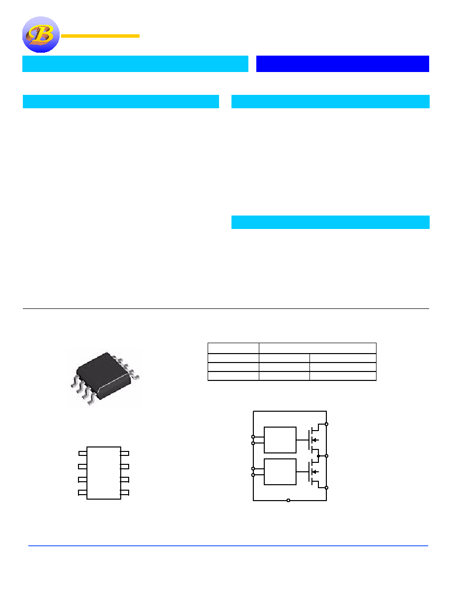
Package Information
Ordering Information
Package Enable
Active High
Active Low
SO-8 B2526-1M
B2526-2M
8 DIP
B2526-1P
B2526-2P
Description
The Bay Linear B2526 is a dual high-side power switch
recommended for self-powered and bus-powdered universal
serial for bus (USB) application conforming to USB
requirements. USB voltage drop requirements, fault current
limited to 750mA, flag output to indicate fault connections to
the local USB controller are features that meet USB
requirements.
Additional features such as thermal shutdown to prevent
catastrophic switch failure from excessively high current
loads, under voltage lockout (UVLO) to ensure that the device
remains off unless there is a valid input voltage present, and
3.3V or 5V logic compatible enable inputs. Two versions of
the enable pin, Active High or Active Low are available in 8-
pin Dip and 8-pin SOIC packages.
Features
�
3.0V to 5.5V Input
�
110
�
�
�
�
A Typical on-State Supply Current
�
1
�
�
�
�
A Typical off-State Supply Current
�
500mA Minimum Continuous Load Current
�
1.25A Maximum Current Limit
�
2.4V Typical Under Voltage Lockout (UVLO)
�
Open-Drain Fault Flag Pin
�
Thermal Shutdown
�
Available with Active-High or Active-Low Enable
Applications
�
USB Host and self-Powered Hubs
�
USB Power Management
�
Battery-Charger Circuits
�
Hot Plug-In Power Supplies
�
Bus-Powered Hubs
Bay Linear
Bay Linear
Bay Linear
Bay Linear
Inspire the Linear Power
Inspire the Linear Power
Inspire the Linear Power
Inspire the Linear Power
Top View
2
1
3
4
8
7
6
5
BAY
B2526
FLAG (B)
EN (B)
V
OUT
(A)
GND
V
IN
FLAG (A)
EN (A)
SO-8
V
OUT
(B)
Logic
Charge
Pump
Logic
Charge
Pump
8 Out (A)
7 IN
5 Out (B)
6 GND
EN (A) 1
FLG (A) 2
FLB (B) 3
EN (B) 4
Bay Linear, Inc
2418Armstrong St., Livermore CA USA 94550 Tel: (925) 606-5950, Fax: (925) 940-9556 www.baylinear.com
B2526
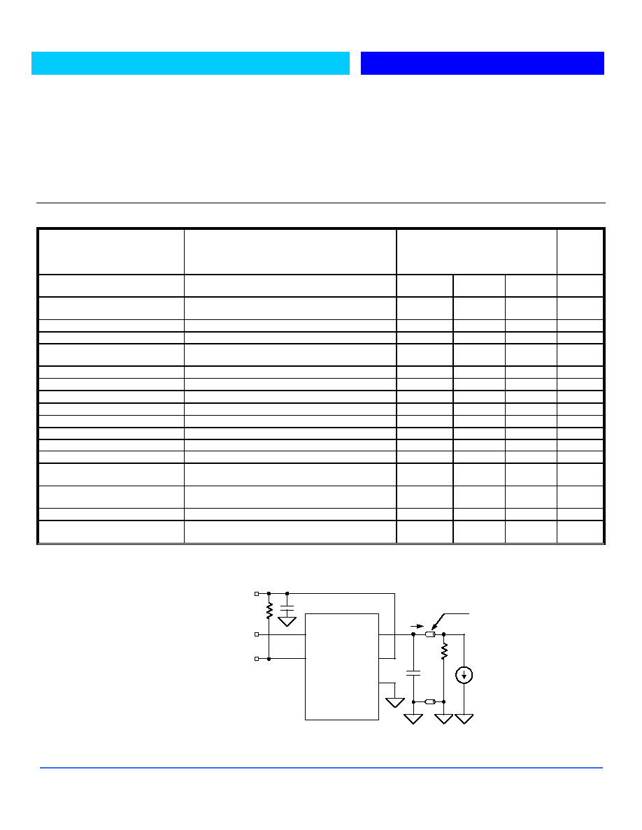
ABSOLUTE MAXIMUM RATINGS OPERATING RATING
Supply Voltage..........................................6V
Supply Voltage ..................................................+3V to +5.5V
Fault Flag Voltage......................................6V
Ambient Operating Temperature.................... -40
�
C to +85
�
C
Fault Flag Current...................................50mA
Output Voltage..........................................6V
Output Current........................Internally Limited
Enable Input.................................-0.3V to 12V
Storage Temperature..................-65
�
C to +150
�
C
Lead Temperature (Soldering 5 sec.).............260
�
C
Thermal
Resistance
SOIC.................................................................. 120
�
C/W
DIP..................................................................... 130
�
C/W
ELECTRICAL CHARACTERISTICS
at V
IN
= 5V, Ta=25
�
C, unless otherwise specified. (Note 1)
Parameters
Conditions
Typ
Min
Max
Units
Supply Current
(Note1) Switch Off, OUT = Open
(Note1) Switch On, OUT = Open
0.75
110
5
160
�
A
Enable Input Threshold
Low to High Transition
High to Low Transition, (Note1)
2.1
1.9
0.8
2.4 V
Enable Input Current
V
EN
= 0V to 5.5V
� 0.01
-1
1
�
A
Enable Input Capacitance
1
pF
Switch Resistance
V
IN
= 5V I
OUT
= 500mA, Each Switch
V
IN
= 3.3V I
OUT
= 500mA, Each Switch
100
140
140
180
m
Output Turn-On Delay
R
L
= 10
0.5 ms
Output Turn-On Rise Time
R
L
= 10
1
ms
Output Turn-Off Delay
R
L
= 10
1 20
�
s
Output Turn-Off Fall Time
R
L
= 10
1 20
�
s
Output Leakage Current
Each output (output disabled)
10
�
A
Continuous Load Current
Each output
0.5
A
Short Circuit Current Limit
Each output (enable into load), V
OUT
= 4.0V
0.5
0.75
1.25
A
Current Limit Threshold
Ramped Load applied to enable output, V
OUT
4.0V
1.6
2.2
A
Over temperature Shutdown
Threshold
T
J
Increasing
T
J
Decreasing
135
125
�
C
Error Flag Output Resistance
V
IN
= 5.0V, I
L
= 10mA
V
IN
= 3.3V, I
L
= 10mA
10
15
Error Flag Off Current
V
FLAG
= 5V
0.01 1
�
A
UVLO Threshold
V
IN
= Increasing
V
IN
= Decreasing
2.5
2.3
V
General Note: Devices are ESD protected, however, handling precautions recommended.
Note 1: Off is
0.8V and is
2.4V for the B2526-1. Off is
2.4V and on is
0.8V for the B2526-2. The Enable input has approximately 200mV of hysteresis.
TEST CIRCUIT
(Only 1 Output Shown)
Functional Characteristics Test Circuit
EN (A)
FLG (A)
Out (A)
IN
GND
Out (B)
FLG (B)
EN (B)
5V
10K
0.1
�
�
�
�
F
B2526
I
LOAD
(for Current
Limit
Response)
R
L
C
L
+
I
OUT
Ferrite
Bead
Bay Linear, Inc
2418Armstrong St., Livermore CA USA 94550 Tel: (925) 606-5950, Fax: (925) 940-9556 www.baylinear.com
B2526
DETAILED DESCRIPITION
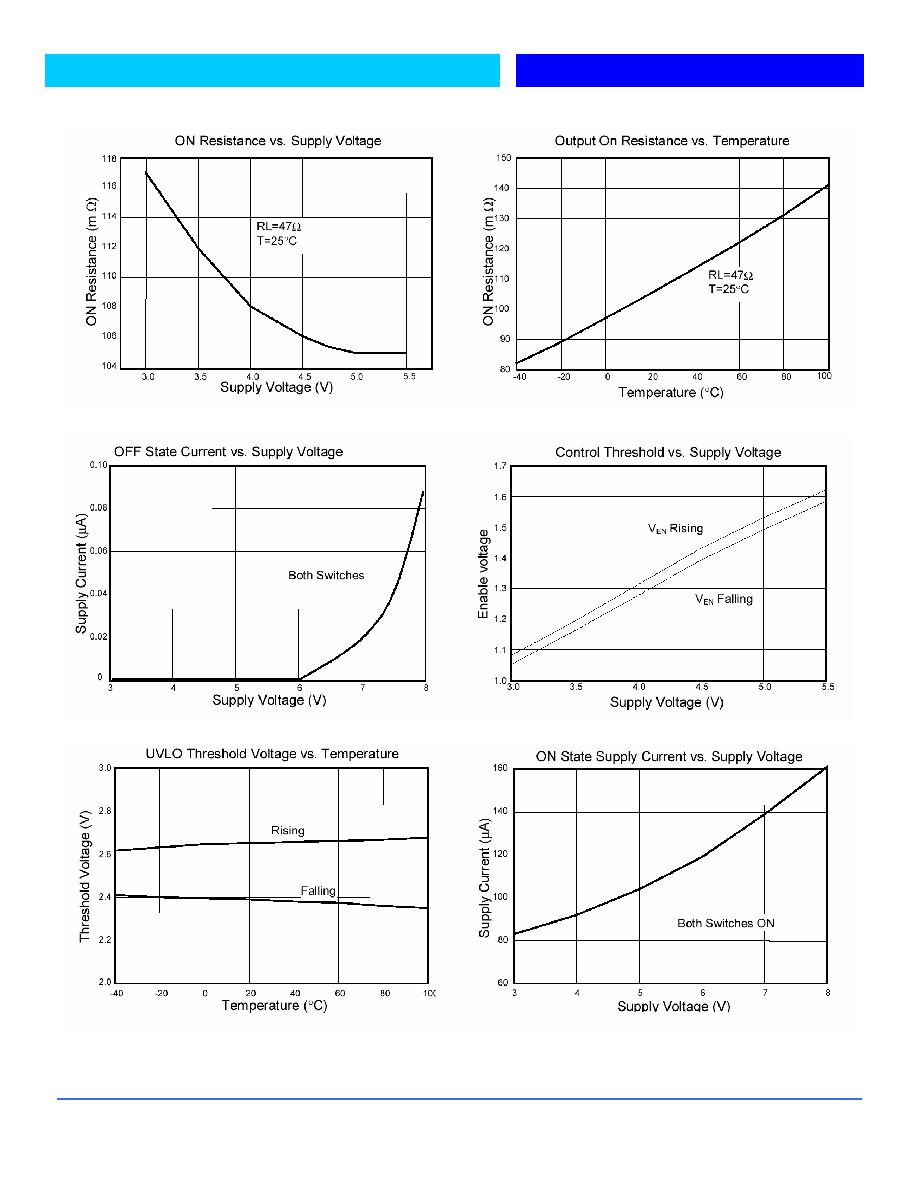
Power Switch
The power switch is an N-Channel MOSFET with a maximum on-state resistance of 140m
(V
IN
= 5V). the power switch supplies a
minimum of 500mA per switch.
Enable
The Logic enable disables the power switch and the bias for the charge pump, driver and other circuitry to reduce the supply current to
less than 5
�
A when a logic high is present on the EN pin for B2526-2 or a logic low is present on EN for B2526-1. The enable input
is compatible with both TTL and CMOS logic levels.
Driver
The driver controls the gate voltage of the power switch. To Limit large current surges the driver incorporates circuitry that controls
the rise and fall times of the output voltage.
Charge Pump
An internal charge pump supplies power to the driver circuit and provides the necessary voltages to pull the gate of the MOSFET
above the source.
Fault Flag FLG (A)/(B)
FLG is a N-Channel, open drain MOSFET output. The fault flag is active (low) for one or more of the following conditions: under-
voltage (while 2V
<
V
IN
<
2.7V), current limit or thermal shutdown. The flag output MOSFET is capable of sinking a 10mA load to
typically 100mV above ground. Multiple FLG pins may be "wired NORed" to a common pull-up resistor.
Thermal Shutdown
An internal thermal sense circuit shuts off the power switch when the junction temperature rises to approximately 150
�
C. Hysteresis is
built into the thermal sense circuit.
Current Sense
A sense FET monitors the current supplied to the load. When an overload or short circuit is encountered, the current sense circuitry
sends a control signal to the driver. The driver in turn reduces the gate voltage and sends the power FET into its saturation region,
which switches the output into a constant current mode. The 2526 current-limit profile exhibits a small foldback effect of
approximately 500mA. Once this current-limit threshold is exceeded the device enters constant current mode. The constant current is
specified as the short circuit current limit in the "Electrical Characteristics" table. It is important to note that the 2526 will deliver load
current up to the current-limit Threshold which is typically 1.6A (2.2Amax)."
Under-Voltage Lockout (UVLO)
UVLO prevents the output MOSFET form turning on until V
IN
exceeds 2.5V. In the under-voltage state, the FLG will be low. After
the switch turns on, if the voltage drops below approximately 2.3V, UVLO shuts off the output MOSFET and signals fault flag.
Under-voltage detection functions only when at least one switch is enabled.
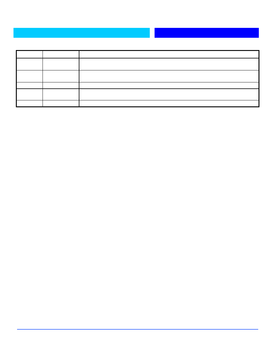
PIN DESCRIPTION
Pin No.
Pin Name
Pin Function
1 & 4
EN (A)/(B)
Enable (Input): Logic-compatible enables input. High input > 2.1V typical.
Low input < 1.9V typical (B2526-1 active high, B2526 -2 active low).
2 & 3
FLAG (A)/(B)
Fault Flag (Output): Active-low, open-drain output. Indicates over current,
UVLO and thermal shutdown.
6
GND
Ground: Supply return.
7 V
IN
Supply Input: Output MOSFET drain. Also supplies IC's internal circuitry. Connect to positive
supply.
8 & 5
V
OUT
(A)/(B)
Switch Output: Output MOSFET source. Typically connect to switched side of load.
Bay Linear, Inc
2418Armstrong St., Livermore CA USA 94550 Tel: (925) 606-5950, Fax: (925) 940-9556 www.baylinear.com
B2526
Bay Linear, Inc
2418Armstrong St., Livermore CA USA 94550 Tel: (925) 606-5950, Fax: (925) 940-9556 www.baylinear.com
B2526
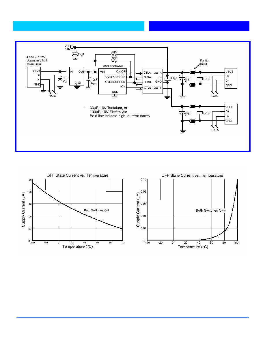
Two-Port Self Powered Hub (Using B2526 & B4300)
B2526
B4300