 | –≠–ª–µ–∫—Ç—Ä–æ–Ω–Ω—ã–π –∫–æ–º–ø–æ–Ω–µ–Ω—Ç: BT869KRF | –°–∫–∞—á–∞—Ç—å:  PDF PDF  ZIP ZIP |
Document Outline
- Bt868/Bt869
- Functional Block Diagram
- Distinguishing Features
- Applications
- Table of Contents
- List of Figures
- List of Tables
- 1.0 Functional Description
- 1.1 Pin Descriptions
- 1.2 GUI Controller Programmability and Frequency Requirement
- 1.3 Circuit Description
- 1.3.1 Overview
- 1.3.2 Reset
- 1.3.3 Timing Registers
- 1.3.4 Device Initialization
- 1.3.5 Auto Configuration
- 1.3.6 Clocking and Timing Generation
- 1.3.7 Master and Slave Modes
- 1.3.8 Input Formats
- 1.3.9 Pixel Input Timing
- 1.3.10 Output Modes
- 1.3.11 YCrCb Inputs
- 1.3.12 RGB Inputs
- 1.3.13 Video Amplitude Scaling
- 1.3.14 Input Pixel Horizontal Sync
- 1.3.15 Input Pixel Vertical Sync
- 1.3.16 Input Pixel Blanking
- 1.3.17 Overscan Compensation and Flicker Filtering
- 1.3.18 VGA Compatibility
- 1.3.19 Analog Horizontal Sync
- 1.3.20 Analog Vertical Sync
- 1.3.21 Analog Video Blanking
- 1.3.22 Video Standards
- Figure 1�5. Interlaced 525-Line (NTSC) Video Timing
- Figure 1�6. Interlaced 525-Line (PAL-M) Video Timing
- Figure 1�7. Interlaced 625-Line (PALÖB, D, G, H, I, Nc) Video Timing (Fields 1Ö4)
- Figure 1�8. Interlaced 625-Line (PALÖB, D, G, H, I, Nc) Video Timing (Fields 5Ö8)
- Figure 1�9. Interlaced 625-Line (PALÖN) Video Timing (Fields 1Ö4)
- Figure 1�10. Interlaced 625-Line (PALÖN) Video Timing (Fields 5Ö8)
- Figure 1�11. Noninterlaced 262-Line (NTSC) Video Timing
- Figure 1�12. Noninterlaced 262-Line (PALÖM) Video Timing
- Figure 1�13. Noninterlaced 312-Line (PALÖB, D, G, H, I, N, Nc) Video Timing
- 1.3.23 Subcarrier Generation
- 1.3.24 Burst Generation
- 1.3.25 Chrominance Disable
- 1.3.26 Digital Processing
- 1.3.27 Subcarrier Phasing
- 1.3.28 Noninterlaced Operation
- 1.3.29 Closed Captioning
- 1.3.30 Internal Color Bars
- 1.3.31 Macrovision Encoding
- 1.3.32 Outputs
- 1.3.33 Output Connection Status
- 1.3.34 Output Filtering and SINX/X Compensation
- 1.3.35 Power-Down Modes
- 1.3.36 Serial Interface
- 2.0 Internal Registers
- 3.0 PC Board Considerations
- 4.0 Parametric Information
- Appendix A . Scaling and I/O Timing Register Calculations
- Table A-1. Video Formats
- Table A-2. Constant Values Dependent on Encoding Mode
- Figure A-1. Overscan Compensation, 640x480 NTSC, 20 Clock Hblank
- Figure A-2. Overscan Compensation, 640x480 PAL, 20 Clock Hblank
- Figure A-3. Overscan Compensation, 800x600 NTSC
- Figure A-4. Overscan Compensation, 800x600 PAL
- Table A-3. Overscan Values, 640x480 NTSC, 1 Pixel Resolution, 2.5 ms Hblank� (1 of 3)
- Table A-4. Overscan Values, 640x480 NTSC, 8 Pixel Resolution, 2.5 ms Hblank�
- Table A-5. Overscan Values, 640x480 NTSC, 9 Pixel Resolution, 2.5 ms Hblank�
- Table A-6. Overscan Values, 640x480 PAL, 1 Pixel Resolution, 2.5 ms Hblank� (1 of 4)
- Table A-7. Overscan Values, 640x480 PAL, 8 Pixel Resolution, 2.5 ms Hblank (1 of 2)
- Table A-8. Overscan Values, 640x480 PAL, 9 Pixel Resolution, 2.5 ms Hblank�
- Table A-9. Overscan Values, 800x600 NTSC� (1 of 5)
- Table A-10. Overscan Values, 800x600, PAL, > 2.5 ms Hblank� (1 of 3)
- Appendix B . Approved Crystal Vendors
- Sales Offices

Data Sheet
100123B
September 2000
Bt868/Bt869
Flicker-Free Video Encoder with Ultrascale
TM
Technology
The Bt868/869 is specifically designed for video systems requiring the generation of
high-quality flicker-free composite and Y/C (S-video) signals from various YCrCb or
RGB digital streams. The Bt868/869 accepts any input format from 640 x 480 to
800 x 600 resolution.
The Bt868/869 uses Conexant's UltraScaleTM technology to provide the most
advanced vertical and horizontal scaling necessary for the display of non-interlaced
data on interlaced devices such as the TV. The UltraScaleTM technology converts the
lines of input pixel data to the appropriate number of output lines for producing a
full-screen, high-quality image.
The Bt868/869 performs 5-line vertical filtering, which includes poly phase
interpolation scaling for overscan compensation and flicker filtering. Horizontal
scaling for overscan compensation is achieved by altering the encoder clock
frequency. This approach preserves all of the high frequency components of the
input signals, which are essential for the highest quality display of text intensive
images such as web pages on TVs. The amount of flicker filtering and overscan
compensation is programmable.
Worldwide video standards are supported, including NTSC-M (N. America,
Taiwan, Japan), PAL-B,D,G,H,I (Europe, Asia), PAL-M (Brazil), PAL-N (Uruguay,
Paraguay), and PAL-Nc (Argentina). Bt868 and Bt869 are functionally identical, with
the exception that Bt869 can output Macrovision Level 7.0 anticopy algorithm.
Functional Block Diagram
Input
Flicker
FIFO
Video
XTAL
PLL
DAC
DACA
DACB
Internal
COMP
FSADJUST
VREF
BIAS
VBIAS
P[23:0]
XTALIN
XTALOUT
CLKO
CLKI
SIC
SID
ALTADDR
HSYNC*
VSYNC*
BLANK*
FIELD
RESET*
SLEEP
SLAVE
PAL
MUX
Encoder
Color Space
DACC
Timing
Serial
Clock
DEMUX
Interface
Filter/Scaler
Conversion
Reference
Generation
OSC
GEN
Distinguishing Features
∑
Digital RGB or YCrCb non-interlaced
input to interlaced or non-interlaced
analog TV output modes:
YCrCb Modes:
≠ 16-bit 4:2:2 multiplexed 8-bit
≠ 24-bit 4:4:4 multiplexed 12-bit
≠ 24-bit 4:4:4 non-multiplexed 24-bit
RGB Modes:
≠ 15/16 bit 5:6:5 RGB multiplexed 8-bit
≠ 24-bit 8:8:8 RGB mulitplexed 12-bit
≠ 24-bit 8:8:8 RGB non-multiplexed
24-bit
∑
Digital RGB non-interlaced input to
analog RGB noninterlaced (VGA/SVGA)
output modes:
≠ 15/16 bit 5:6:5 RGB multiplexed 8-bit
≠ 24-bit 8:8:8 RGB mulitplexed 12-bit
≠ 24-bit 8:8:8 RGB non-multiplexed
24-bit
∑
Support for NTSC/PAL outputs in the
following modes:
≠ Interlaced and non-interlaced outputs
≠ S-video output (simultaneous with
composite NTSC or PAL outputs)
≠ Component YUV analog output mode
∑
5-line vertical filtering scaling for
overscan compensation and flicker
filtering
∑
CCIR601 compatible input mode
∑
Luma and chroma comb filtering
∑
3 x 10-bit DACs
∑
6 MHz Luma bandwidth
∑
Macrovision 7.0 copy protection
∑
80-pin PQFP package
∑
3.3 V operation with 5 V tolerant IOs
∑
2-line serial programming interface
∑
Power-Down modes
∑
Master/slave video timing operation
∑
TV connected register flag
∑
Automatic configuration
Applications
∑
Desktop/Portable PCs with TV-Out
∑
Living-room PCs
∑
Internet PC/TVs
∑
Internet Appliances

100123B
Conexant
© 2000,
Conexant Systems, Inc.
All Rights Reserved.
Information in this document is provided in connection with Conexant Systems, Inc. ("Conexant") products. These materials are
provided by Conexant as a service to its customers and may be used for informational purposes only. Conexant assumes no
responsibility for errors or omissions in these materials. Conexant may make changes to specifications and product descriptions at
any time, without notice. Conexant makes no commitment to update the information and shall have no responsibility whatsoever for
conflicts or incompatibilities arising from future changes to its specifications and product descriptions.
No license, express or implied, by estoppel or otherwise, to any intellectual property rights is granted by this document. Except as
provided in Conexant's Terms and Conditions of Sale for such products, Conexant assumes no liability whatsoever.
THESE MATERIALS ARE PROVIDED "AS IS" WITHOUT WARRANTY OF ANY KIND, EITHER EXPRESS OR IMPLIED, RELATING
TO SALE AND/OR USE OF CONEXANT PRODUCTS INCLUDING LIABILITY OR WARRANTIES RELATING TO FITNESS FOR A
PARTICULAR PURPOSE, CONSEQUENTIAL OR INCIDENTAL DAMAGES, MERCHANTABILITY, OR INFRINGEMENT OF ANY
PATENT, COPYRIGHT OR OTHER INTELLECTUAL PROPERTY RIGHT. CONEXANT FURTHER DOES NOT WARRANT THE
ACCURACY OR COMPLETENESS OF THE INFORMATION, TEXT, GRAPHICS OR OTHER ITEMS CONTAINED WITHIN THESE
MATERIALS. CONEXANT SHALL NOT BE LIABLE FOR ANY SPECIAL, INDIRECT, INCIDENTAL, OR CONSEQUENTIAL
DAMAGES, INCLUDING WITHOUT LIMITATION, LOST REVENUES OR LOST PROFITS, WHICH MAY RESULT FROM THE USE
OF THESE MATERIALS.
Conexant products are not intended for use in medical, lifesaving or life sustaining applications. Conexant customers using or selling
Conexant products for use in such applications do so at their own risk and agree to fully indemnify Conexant for any damages
resulting from such improper use or sale.
The following are trademarks of Conexant Systems, Inc.: ConexantTM, the Conexant C symbol, and "What's Next in Communications
Technologies"TM. Product names or services listed in this publication are for identification purposes only, and may be trademarks of
third parties. Third-party brands and names are the property of their respective owners.
For additional disclaimer information, please consult Conexant's Legal Information posted at
www.conexant.com
, which is
incorporated by reference.
Reader Response: Conexant strives to produce quality documentation and welcomes your feedback. Please send comments and
suggestions to
tech.pubs@conexant.com
. For technical questions, contact your local Conexant
sales office
or field applications
engineer.
Ordering Information
Model Number
Package
Ambient Temperature Range
Reduced Features
Bt868KRF
80-pin PQFP
0
∞
C to +70
∞
C
No Macrovision Feature
Bt869KRF
80-pin PQFP
0
∞
C to +70
∞
C
--

100123B
Conexant
iii
Table of Contents
List of Figures
. . . . . . . . . . . . . . . . . . . . . . . . . . . . . . . . . . . . . . . . . . . . . . . . . . . . . . . . . . . . . . . . . . . . . . . . vii
List of Tables
. . . . . . . . . . . . . . . . . . . . . . . . . . . . . . . . . . . . . . . . . . . . . . . . . . . . . . . . . . . . . . . . . . . . . . . . . . ix
1.0
Functional Description
. . . . . . . . . . . . . . . . . . . . . . . . . . . . . . . . . . . . . . . . . . . . . . . . . . . . . . . . . . 1-1
1.1
Pin Descriptions
. . . . . . . . . . . . . . . . . . . . . . . . . . . . . . . . . . . . . . . . . . . . . . . . . . . . . . . . . . . . 1-1
1.2
GUI Controller Programmability and Frequency Requirement
. . . . . . . . . . . . . . . . . . . . . . . . . . 1-6
1.3
Circuit Description
. . . . . . . . . . . . . . . . . . . . . . . . . . . . . . . . . . . . . . . . . . . . . . . . . . . . . . . . . . 1-9
1.3.1
Overview
. . . . . . . . . . . . . . . . . . . . . . . . . . . . . . . . . . . . . . . . . . . . . . . . . . . . . . . . . . . . 1-9
1.3.2
Reset
. . . . . . . . . . . . . . . . . . . . . . . . . . . . . . . . . . . . . . . . . . . . . . . . . . . . . . . . . . . . . . . 1-9
1.3.3
Timing Registers
. . . . . . . . . . . . . . . . . . . . . . . . . . . . . . . . . . . . . . . . . . . . . . . . . . . . . . 1-9
1.3.4
Device Initialization
. . . . . . . . . . . . . . . . . . . . . . . . . . . . . . . . . . . . . . . . . . . . . . . . . . . 1-10
1.3.5
Auto Configuration
. . . . . . . . . . . . . . . . . . . . . . . . . . . . . . . . . . . . . . . . . . . . . . . . . . . . 1-10
1.3.6
Clocking and Timing Generation
. . . . . . . . . . . . . . . . . . . . . . . . . . . . . . . . . . . . . . . . . . 1-13
1.3.7
Master and Slave Modes
. . . . . . . . . . . . . . . . . . . . . . . . . . . . . . . . . . . . . . . . . . . . . . . 1-14
1.3.8
Input Formats
. . . . . . . . . . . . . . . . . . . . . . . . . . . . . . . . . . . . . . . . . . . . . . . . . . . . . . . 1-15
1.3.9
Pixel Input Timing
. . . . . . . . . . . . . . . . . . . . . . . . . . . . . . . . . . . . . . . . . . . . . . . . . . . . 1-15
1.3.10
Output Modes
. . . . . . . . . . . . . . . . . . . . . . . . . . . . . . . . . . . . . . . . . . . . . . . . . . . . . . . 1-15
1.3.11
YCrCb Inputs
. . . . . . . . . . . . . . . . . . . . . . . . . . . . . . . . . . . . . . . . . . . . . . . . . . . . . . . . 1-16
1.3.12
RGB Inputs
. . . . . . . . . . . . . . . . . . . . . . . . . . . . . . . . . . . . . . . . . . . . . . . . . . . . . . . . . 1-17
1.3.13
Video Amplitude Scaling
. . . . . . . . . . . . . . . . . . . . . . . . . . . . . . . . . . . . . . . . . . . . . . . . 1-17
1.3.14
Input Pixel Horizontal Sync
. . . . . . . . . . . . . . . . . . . . . . . . . . . . . . . . . . . . . . . . . . . . . . 1-18
1.3.15
Input Pixel Vertical Sync
. . . . . . . . . . . . . . . . . . . . . . . . . . . . . . . . . . . . . . . . . . . . . . . . 1-19
1.3.16
Input Pixel Blanking
. . . . . . . . . . . . . . . . . . . . . . . . . . . . . . . . . . . . . . . . . . . . . . . . . . . 1-19
1.3.17
Overscan Compensation and Flicker Filtering
. . . . . . . . . . . . . . . . . . . . . . . . . . . . . . . . . 1-20
1.3.18
VGA Compatibility
. . . . . . . . . . . . . . . . . . . . . . . . . . . . . . . . . . . . . . . . . . . . . . . . . . . . 1-21
1.3.19
Analog Horizontal Sync
. . . . . . . . . . . . . . . . . . . . . . . . . . . . . . . . . . . . . . . . . . . . . . . . 1-21
1.3.20
Analog Vertical Sync
. . . . . . . . . . . . . . . . . . . . . . . . . . . . . . . . . . . . . . . . . . . . . . . . . . . 1-21
1.3.21
Analog Video Blanking
. . . . . . . . . . . . . . . . . . . . . . . . . . . . . . . . . . . . . . . . . . . . . . . . . 1-21
1.3.22
Video Standards
. . . . . . . . . . . . . . . . . . . . . . . . . . . . . . . . . . . . . . . . . . . . . . . . . . . . . . 1-21
1.3.23
Subcarrier Generation
. . . . . . . . . . . . . . . . . . . . . . . . . . . . . . . . . . . . . . . . . . . . . . . . . 1-29
1.3.24
Burst Generation
. . . . . . . . . . . . . . . . . . . . . . . . . . . . . . . . . . . . . . . . . . . . . . . . . . . . . 1-30
1.3.25
Chrominance Disable
. . . . . . . . . . . . . . . . . . . . . . . . . . . . . . . . . . . . . . . . . . . . . . . . . . 1-30
1.3.26
Digital Processing
. . . . . . . . . . . . . . . . . . . . . . . . . . . . . . . . . . . . . . . . . . . . . . . . . . . . 1-30
1.3.27
Subcarrier Phasing
. . . . . . . . . . . . . . . . . . . . . . . . . . . . . . . . . . . . . . . . . . . . . . . . . . . . 1-31

Table of Contents
Bt868/Bt869
Flicker-Free Video Encoder with Ultrascale
TM
Technology
iv
Conexant
100123B
1.3.28
Noninterlaced Operation
. . . . . . . . . . . . . . . . . . . . . . . . . . . . . . . . . . . . . . . . . . . . . . . . 1-31
1.3.29
Closed Captioning
. . . . . . . . . . . . . . . . . . . . . . . . . . . . . . . . . . . . . . . . . . . . . . . . . . . . 1-32
1.3.30
Internal Color Bars
. . . . . . . . . . . . . . . . . . . . . . . . . . . . . . . . . . . . . . . . . . . . . . . . . . . . 1-32
1.3.31
Macrovision Encoding
. . . . . . . . . . . . . . . . . . . . . . . . . . . . . . . . . . . . . . . . . . . . . . . . . 1-32
1.3.32
Outputs
. . . . . . . . . . . . . . . . . . . . . . . . . . . . . . . . . . . . . . . . . . . . . . . . . . . . . . . . . . . . 1-33
1.3.33
Output Connection Status
. . . . . . . . . . . . . . . . . . . . . . . . . . . . . . . . . . . . . . . . . . . . . . . 1-33
1.3.34
Output Filtering and SINX/X Compensation
. . . . . . . . . . . . . . . . . . . . . . . . . . . . . . . . . . 1-33
1.3.35
Power-Down Modes
. . . . . . . . . . . . . . . . . . . . . . . . . . . . . . . . . . . . . . . . . . . . . . . . . . . 1-34
1.3.36
Serial Interface
. . . . . . . . . . . . . . . . . . . . . . . . . . . . . . . . . . . . . . . . . . . . . . . . . . . . . . . 1-34
2.0
Internal Registers
. . . . . . . . . . . . . . . . . . . . . . . . . . . . . . . . . . . . . . . . . . . . . . . . . . . . . . . . . . . . . . 2-1
2.1
Essential Registers
. . . . . . . . . . . . . . . . . . . . . . . . . . . . . . . . . . . . . . . . . . . . . . . . . . . . . . . . . . . 2-3
2.2
Writing Addresses
. . . . . . . . . . . . . . . . . . . . . . . . . . . . . . . . . . . . . . . . . . . . . . . . . . . . . . . . . . . . 2-3
2.3
Reading Information
. . . . . . . . . . . . . . . . . . . . . . . . . . . . . . . . . . . . . . . . . . . . . . . . . . . . . . . . . . 2-3
3.0
PC Board Considerations
. . . . . . . . . . . . . . . . . . . . . . . . . . . . . . . . . . . . . . . . . . . . . . . . . . . . . . . . 3-1
3.1
Component Placement
. . . . . . . . . . . . . . . . . . . . . . . . . . . . . . . . . . . . . . . . . . . . . . . . . . . . . . . 3-1
3.2
Power and Ground Planes
. . . . . . . . . . . . . . . . . . . . . . . . . . . . . . . . . . . . . . . . . . . . . . . . . . . . . 3-1
3.3
Decoupling
. . . . . . . . . . . . . . . . . . . . . . . . . . . . . . . . . . . . . . . . . . . . . . . . . . . . . . . . . . . . . . . . 3-5
3.3.1
Device Decoupling
. . . . . . . . . . . . . . . . . . . . . . . . . . . . . . . . . . . . . . . . . . . . . . . . . . . . . 3-5
3.3.2
Power Supply Decoupling
. . . . . . . . . . . . . . . . . . . . . . . . . . . . . . . . . . . . . . . . . . . . . . . . 3-5
3.3.3
COMP Decoupling
. . . . . . . . . . . . . . . . . . . . . . . . . . . . . . . . . . . . . . . . . . . . . . . . . . . . . 3-5
3.3.4
VREF Decoupling
. . . . . . . . . . . . . . . . . . . . . . . . . . . . . . . . . . . . . . . . . . . . . . . . . . . . . . 3-5
3.3.5
VBIAS Decoupling
. . . . . . . . . . . . . . . . . . . . . . . . . . . . . . . . . . . . . . . . . . . . . . . . . . . . . 3-5
3.4
Signal Interconnect
. . . . . . . . . . . . . . . . . . . . . . . . . . . . . . . . . . . . . . . . . . . . . . . . . . . . . . . . . . 3-6
3.4.1
Digital Signal Interconnect
. . . . . . . . . . . . . . . . . . . . . . . . . . . . . . . . . . . . . . . . . . . . . . . 3-6
3.4.2
Analog Signal Interconnect
. . . . . . . . . . . . . . . . . . . . . . . . . . . . . . . . . . . . . . . . . . . . . . . 3-6
3.5
Applications Information
. . . . . . . . . . . . . . . . . . . . . . . . . . . . . . . . . . . . . . . . . . . . . . . . . . . . . . 3-7
3.5.1
Electrostatic Discharge and Latchup Considerations
. . . . . . . . . . . . . . . . . . . . . . . . . . . . 3-7
3.5.2
Clock and Subcarrier Stability
. . . . . . . . . . . . . . . . . . . . . . . . . . . . . . . . . . . . . . . . . . . . . 3-7
3.5.3
Filtering Radio Frequency Modulator Connection
. . . . . . . . . . . . . . . . . . . . . . . . . . . . . . . 3-8
3.6
Bt868/Bt869 Evaluation Board
. . . . . . . . . . . . . . . . . . . . . . . . . . . . . . . . . . . . . . . . . . . . . . . . . . 3-9
3.7
Serial Interface
. . . . . . . . . . . . . . . . . . . . . . . . . . . . . . . . . . . . . . . . . . . . . . . . . . . . . . . . . . . . 3-16
3.7.1
Data Transfer on the Serial Interface Bus
. . . . . . . . . . . . . . . . . . . . . . . . . . . . . . . . . . . . 3-16
4.0
Parametric Information
. . . . . . . . . . . . . . . . . . . . . . . . . . . . . . . . . . . . . . . . . . . . . . . . . . . . . . . . . 4-1
4.1
DC Electrical Parameters
. . . . . . . . . . . . . . . . . . . . . . . . . . . . . . . . . . . . . . . . . . . . . . . . . . . . . 4-1
4.2
AC Electrical Parameters
. . . . . . . . . . . . . . . . . . . . . . . . . . . . . . . . . . . . . . . . . . . . . . . . . . . . . 4-4
4.3
Mechanical Drawing
. . . . . . . . . . . . . . . . . . . . . . . . . . . . . . . . . . . . . . . . . . . . . . . . . . . . . . . . . 4-9
Appendix A. Scaling and I/O Timing Register Calculations
. . . . . . . . . . . . . . . . . . . . . . . . . . . . . . . A-1
Appendix B. Approved Crystal Vendors
. . . . . . . . . . . . . . . . . . . . . . . . . . . . . . . . . . . . . . . . . . . . . . . . . B-1

Bt868/Bt869
List of Figures
Flicker-Free Video Encoder with Ultrascale
TM
Technology
100123B
Conexant
vii
List of Figures
Figure 1-1.
Pinout Diagram . . . . . . . . . . . . . . . . . . . . . . . . . . . . . . . . . . . . . . . . . . . . . . . . . . . . . . . . . . 1-1
Figure 1-2.
Flicker Filter Control Diagram--External Use . . . . . . . . . . . . . . . . . . . . . . . . . . . . . . . . . . . 1-7
Figure 1-3.
Encoder Core. . . . . . . . . . . . . . . . . . . . . . . . . . . . . . . . . . . . . . . . . . . . . . . . . . . . . . . . . . . . 1-8
Figure 1-4.
Decimation Filter at Fs=27 MHz. . . . . . . . . . . . . . . . . . . . . . . . . . . . . . . . . . . . . . . . . . . . . 1-16
Figure 1-5.
Interlaced 525-Line (NTSC) Video Timing . . . . . . . . . . . . . . . . . . . . . . . . . . . . . . . . . . . . . 1-22
Figure 1-6.
Interlaced 525-Line (PAL-M) Video Timing . . . . . . . . . . . . . . . . . . . . . . . . . . . . . . . . . . . . 1-23
Figure 1-7.
Interlaced 625-Line (PAL≠B, D, G, H, I, Nc) Video Timing (Fields 1≠4) . . . . . . . . . . . . . . . 1-24
Figure 1-8.
Interlaced 625-Line (PAL≠B, D, G, H, I, Nc) Video Timing (Fields 5≠8) . . . . . . . . . . . . . . . 1-25
Figure 1-9.
Interlaced 625-Line (PAL≠N) Video Timing (Fields 1≠4) . . . . . . . . . . . . . . . . . . . . . . . . . . 1-26
Figure 1-10.
Interlaced 625-Line (PAL≠N) Video Timing (Fields 5≠8) . . . . . . . . . . . . . . . . . . . . . . . . . . 1-27
Figure 1-11.
Noninterlaced 262-Line (NTSC) Video Timing . . . . . . . . . . . . . . . . . . . . . . . . . . . . . . . . . . 1-28
Figure 1-12.
Noninterlaced 262-Line (PAL≠M) Video Timing . . . . . . . . . . . . . . . . . . . . . . . . . . . . . . . . 1-28
Figure 1-13.
Noninterlaced 312-Line (PAL≠B, D, G, H, I, N, Nc) Video Timing . . . . . . . . . . . . . . . . . . . 1-29
Figure 1-14.
Three-Stage Chroma Filter. . . . . . . . . . . . . . . . . . . . . . . . . . . . . . . . . . . . . . . . . . . . . . . . . 1-30
Figure 1-15.
Luminance Upsampling Filter Response . . . . . . . . . . . . . . . . . . . . . . . . . . . . . . . . . . . . . . 1-31
Figure 3-1.
Power Plane Illustration . . . . . . . . . . . . . . . . . . . . . . . . . . . . . . . . . . . . . . . . . . . . . . . . . . . 3-2
Figure 3-2.
Connection Diagram for Output Filters and Other Key Passive Components . . . . . . . . . . . . 3-3
Figure 3-3.
Complete Bt868/Bt869 Recommended Layout . . . . . . . . . . . . . . . . . . . . . . . . . . . . . . . . . . 3-4
Figure 3-4.
Bt868/Bt869 Evaluation Board. . . . . . . . . . . . . . . . . . . . . . . . . . . . . . . . . . . . . . . . . . . . . . 3-10
Figure 3-5.
SID/SIC Diagram . . . . . . . . . . . . . . . . . . . . . . . . . . . . . . . . . . . . . . . . . . . . . . . . . . . . . . . . 3-16
Figure 4-1.
Interface Timing . . . . . . . . . . . . . . . . . . . . . . . . . . . . . . . . . . . . . . . . . . . . . . . . . . . . . . . . . 4-6
Figure 4-2.
Master Mode with Flicker Filter Interface Timing. . . . . . . . . . . . . . . . . . . . . . . . . . . . . . . . . 4-7
Figure 4-3.
Slave Mode with Flicker Filter Interface Timing . . . . . . . . . . . . . . . . . . . . . . . . . . . . . . . . . . 4-8
Figure A-1.
Overscan Compensation, 640x480 NTSC, 20 Clock Hblank . . . . . . . . . . . . . . . . . . . . . . . . A-2
Figure A-2.
Overscan Compensation, 640x480 PAL, 20 Clock Hblank . . . . . . . . . . . . . . . . . . . . . . . . . A-3
Figure A-3.
Overscan Compensation, 800x600 NTSC . . . . . . . . . . . . . . . . . . . . . . . . . . . . . . . . . . . . . . A-4
Figure A-4.
Overscan Compensation, 800x600 PAL . . . . . . . . . . . . . . . . . . . . . . . . . . . . . . . . . . . . . . . A-5

List of Figures
Bt868/Bt869
Flicker-Free Video Encoder with Ultrascale
TM
Technology
viii
Conexant
100123B

Bt868/Bt869
List of Tables
Flicker-Free Video Encoder with Ultrascale
TM
Technology
100123B
Conexant
ix
List of Tables
Table 1-1.
Pin Assignments . . . . . . . . . . . . . . . . . . . . . . . . . . . . . . . . . . . . . . . . . . . . . . . . . . . . . . . . . . 1-2
Table 1-2.
Data Pin Assignments for Multiplexed Modes. . . . . . . . . . . . . . . . . . . . . . . . . . . . . . . . . . . . 1-5
Table 1-3.
Data Pin Assignments for Non-multiplexed Modes . . . . . . . . . . . . . . . . . . . . . . . . . . . . . . . . 1-5
Table 1-4.
Programmability and Frequency Requirement . . . . . . . . . . . . . . . . . . . . . . . . . . . . . . . . . . . 1-6
Table 1-5.
Auto-Configuration Modes 0≠3--RGB Input. . . . . . . . . . . . . . . . . . . . . . . . . . . . . . . . . . . . 1-11
Table 1-6.
Auto-Configuration Modes 4≠7--YCrCb Input . . . . . . . . . . . . . . . . . . . . . . . . . . . . . . . . . . 1-12
Table 1-7.
Video Modes . . . . . . . . . . . . . . . . . . . . . . . . . . . . . . . . . . . . . . . . . . . . . . . . . . . . . . . . . . . . 1-17
Table 1-8.
Video Levels . . . . . . . . . . . . . . . . . . . . . . . . . . . . . . . . . . . . . . . . . . . . . . . . . . . . . . . . . . . . 1-18
Table 2-1.
Register Bit Map . . . . . . . . . . . . . . . . . . . . . . . . . . . . . . . . . . . . . . . . . . . . . . . . . . . . . . . . . . 2-1
Table 2-2.
Read-Back Bit Map . . . . . . . . . . . . . . . . . . . . . . . . . . . . . . . . . . . . . . . . . . . . . . . . . . . . . . . . 2-4
Table 2-3.
Data Details Defined . . . . . . . . . . . . . . . . . . . . . . . . . . . . . . . . . . . . . . . . . . . . . . . . . . . . . . . 2-4
Table 2-4.
Programming Detail . . . . . . . . . . . . . . . . . . . . . . . . . . . . . . . . . . . . . . . . . . . . . . . . . . . . . . . 2-4
Table 3-1.
Typical Parts List for Key Passive Components. . . . . . . . . . . . . . . . . . . . . . . . . . . . . . . . . . . 3-3
Table 4-1.
Recommended Operating Conditions . . . . . . . . . . . . . . . . . . . . . . . . . . . . . . . . . . . . . . . . . . 4-1
Table 4-2.
Absolute Maximum Rating . . . . . . . . . . . . . . . . . . . . . . . . . . . . . . . . . . . . . . . . . . . . . . . . . . 4-1
Table 4-3.
DC Characteristics. . . . . . . . . . . . . . . . . . . . . . . . . . . . . . . . . . . . . . . . . . . . . . . . . . . . . . . . . 4-2
Table 4-4.
AC Characteristics . . . . . . . . . . . . . . . . . . . . . . . . . . . . . . . . . . . . . . . . . . . . . . . . . . . . . . . . . 4-4
Table A-1.
Video Formats . . . . . . . . . . . . . . . . . . . . . . . . . . . . . . . . . . . . . . . . . . . . . . . . . . . . . . . . . . . . A-1
Table A-2.
Constant Values Dependent on Encoding Mode . . . . . . . . . . . . . . . . . . . . . . . . . . . . . . . . . . A-2
Table A-3.
Overscan Values, 640x480 NTSC, 1 Pixel Resolution, 2.5 ms Hblank . . . . . . . . . . . . . . . . . A-5
Table A-4.
Overscan Values, 640x480 NTSC, 8 Pixel Resolution, 2.5 ms Hblank . . . . . . . . . . . . . . . . . A-7
Table A-5.
Overscan Values, 640x480 NTSC, 9 Pixel Resolution, 2.5 ms Hblank . . . . . . . . . . . . . . . . . A-8
Table A-6.
Overscan Values, 640x480 PAL, 1 Pixel Resolution, 2.5 ms Hblank. . . . . . . . . . . . . . . . . . . A-8
Table A-7.
Overscan Values, 640x480 PAL, 8 Pixel Resolution, 2.5 ms Hblank. . . . . . . . . . . . . . . . . . A-11
Table A-8.
Overscan Values, 640x480 PAL, 9 Pixel Resolution, 2.5 ms Hblank. . . . . . . . . . . . . . . . . . A-12
Table A-9.
Overscan Values, 800x600 NTSC . . . . . . . . . . . . . . . . . . . . . . . . . . . . . . . . . . . . . . . . . . . . A-13
Table A-10.
Overscan Values, 800x600, PAL, > 2.5 ms Hblank . . . . . . . . . . . . . . . . . . . . . . . . . . . . . . . A-17

List of Tables
Bt868/Bt869
Flicker-Free Video Encoder with Ultrascale
TM
Technology
x
Conexant
100123B

100123B
Conexant
1-1
1
1.0 Functional Description
1.1 Pin Descriptions
The pinout diagram is shown in
Figure 1-1
. Pin names, input/output assignments,
numbers and descriptions are listed in
Tables 1-2
and
1-3
.
Figure 1-1. Pinout Diagram
RESET
*
VDD
VDDM
AX
SI
C
P[0
]
P[1
]
P[2
]
P[3
]
P[4
]
P[5
]
P[6
]
P[7
]
SI
D
BLANK*
FIELD
VSYNC*
HSYNC*
VSS
P[23]
P[22]
P[21]
P[20]
P[19]
P[18]
SLEEP
AG
N
D
VDD_
I
80-pin PQFP
AGND
FSADJUST
VBIAS
VREF
COMP
VAA
AGND_DAC
DACA
VAA_DACA
DACB
VAA_DACB
DACC
VAA_DACC
CL
KI
VD
D_
CO
CL
K
O
VSS_
CO
VDD_
SO
VDD_X
XTALOUT
XTALIN
VSS_X
P[8
]
P[9
]
P[10
]
P[11
]
P[12
]
P[13
]
P[14]
P[15]
P[16]
P[17]
PA
L
SLA
V
E
AL
T
A
DDR
VSS
1
2
3
4
5
6
7
8
9
10
11
12
13
14
15
NC
NC
VSS
VDD
VSS_I
VSS_O
VDD_O
VDD
VSS_SI
VSS_
SO
16
17
18
19
20
41
42
43
44
45
46
47
48
49
50
51
52
53
54
55
56
57
58
59
60
40
39
38
37
36
35
34
33
32
31
30
29
28
27
26
25
24
23
22
21
61
62
63
64
65
66
67
68
69
70
71
72
73
74
75
76
77
78
79
80
V
AA_
PLL
A
G
ND_
PL
L
VDD_
SI
N/C
N/C
N/C
TEST

1.0 Functional Description
Bt868/Bt869
1.1 Pin Descriptions
Flicker-Free Video Encoder with Ultrascale
TM
Technology
1-2
Conexant
100123B
Table 1-1. Pin Assignments (1 of 3)
Pin Name
I/O
Pin #
Description
XTALIN
I
63
A crystal can be connected to these pins. The pixel clock output (CLKO) is
derived from these pins with a PLL. XTALIN can be driven as a CMOS input
pin.
XTALOUT
O
62
VDD_X
--
61
Crystal oscillator supply pin. This pin should be tied to the digital supply.
VSS_X
--
64
Crystal oscillator ground pin. This pin should be tied to the digital ground
plane.
VAA_PLL
--
59
Analog power for PLL. All VAA and VDD pins must be connected together on
the same PCB plane to prevent latchup.
AGND_PLL
--
58
Analog ground for PLL. All AGND and VSS pins must be connected together
on the same PCB plane to prevent latchup.
CLKO
O
56
Pixel clock output (TTL compatible). This pin is three-state if the CLKI pin
provides the encoder clock.
VDD_CO
--
57
Clock output supply pin. This pin should be tied to the digital supply.
VSS_CO
--
55
Clock output ground pin. This pin should be tied to the digital ground plane.
CLKI
I
54
Pixel clock input (TTL compatible). This may be used as either the encoder
clock or a delayed version of the CLKO pin synchronized with the pixel data
input.
RESET*
I
53
Reset control input (TTL compatible). A logical 0 resets and disables video
timing (horizontal, vertical, subcarrier counters to the start of VSYNC of first
field) and resets the serial interface registers). RESET* must be a logical 1
for normal operation.
SLEEP
I
52
Power-down control input (TTL compatible). A logical 1 configures the
device for power-down mode. A logical 0 configures the device for normal
operation.
SLAVE
I
51
Slave/master mode select input (TTL compatible). A logical 1 configures the
device for slave video timing operation. A logical 0 configures the device for
master video timing operation.
PAL
I
50
PAL/NTSC mode select input (TTL compatible). A logical 1 configures the
device for PAL video format and Mode 1. A logical 0 configures the device
for NTSC video format and Mode 0.
VDDMAX
I
49
Input threshold adjustment. This pin should be tied to VDD for 3.3 V input
swings and GND for 5 V input swings. This pin does not affect the serial
interface pins (SID and SIC).
ALTADDR
I
48
Alternate slave address input (TTL compatible). A logical 0 configures the
device to respond to a serial programming address of 0x88; a logical 1
configures the device to respond to a serial programming address of
0x8A.
(1)
SIC
I
45
Serial interface clock input (TTL compatible). The maximum clock rate is
400 kHz.
SID
I/O
44
Serial interface data input/output (TTL compatible). Data is written to and
read from the device via this serial bus.
VDD_SI
--
47
Serial interface input supply pin. This pin should be tied to the proper supply
voltage for the desired serial interface operating voltage (i.e., tie to 5 V for
5 V serial interface compatibility).

Bt868/Bt869
1.0 Functional Description
Flicker-Free Video Encoder with Ultrascale
TM
Technology
1.1 Pin Descriptions
100123B
Conexant
1-3
VSS_SI
--
42
Serial interface input ground pin. This pin should be tied to the digital
ground plane.
VDD_SO
--
46
Serial interface output supply pin. This pin should be tied to the proper
supply voltage for the desired serial interface operating voltage (i.e., tie to
5 V for 5 V serial interface compatibility).
VSS_SO
--
43
Serial interface output ground pin. This pin should be tied to the digital
ground plane.
TEST
I
39
Test pin. Should be tied to VSS.
BLANK*
I/O
38
Composite blanking control (TTL compatible). This can be generated by the
encoder or supplied from the graphics controller. If internal blanking is used,
this pin can be used to indicate the controller character clock edge.
FIELD
O
37
Field control output (TTL compatible) (Master Mode only three-state in slave
mode). FIELD transitions after the rising edge of CLK, two clock cycles
following falling HSYNC*. It is a logical 0 during odd fields and is a logical 1
during even fields.
VSYNC*
I/O
36
Vertical sync input/output (TTL compatible). As an output (master mode
operation), VSYNC* is output following the rising edge of CLK. As an input
(slave mode operation), VSYNC* is registered on the rising edge of CLK.
HSYNC*
I/O
35
Horizontal sync input/output (TTL compatible). As an output (master mode
operation), HSYNC* is output following the rising edge of CLK. As an input
(slave mode operation), HSYNC* is registered on the rising edge of CLK.
P[23:0]
I
32≠34, 23≠29, 5≠18
Pixel inputs. See
Table 1-2, "Data Pin Assignments for Multiplexed Modes,"
on page 1.05
. The input data is sampled on both the rising and falling edge
of CLK for multiplexed modes, and on the rising edge of clock in
non-multiplexed modes. A higher bit index corresponds to a greater bit
significance.
VDD
--
20,40,60
Digital power for core logic. All VAA and VDD pins must be connected
together on the same PCB plane to prevent latchup.
VDD_I
--
19
Digital power for digital inputs. All VAA and VDD pins must be connected
together on the same PCB plane to prevent latchup. This pin should be tied
to the 5 V supply for 5 V tolerant inputs,
VDD_O
--
30
Digital power for digital outputs. All VAA and VDD pins must be connected
together on the same PCB plane to prevent latchup.
VSS
--
4, 21, 41
Digital ground for core logic. All AGND and VSS pins must be connected
together on the same PCB plane to prevent latchup.
VSS_I
--
22
Digital ground for inputs. All AGND and VSS pins must be connected
together on the same PCB plane to prevent latchup.
VSS_O
--
31
Digital ground for outputs. All AGND and VSS pins must be connected
together on the same PCB plane to prevent latchup.
VAA
--
80
Analog power. All VAA and VDD pins must be connected together on the
same PCB plane to prevent latchup.
AGND
--
1, 79
Analog ground. All AGND and VSS pins must be connected together on the
same PCB plane to prevent latchup.
Table 1-1. Pin Assignments (2 of 3)
Pin Name
I/O
Pin #
Description

1.0 Functional Description
Bt868/Bt869
1.1 Pin Descriptions
Flicker-Free Video Encoder with Ultrascale
TM
Technology
1-4
Conexant
100123B
FSADJUST
I
78
Full-scale adjust control pin. A resistor (RSET) connected between this pin
and GND controls the full-scale output current on the analog outputs.
VBIAS
O
77
DAC bias voltage. A 0.1 µF ceramic capacitor must be used to bypass this
pin to GND. The capacitor must be as close to the device as possible to keep
lead lengths to an absolute minimum.
VREF
O
76
Voltage reference pin. A 0.1 µF ceramic capacitor must be used to decouple
this pin to GND. The decoupling capacitor must be as close to the device as
possible to keep lead lengths to an absolute minimum.
COMP
O
75
Compensation pin. A 0.1 µF ceramic capacitor must be used to bypass this
pin to VAA. The capacitor must be as close to the device as possible to keep
lead lengths to an absolute minimum.
AGND_DAC
--
74
Common DAC Analog ground return. All AGND and VSS pins must be
connected together on the same PCB plane to prevent latchup.
VAA_DACC
--
73
DACC Analog power. All VAA and VDD pins must be connected together on
the same PCB plane to prevent latchup.
DACC
O
72
DACC output.
VAA_DACB
--
71
DACB Analog power. All VAA and VDD pins must be connected together on
the same PCB plane to prevent latchup.
DACB
O
70
DACB output.
VAA_DACA
--
69
DACA Analog power. All VAA and VDD pins must be connected together on
the same PCB plane to prevent latchup.
DACA
O
68
DACA output.
N/C
--
65, 66, 67
No connect pins
NOTE(S):
(1)
Any unused inputs should not be left floating.
Table 1-1. Pin Assignments (3 of 3)
Pin Name
I/O
Pin #
Description

Bt868/Bt869
1.0 Functional Description
Flicker-Free Video Encoder with Ultrascale
TM
Technology
1.1 Pin Descriptions
100123B
Conexant
1-5
Table 1-2. Data Pin Assignments for Multiplexed Modes
Pin
Rising Edge of CLKI
Falling Edge of CLKI
24-bit
RGB
Mode
15/16-bit
RGB
Mode
16-bit
YCrCb
Mode
24-bit
YCrCb
Mode
24-bit
RGB
Mode
15/16-bit
RGB
Mode
16-bit
YCrCb
Mode
24-bit
YCrCb
Mode
P[11]
G4
G2
Cr/Cb7
Cr7
R7
R4
Y7
Y7
P[10]
G3
G1
Cr/Cb6
Cr6
R6
R3
Y6
Y6
P[9]
G2
G0
Cr/Cb5
Cr5
R5
R2
Y5
Y5
P[8]
B7
B4
Cr/Cb4
Cr4
R4
R1
Y4
Y4
P[7]
B6
B3
Cr/Cb3
Cr3
R3
R0
Y3
Y3
P[6]
B5
B2
Cr/Cb2
Cr2
G7
G5
(1)
Y2
Y2
P[5]
B4
B1
Cr/Cb1
Cr1
G6
G4
Y1
Y1
P[4]
B3
B0
Cr/Cb0
Cr0
G5
G3
Y0
Y0
P[3]
G0
--
--
Cb7
R2
--
--
Cb3
P[2]
B2
--
--
Cb6
R1
--
--
Cb2
P[1]
B1
--
--
Cb5
R0
--
--
Cb1
P[0]
B0
--
--
Cb4
G1
--
--
Cb0
NOTE(S):
(1)
G5 is ignored in 15-bit RGB mode.
Table 1-3. Data Pin Assignments for Non-multiplexed Modes
Pin
24-bit RGB Mode
24-bit YCrCb Mode
P[23:16]
B[7:0]
Cb[7:0]
P[15:8]
G[7:0]
Cr[7:0]
P[7:0]
R[7:0]
CY[7:0]

1.0 Functional Description
Bt868/Bt869
1.2 GUI Controller Programmability and Frequency Requirement
Flicker-Free Video Encoder with Ultrascale
TM
Technology
1-6
Conexant
100123B
1.2 GUI Controller Programmability and
Frequency Requirement
Programmability and frequency requirements for the GUI Controller are defined
in
Table 1-4
.
Table 1-4. Programmability and Frequency Requirement
Mode
Maximum Total
Maximum
Vsync to
Active
Maximum Frequencies
Pixels
Lines
Line (kHz)
Pixel (MHz)
640 x 480
1075
665
117
39.860
31.563
800 x 600
1075
835
147
49.451
40.000

Bt868/Bt869
1.0 Functional Description
Flicker-Free Video Encoder with Ultrascale
TM
Technology 1.2 GUI Controller Programmability and Frequency Requirement
100123B
Conexant
1-7
Figure 1-2
illustrates the concept of flicker filter control.
Figure 1-2. Flicker Filter Control Diagram--External Use
FI
FO
I
nput
IN_M
ODE
[
2
:
0]
0
00 =
24
-bi
t
F_
SEL
Y[
2
:
0
]
00
0 =
5 L
i
n
e
00
1 =
2 L
i
n
e
01
0 =
3 L
i
n
e
01
1 =
4 L
i
n
e
100
=
A
l
t. 5
Li
n
e
1
101
=
A
l
t. 5
Li
n
e
2
110
=
A
l
t. 5
Li
n
e
3
111
=
A
l
t. 5
Li
n
e
4
F
_
S
E
L
C
[2:0
]
0
0
0
=
5
Li
ne
0
0
1
=
2
Li
ne
0
1
0
=
3
Li
ne
0
1
1
=
4
Li
ne
10
0 =
A
l
t.
5 L
i
ne
1
10
1 =
A
l
t.
5 L
i
ne
2
11
0 =
A
l
t.
5 L
i
ne
3
11
1 =
A
l
t.
5 L
i
ne
4
DI
S_
G
M
SHY
Y
L
P
F
[1
:0]
00
=
B
y
pa
s
s
01
=
Lu
ma
,
YAT
T
E
N
U
AT
E
[
2
:
0
]
0
00
=
1.0
Ga
i
n
00
1 =
1
5
/1
6 G
a
i
n
0
10
=
7/8
Ga
i
n
0
11
=
3/4
Ga
i
n
1
00
=
1/2
Ga
i
n
1
01
=
1/4
Ga
i
n
1
10
=
1/8
Ga
i
n
1
11
=
0.0
Ga
i
n
CA
T
T
ENU
A
T
E
[2
:
0
]
00
0 =
1
.
0
Gai
n
001
=
15
/16
Ga
i
n
01
0 =
7
/
8
Gai
n
01
1 =
3
/
4
Gai
n
10
0 =
1
/
2
Gai
n
10
1 =
1
/
4
Gai
n
11
0 =
1
/
8
Gai
n
11
1 =
0
.
0
Gai
n
F
lic
k
e
r Fi
lte
r
/S
c
a
le
r
0 =
E
n
ab
l
e
Lu
ma
RGB M
u
x
0
01 =
16
-bi
t
RGB M
u
x
0
10 =
15
-bi
t
RGB M
u
x
0
11 =
24
-bi
t
RGB
No
n
-
M
u
x
1
01 =
16
-bi
t
Y
C
rC
b
Mu
x
11
0 =
R
e
ser
v
e
d
H
o
r
i
zont
al
LP
F1
10
=
Lu
ma
,
H
o
r
i
zont
al
LP
F2
11 =
Lu
ma,
Ho
r
i
z
o
n
t
a
l
LP
F3
CL
PF
[
1
:0
]
00 =
B
y
pa
ss
0
1
=
C
h
ro
ma,
Ho
r
i
z
o
n
t
a
l
LP
F1
1
0
=
C
h
ro
ma,
Ho
r
i
z
o
n
t
a
l
LP
F2
11 =
C
h
r
o
ma
,
H
o
r
i
zont
al
LP
F3
Y
C
O
R
ING[2
:0]
0
01 =
1/1
2
8
of R
ang
e
01
0 =
1
/
6
4
of R
ang
e
01
1 =
1
/
3
2
of R
ang
e
10
0 =
1
/
1
6
of R
ang
e
101
=
1
/
8
of R
ang
e
110
=
1
/
4
of R
ang
e
11
1 =
R
e
se
r
v
e
d
P
s
u
edo
Ga
m
m
a
Re
m
o
v
a
l
DI
S
_
GM
SHC
0 =
E
nabl
e
Ch
r
o
m
a
P
s
ue
do
Gam
m
a
Re
m
o
v
a
l
DIS_
G
M
USHY
0 =
E
nabl
e
Lum
a
A
n
ti-
P
se
ud
o
Gam
m
a
Re
m
o
v
a
l
DIS_
G
M
USHC
0 =
E
n
ab
l
e
C
h
ro
ma
A
n
ti
-P
su
edo
Ga
mm
a
Re
m
o
v
a
l
DIS_
Y
F
L
P
F
0 =
E
nabl
e
In
itia
l
Lum
a
Ho
r
i
z
o
n
t
a
l
Low
P
a
ss
F
ilte
r
CCO
RING[
2
:0
]
001
=
+
/
-
1
/2
56
of R
ang
e
01
0 =
+
/
- 1
/
12
8
of R
ang
e
011
=
+
/
-
1/6
4
of R
ang
e
100
=
+
/
-
1/3
2
of R
ang
e
101
=
+
/
-
1/1
6
of R
ang
e
11
0 =
+
/
- 1/
8
of R
ang
e
11
1 =
R
e
se
r
v
e
d
0
00 =
B
y
pa
ss
000
=
B
y
pa
ss
11
1 =
2
4
-
b
i
t
Y
C
r
C
b N
o
n-
Mu
x
10
0 =
2
4
-
b
i
t
Y
C
rC
b
Mu
x
Color
Spac
e
Conv
ert
e
r

1.0 Functional Description
Bt868/Bt869
1.2 GUI Controller Programmability and Frequency Requirement
Flicker-Free Video Encoder with Ultrascale
TM
Technology
1-8
Conexant
100123B
Figure 1-3
illustrates the Bt868/869 functional block diagram.
Figure 1-3. Encoder Core
I
n
t
e
r
nal
V
o
lt
age
Re
f
e
renc
e
2X
F
SADJU
S
T
DAC
A
Up
sam
p
l
e
V
i
deo
Ti
mi
ng
Co
ntrol
,
RESET
*
LP
F
U/V
M
odu
lat
o
r
10
an
d
Mi
x
e
r
10
FI
E
L
D
CO
M
P
Ca
pt
ion
i
ng,
M
a
c
r
ov
is
io
n
Cl
o
s
ed
Lum
a
9
+
+
DAC
B
10
DAC
C
10
Ou
t
Mu
x
Ou
t
Mo
d
e
2X
Up
sam
p
l
e
X
+
X
BST
_
A
MP
MC
R
MC
B
SYNC_
AMP
MY
Syn
c
P
r
oc
es
s
o
r
Bu
rst
P
r
oc
es
s
o
r
C1
0
Y1
0
RG
B 2
4
RG
B
Y
[
9:
0]
C
RCB[9
:0
]
9
CVBS
1
0
DAC
DAC
DAC
De
l
a
y
t
o
4:
4:
4
Con
v
ersi
o
n
4:
2:
2
Regist
ers
SI
D
VB
IA
S

Bt868/Bt869
1.0 Functional Description
Flicker-Free Video Encoder with Ultrascale
TM
Technology
1.3 Circuit Description
100123B
Conexant
1-9
1.3 Circuit Description
1.3.1 Overview
The Bt868/869 is a video encoder designed for TV output of non-interlaced
graphics data, such as that found in a PC or some set-top boxes. It incorporates
advanced filtering technology for flicker removal and overscan compensation
which allows high-quality display of non-interlaced images on an interlaced TV
display. The Bt868/869 accomplishes this by minimizing the flicker and providing
control of the amount of overscan so that the entire image is viewable.
The Bt868/869 consists of a Color Space Converter/Flicker Filter engine
followed by a digital video encoder. The Color Space Converter/Flicker Filter
contains the following:
∑
A timing converter
∑
Various horizontal video processing functions
∑
Flicker filter and vertical scaler for overscan compensation
The output of this engine is fed into a FIFO for synchronization with the
digital video encoder.
1.3.2 Reset
If the RESET* pin is held low for a minimum of two clock cycles, a timing reset
and a software reset is performed. During a timing reset, the serial interface is
held in the reset condition, the subcarrier phase is set to zero, and the horizontal
and vertical counters are held to the beginning of VSYNC of Field 1 (both
counters equal to zero). Counting resumes the next clock after rising RESET*.
The serial interface registers are reset to zero.
A software reset, which can be generated by setting the SRESET register bit,
initializes all the serial interface registers to zero (except for PLL_INT, which is
initialized to 0x0C). As a result, all output pins are three-state. The first 32
registers are then initialized to auto-configuration mode 0 (see the Auto
Configuration section). The EN_OUT bit must be set to enable the outputs. The
software reset can also be generated by setting the SRESET register bit.
A power-on reset is generated on power-up. The power-on reset generates both
a timing and a software reset. The power-on reset is generated by a time delay
circuit triggered after the supply voltage reaches a value sufficiently high enough
for the circuit to operate. As such, the device may not initialize to the default state
unless the power supply ramp rate is sufficiently fast enough. Therefore, a
hardware reset is recommended if the default state is required.
1.3.3 Timing Registers
After writing any registers, a timing reset is recommended by setting the T-bit.

1.0 Functional Description
Bt868/Bt869
1.3 Circuit Description
Flicker-Free Video Encoder with Ultrascale
TM
Technology
1-10
Conexant
100123B
1.3.4 Device Initialization
After a reset condition, the device must be programmed through the serial
interface to activate video or output one of the other video standards and to enable
the CLK0, HSYNC*, VSYNC*, and FIELD outputs.
1.3.5 Auto Configuration
The device can configure itself for one of eight combinations of video formats
and input modes with a single register write.
Tables 1-5
and
1-6
detail the eight
available auto configuration modes. This feature reduces the software support
required, yet allows full flexibility in generating video formats and timing. Once
the device is configured, all the registers are accessible to modify the modes. For
less common modes, the device can be configured for the closest mode, and only
those registers that differ need to be programmed. To auto-configure the device,
set the configuration bits (CONFIG[2:0]) to the desired mode. The device will
initialize the first 32 registers (registers 0x3B to 0x5A), setting the BUSY flag in
the process. When complete, the BUSY flag is cleared. The serial interface is not
available when the BUSY flag is high except for monitoring the status register.
If the mux mode is enabled, pins P[23:21] can also be used to externally
configure the device to any one of the eight configuration modes. These pins
directly emulate the CONFIG[2:0] register. In order to configure the device in
this way, the EN_PINCFG register must be set. The desired state must be present
on the P[23:21] pins for at least two clock cycles.

Bt868/Bt869
1.0 Functional Description
Flicker-Free Video Encoder with Ultrascale
TM
Technology
1.3 Circuit Description
100123B
Conexant
1-11
Table 1-5. Auto-Configuration Modes 0≠3--RGB Input (1 of 2)
Register Name
Mode 0
NTSC 640x480
(1)
CLKO=28.195793 MHz
Mode 1
PAL 640x480
CLKO=29.500008 MHz
Mode 2
NTSC 800x600
CLKO=38.769241 MHz
Mode 3
PAL 800x600
CLKO=36.000000 MHz
DEC
HEX
DEC
HEX
DEC
HEX
DEC
HEX
H_CLKO [11:0]
1792
700
1888
760
2464
9A0
2304
900
H_ACTIVE [9:0]
640
280
640
280
800
320
800
320
HSYNC_WIDTH
[7:0]
132
84
138
8A
182
B6
170
AA
HBURST_BEGIN
[7:0]
150
96
166
A6
206
CE
202
CA
HBURST_END
[7:0]
96
60
104
68
180
84
154
9A
H_BLANKO [10:0]
381
17D
449
1C1
597
255
525
20D
V_BLANKO [9:0]
34
22
46
2E
32
20
41
29
V_ACTIVEO [8:0]
212
D4
242
F2
216
D8
252
FC
H_FRACT [7:0]
0
0
0
0
0
0
0
0
H_CLKI [10:0]
784
310
944
3B0
880
370
960
3C0
H_BLANKI [8:0]
126
7E
266
10A
66
42
140
8C
V_BLANK_DLY
0
0
0
0
0
0
0
0
V_LINESI [9:0]
600
258
625
271
735
2DF
750
2EE
V_BLANKI [7:0]
75
4B
90
5A
86
56
95
5F
V_ACTIVEI [9:0]
480
1E0
480
1E0
600
258
600
258
CLPF [1:0]
0
0
0
0
0
0
0
0
YLPF [1:0]
3
3
3
3
3
3
3
3
V_SCALE [13:0]
5266
1492
4096
1000
7373
1CCD
5734
1666
PLL_FRACT [15:0]
34830
880E
7282
1C72
15124
3B14
0
0
EN_XCLK
0
0
0
0
0
0
0
0
BY_PLL
0
0
0
0
0
0
0
0
PLL_INT [5:0]
12
C
13
D
17
11
16
10
EN_SCART
0
0
0
0
0
0
0
0
ECLIP
0
0
0
0
0
0
0
0
PAL
0
0
1
1
0
0
1
1
DIS_SCRESET
0
0
0
0
0
0
0
0
VSYNC_DUR
1
1
0
0
1
1
0
0
625LINE
0
0
1
1
0
0
1
1
SETUP
1
1
0
0
1
1
0
0

1.0 Functional Description
Bt868/Bt869
1.3 Circuit Description
Flicker-Free Video Encoder with Ultrascale
TM
Technology
1-12
Conexant
100123B
NI_OUT
0
0
0
0
0
0
0
0
SYNC_AMP [7:0]
229
E5
240
F0
229
E5
240
F0
BST_AMP [7:0]
118
76
88
58
116
74
87
57
MCR [7:0]
121
79
129
81
119
77
128
80
MCB [7:0]
68
44
73
49
67
43
72
48
MY [7:0]
133
85
140
8C
133
85
140
8C
MSC [31:0]
545259520
20800000
645499916
26798C0C
396552378
17A2E8BA
528951320
1F872818
NOTE(S):
(1)
Assumes 13.5 MHz CLK-D frequency.
Table 1-5. Auto-Configuration Modes 0≠3--RGB Input (2 of 2)
Register Name
Mode 0
NTSC 640x480
(1)
CLKO=28.195793 MHz
Mode 1
PAL 640x480
CLKO=29.500008 MHz
Mode 2
NTSC 800x600
CLKO=38.769241 MHz
Mode 3
PAL 800x600
CLKO=36.000000 MHz
DEC
HEX
DEC
HEX
DEC
HEX
DEC
HEX
Table 1-6. Auto-Configuration Modes 4≠7--YCrCb Input (1 of 2)
Register Name
Mode 4
NTSC 640x480
CLKO=28.195793 MHz
Mode 5
PAL 640x480
CLKO=29.500008 MHz
Mode 6
NTSC 800x600
CLKO=38.769241 MHz
Mode 7
PAL 800x600
CLKO=36.000000 MHz
DEC
HEX
DEC
HEX
DEC
HEX
DEC
HEX
H_CLKO [11:0]
1792
700
1888
760
2464
9A0
2304
900
H_ACTIVE [9:0]
640
280
640
280
800
320
800
320
HSYNC_WIDTH [7:0]
132
84
138
8A
182
B6
170
AA
HBURST_BEGIN
[7:0]
150
96
166
A6
206
CE
202
CA
HBURST_END [7:0]
96
60
103
68
180
B4
154
9A
H_BLANKO [10:0]
381
17D
449
1C1
597
255
525
20D
V_BLANKO [9:0]
34
22
46
2E
32
20
41
29
V_ACTIVEO [8:0]
212
D4
242
F2
216
D8
252
FC
H_FRACT [7:0]
0
0
0
0
0
0
0
0
H_CLKI [10:0]
784
310
944
3B0
880
370
960
3C0
H_BLANKI [8:0]
126
7E
266
10A
66
42
140
8C
V_BLANK_DLY
0
0
0
0
0
0
0
0
V_LINESI [9:0]
600
258
625
271
735
2DF
750
2EE
V_BLANKI [7:0]
75
4B
90
5A
86
56
95
5F
V_ACTIVEI [9:0]
480
1E0
480
1E0
600
258
600
258
CLPF [1:0]
0
0
0
0
0
0
0
0

Bt868/Bt869
1.0 Functional Description
Flicker-Free Video Encoder with Ultrascale
TM
Technology
1.3 Circuit Description
100123B
Conexant
1-13
1.3.6 Clocking and Timing Generation
There are two timing generators that control the operation of the encoder. The
encoder timing block generates the signals for the proper encoding of the video
into NTSC or PAL, and extracts the processed input pixels from the internal
FIFO. The encoding timing generator can receive its clock from either an external
crystal oscillator and PLL, or from the CLKI pin. Normal operation requires that
the encoding clock be generated by the PLL. The clock source is selected by the
EN_XCLK register bit. If EN_XCLK is set to a logical 0, the internal clock
source is selected; and when the EN_OUT bit is set, the CLKO pin is enabled to
drive the derived clock.
A crystal must be present between XTALIN and XTALOUT pins if the
internal clock source is selected. The frequency of the CLK is synthesized by a
PLL such that the frequency is:
F
clk
= F
xtal
*
{PLL_INT(5:0) + [PLL_FRACT(15:0)/216]}/6
YLPF [1:0]
3
3
3
3
3
3
3
3
V_SCALE [13:0]
5266
1492
4096
1000
7373
1CCD
5734
1666
PLL_FRACT [15:0]
34830
880E
7282
1C72
15124
3B14
0
0
EN_XCLK
0
0
0
0
0
0
0
0
BY_PLL
0
0
0
0
0
0
0
0
PLL_INT [5:0]
12
C
13
D
17
11
16
10
EN_SCART
0
0
0
0
0
0
0
0
ECLIP
0
0
0
0
0
0
0
0
PAL
0
0
1
1
0
0
1
1
DIS_SCRESET
0
0
0
0
0
0
0
0
VSYNC_DUR
1
1
0
0
1
1
0
0
625LINE
0
0
1
1
0
0
1
1
SETUP
1
1
0
0
1
1
0
0
NI_OUT
0
0
0
0
0
0
0
0
SYNC_AMP [7:0]
229
E5
240
F0
229
E5
240
F0
BST_AMP [7:0]
118
76
88
58
116
74
87
57
MCR [7:0]
121
79
129
81
119
77
128
80
MCB [7:0]
68
44
73
49
67
43
72
48
MY [7:0]
133
85
140
8C
133
85
140
8C
MSC [31:0]
545259520 20800000 645499916
26798C0C
396552378
17A2E8BA
528951320
1F872818
Table 1-6. Auto-Configuration Modes 4≠7--YCrCb Input (2 of 2)
Register Name
Mode 4
NTSC 640x480
CLKO=28.195793 MHz
Mode 5
PAL 640x480
CLKO=29.500008 MHz
Mode 6
NTSC 800x600
CLKO=38.769241 MHz
Mode 7
PAL 800x600
CLKO=36.000000 MHz
DEC
HEX
DEC
HEX
DEC
HEX
DEC
HEX

1.0 Functional Description
Bt868/Bt869
1.3 Circuit Description
Flicker-Free Video Encoder with Ultrascale
TM
Technology
1-14
Conexant
100123B
The crystal must be chosen so that the precise line rate for the video standards
required can be achieved. This is done to maintain the subcarrier relationship to
the line rate and thereby achieve the precise subcarrier frequency as required by
the standard. The crystal oscillator is designed to oscillate from 5-25 MHz. A
13.5 MHz crystal meets the requirements for both NTSC and PAL video
standards. The crystal must be within 50 ppm of the maximum desired clock rate
for NTSC operation, and 25 ppm for PAL operation, across temperature (0∞ to
70∞C). See Appendix B for list of recommended crystal vendors.
The crystal oscillator is disabled by the SLEEP pin. Sufficient time (greater
than approximately 1 second) must be allowed after coming out of sleep mode to
allow the oscillator to stabilize.
If the external clock source is selected (EN_XCLK=1), a clock signal of the
desired pixel clock rate must be present at the CLKI pin. The CLKO pin will be
three-state, and the crystal oscillator disabled. The clock must meet the same
requirements as above. It is highly recommended that the internal clock be used in
order to ensure that the output video remain within the specifications defined by
the relevant video standard. Any aberration in the source clock is reflected in the
output video and detracts from the quality of the image.
The BY_PLL bit will bypass the PLL, and the encoder clock will be at the
crystal frequency. This bit will take precedence over the EN_XCLK bit.
The second timing generator controls the generation of the HSYNC*,
VSYNC*, BLANK*, and pixel input clocking. This is normally the same clock as
the encoding clock. The EN_ASYNC register bit, if set, will allow this clock to be
driven directly by the CLKI pin. If the DIV2 register bit is set, this internal clock
is divided by two before driving the second timing generator. This is required for
interlaced input to interlaced output mode (i.e., CCIR601 applications).
The CLKI pin is the clock used for synchronizing the pixel inputs (P[23:0])
and any timing input signals (HSYNC*, VSYNC*, and BLANK*) and normally
must be a delayed version of the CLKO pin. It can be directly connected to CLKO
if desired. Data is registered with this input and re-synchronized to the internal
clock. Normally, in muxed input mode, both edges of the CLKI input are used. If
the MODE2X register bit is set, the internal clock is divided by two, allowing a 2x
external clock, and the data to be provided on the rising edge only.
1.3.7 Master and Slave Modes
The device can operate as either a timing master or a slave. In master mode, the
device will generate and output HSYNC*, VSYNC*, and BLANK*. In slave
mode, these must be provided externally. The desired mode is selected by the
SLAVE pin and SLAVER bit.
It is highly recommended that the device operate as a master, to ensure that
the input and output video streams remain synchronized. If the device supplying
the HSYNC* and VSYNC* inputs in slave mode is not correctly programmed, or
the timing varies from that which is required, the output image will lose lock with
the input. By running the device in master mode, any timing errors that occur can
be absorbed to some extent by the on-board FIFO.

Bt868/Bt869
1.0 Functional Description
Flicker-Free Video Encoder with Ultrascale
TM
Technology
1.3 Circuit Description
100123B
Conexant
1-15
1.3.8 Input Formats
The device can convert a wide range of input formats to television video formats.
The input format can be either non-interlaced computer video in 640 x 480 or
800 x 600 formats, or interlaced formats such as CCIR601 formats as well as
most other formats which might be encountered. For detailed information on the
CCIR601 mode, please refer to the "DVD Movie Playback Architecture and
Solutions Application Note". This application note may be obtained from your
local Conexant Semiconductor sales office.
1.3.9 Pixel Input Timing
The device can accept the input in data either RGB or YCrCb color spaces. Data
can be input either a full pixel at a time, clocked in on the rising edge of CLKI, or
in various multiplexed modes, using both edges of CLKI.
In YCrCb mode, either 24-bit 4:4:4 data or 16-bit 4:2:2 data can be input. In
RGB mode, either 15 bit 5:5:5, 16 bit 5:6:5, or 24-bit RGB can be input. In 16-bit
4:2:2 YCrCb input mode, multiplexed Y, Cr, and Cb data is input through the
P[11:4] inputs. The Y data is input on the falling edge of CLK. The Cr/Cb data is
input on the rising edge of CLK. The Cb/Y/Cr/Y sequence begins at the first
active pixel. In 24-bit 4:4:4 YCrCb input mode, multiplexed Y, Cr, and Cb data is
input through the P[11:0] inputs. The input data is sampled on both the rising and
falling edge of CLK. In RGB input mode, input data is sampled as 12 bits in
24-bit RGB mode or 8 bits in 15/16 bit RGB mode on both the rising and falling
edge of CLK.
Table 1-2
shows the assignments of input P[11:0] data on rising
edge and falling edge of CLK.
In addition, all 24-bit modes can utilize a non-multiplexed mode. See
Table
1-3 on page 1-5
.
1.3.10 Output Modes
The encoder can generate the video as Composite/Y-C, as YUV component, or as
VGA-style RGB. These modes are selected by the OUT_MODE[1:0] register
bits.
When outputting RGB, the device will output VGA/SVGA analog RGB. In
this mode, the R, G, and B input data is fed to the DACs after the addition of sync
and, if the SETUP bit is set, setup. The output currents are scaled so that the
DACs output the proper 1 V full-scale levels for driving a monitor. The graphics
controller provides all the timing control for the monitor, and the device operates
as a slave. Only the P[23:0], BLANK*, HSYNC*, and VSYNC* input pins and
the RGB analog output pins are active. The BLANK*, HSYNC*, and VSYNC*
pins are automatically enabled as inputs in this mode.
Each of the three video signals generated by the OUT_MODE bits can be
multiplexed to any DAC using the OUT_MUXA[1:0], OUT_MUXB[1:0], and
OUT_MUXC[1:0] register bits.

1.0 Functional Description
Bt868/Bt869
1.3 Circuit Description
Flicker-Free Video Encoder with Ultrascale
TM
Technology
1-16
Conexant
100123B
1.3.11 YCrCb Inputs
Y has a nominal range of 16≠235; Cb and Cr have a nominal range of 16≠240,
with 128 equal to zero. Values of 0 and 255 are interpreted as 1 and 254,
respectively. Y values of 1≠15 and 236≠254, and CrCb values of 1≠15 and
241≠254, are interpreted as valid linear values.
Figure 1-4
shows the frequency response of the sub-sampling process. If 4:4:4
data is input, it is sub-sampled to 4:2:2 prior to overscan compensation and flicker
filtering.
The resulting 4:2:2 output must then be converted to YUV values and then
scaled for the output range of the DACs. The MY, MCR, and MCB registers must
be programmed to perform this conversion. The scaling equations are as follows:
MY = (int) [V100/(219.0
*
VFS)
*
2
6
+ 0.5]
MCR = (int)[(128.0/127.0)
*
V100
*
0.877/(224.0
*
VFS
*
0.713
*
sinx)
*
2
6
+
0.5]
MCB = (int)[(128.0/127.0)
*
V100
*
0.493/(224.0
*
VFS
*
0.564
*
sinx)
*
2
6
+ 0.5]
where:V
100
= 100% white voltage (0.661 V for NTSC, 0.7 V for PAL)
V
FS
= Full scale output voltage (1.28 V)
SINX = SIN (2
F
SC
/F
CLK
)/(2
F
SC
/F
CLK
)
Figure 1-4. Decimation Filter at Fs=27 MHz
Freq (Fs=27MHz
De
c
i
be
l
s
(
d
B
)
Chroma Decimation Filter

Bt868/Bt869
1.0 Functional Description
Flicker-Free Video Encoder with Ultrascale
TM
Technology
1.3 Circuit Description
100123B
Conexant
1-17
1.3.12 RGB Inputs
With IN_MODE set to 24, 16, or 15-bit RGB mode, digital, gamma-corrected
RGB data with a 0-255 range is input via the P[11:0] inputs in 24-bit RGB mode
or P[11:4] inputs in 15/16-bit RGB mode on both the rising and falling edge of
CLK. The RGB data is converted to Y/R-Y/B-Y as follows:
Y[9:0] = [INT(.299
*
2
10
)
*
R[7:0] + INT(.587
*
2
10
)
*
G[7:0] + INT(.114
*
2
10
)
*
B[7:0] = 2
7
]
*
2
≠8
, 0 to 1024
The Y/R-Y/B-Y values are then sub-sampled to 4:2:2 data prior to overscan
compensation and flicker filtering.
The resulting 4:2:2 output must then be converted to YUV values and then
scaled for the output range of the DACs. The MY, MCR, and MCB registers must
be programmed to perform this conversion. The scaling equations are as follows:
MY = (int)[V100/(255
*
VFS)
*
2
6
+ 0.5]
MCR = (int)[(128.0/127.0)
*
V100
*
0.877/(127
*
VFS
*
sinx)
*
2
5
+ 0.5]
MCB = (int)[(128.0/127.0)
*
V100
*
0.493/(127
*
VFS
*
sinx)
*
2
5
+ 0.5]
where:V
100
= 100% white voltage (0.661 V for NTSC, 0.7 V for PAL)
V
FS
= Full scale output voltage (1.28 V)
SINX = SIN (2
F
SC
/F
CLK
)/(2
F
SC
/F
CLK
)
1.3.13 Video Amplitude Scaling
Both the luminance and chrominance video amplitudes can be scaled by the
MCR, MCB, and MY registers. This allows various colormetry standards to be
achieved, and can also be used to boost the chroma to compensate for the sinX/X
loss of the DACs. Tables 1-7 and
1-8
show the range of values achievable and
values for various video formats.
Table 1-7. Video Modes
Mode
NTSC
NTSC-Japan
PAL-BDGHI
PAL-N
PAL-Nc
PAL-M
PAL-60
VSYNC_DUR
1
1
0
1
0
1
1
625LINE
0
0
1
1
1
0
0
SETUP
1
0
0
1
0
1
0
PAL
0
0
1
1
1
1
1

1.0 Functional Description
Bt868/Bt869
1.3 Circuit Description
Flicker-Free Video Encoder with Ultrascale
TM
Technology
1-18
Conexant
100123B
1.3.14 Input Pixel Horizontal Sync
The HSYNC* pin provides the pixel synchronization for the pixel input data. It is
an output in master mode, and an input in slave mode. In master mode, it is a
pulse two CLK cycles in duration whose leading edge indicates the beginning of a
new line of pixel data. The period of the pulses is H_CLKI CLK cycles. The first
pixel should be presented to the device H_BLANKI minus the internal pipelined
clock (in CLK cycles) after a leading edge of HSYNC*. The next H_ACTIVE
pixels will be accepted as active pixels and used in the construction of the output
video. In slave mode, the period must be exactly the number of clocks required
for the desired overscan mode. Only the leading edge is used, and the high and
low times must be at least two CLK cycles in duration. HSYNC* is clocked by
the rising edge of CLKI. HSYNCI is clocked by the rising edge of CLKI.
The polarity of the HSYNC* pin can be programmed by the HSYNCI register
bit. The default convention is active low.
Table 1-8. Video Levels
Mode
Range
NTSC
NTSC-
Japan
PALBDGHI
PAL-N
PAL-Nc
PAL-M
PAL-60
100% White Amp (V)
0.661
0.714
0.7
0.661
0.7
0.661
0.7
Sync Amp (V)
0.286
0.286
0.301
0.286
0.301
0.286
0.301
Subcarrier Amp (V)
0.286
0.286
0.3
0.3
0.3
0.306
0.306
YCrCb Input
MY
0≠255
153
158
158
153
158
153
158
MCR
0-255
187
207
207
187
207
187
207
MCB
0-255
133
149
149
133
149
133
149
RGB Input
MY
0≠255
133
143
141
133
141
133
141
MCR
0-255
117
127
124
117
124
117
124
MCB
0-255
66
71
70
66
70
66
70
SYNC_AMP
0≠255
225
225
238
225
238
225
238
BST_AMP
0≠255
114
114
90
90
90
92
92

Bt868/Bt869
1.0 Functional Description
Flicker-Free Video Encoder with Ultrascale
TM
Technology
1.3 Circuit Description
100123B
Conexant
1-19
1.3.15 Input Pixel Vertical Sync
The VSYNC* pin provides the line synchronization for the pixel input data. It is
an output in master mode, and an input in slave mode.
For non-interlaced input timing in master mode, VSYNC* is a pulse one
horizontal line time in duration whose leading edge indicates the beginning of a
frame of input pixel data. The leading edge coincides with the leading edge of
HSYNC*. The period of the pulses is V_LINESI horizontal lines. The first line of
data should be presented to the device V_BLANKI lines after the leading edge of
VSYNC*. The next V_ACTIVEI lines are accepted as active lines and used in the
construction of the output video. In slave mode, the period must be exactly the
frame rate of the desired video format. Only the leading edge is used, and the high
and low duration must be at least two CLK cycles. The beginning of the frame of
data is indicated by the next leading edge of HSYNC* coincident with or after the
leading edge of VSYNC*.
For interlaced input timing, only slave mode is supported. The period must be
exactly the frame rate of the desired video format. If the leading edge of
HSYNC* and VSYNC* are coincident, which indicates the input is in odd field,
the internal line counter is reset to line 1 at the leading edge of VSYNC*. If the
leading edges of HSYNC* and VSYNC* are not coincident, which indicates the
input is in even field, the internal line counter will be reset to line 2 at the
beginning of the next line. Only the leading edge of VSYNC* is used, and the
high and low duration must be at least two CLK cycles. VSYNC* is clocked by
the rising edge of CLKI.
The polarity of the VSYNC* output can be programmed by the VSYNCI
register bit. The default convention is active low.
1.3.16 Input Pixel Blanking
The input pixel blanking can be controlled by either the BLANK* pin or by the
internal registers. It can be programmed independently of master/slave mode
using the EN_BLANKO register bit. In output mode (EN_BLANKO=1), the
pixel blanking is generated based on the active area defined by the H_BLANKI,
H_ACTIVE, V_BLANKI, and V_ACTIVEI registers, and the BLANK* pin will
be output in the proper relationship to the syncs to indicate the active pixels. In
input mode (EN_BLANKO=0), when the BLANK* pin goes high, it will indicate
start of active pixels at the pixel input pins. The duration of active pixel is still
determined by the H_ACTIVE register. BLANK* is clocked by the rising edge of
CLKI.
An additional function for the BLANK* pin is used if the EN_DOT register
bit is set. In this mode, the internally-generated blanking is used. The BLANK*
pin becomes an input whose rising edge defines the graphics controller character
clock boundary. This is used internally by the encoder to keep track of the exact
pixel count for controllers that cannot operate at pixel clock rates but instead
operate at VGA character clock rates.

1.0 Functional Description
Bt868/Bt869
1.3 Circuit Description
Flicker-Free Video Encoder with Ultrascale
TM
Technology
1-20
Conexant
100123B
1.3.17 Overscan Compensation and Flicker Filtering
The resulting subsampled and optionally color-space-converted pixel data is
processed by the overscan compensation and flicker filtering logic. This process
converts the lines of input pixel data to the appropriate number of output lines for
producing a full-screen image on the television receiver. The image, which is
100% within the viewable area of the screen (overscan compensated), can
perform vertical filtering to reduce the effects of picture flicker due to the
interlacing of the output image. The amount of flicker filtering is programmable,
because this process trades off vertical resolution in order to reduce the flicker,
and allows the process to be optimized for the image. Horizontal scaling is
achieved by adjusting the encoder clock rate. No additional horizontal processing
is performed on the input pixels. This allows the full bandwidth of the input
image to be output, limited only by the 2x upsampling filter response, which is
nominally greater than 6 MHz.
The device can accept a wide variety of input image formats, from 640x480 to
800x600, and can output all NTSC and PAL video formats.
Figures A-1
through A-4 in Appendix A show the possible ranges of overscan
compensation for 640x480 and 800x600 NTSC and PAL formats, for graphics
controllers with synchronization resolutions of 1, 8, and 9 pixel clocks, using a
horizontal blanking interval of 20 pixel clocks.
Tables A-3
through
A-10
show
representative values for the following:
∑
Input picture and frame and output picture and field sizes for 640x480 and
800x600 input picture size
∑
NTSC and PAL outputs using a horizontal blanking interval of 2.5
µ
s.
The DIS_FFILT register bit disables the flicker filter. The vertical scaling
should also be disabled by setting the VSCALE register to 4096 for
non-interlaced input, or 0 for interlaced input.
CONFIG[2:0]
This field determines the configuration for the
automatic configuration process.
000 = NTSC 640 x 480 RGB input
001 = PAL 640 x 480 RGB input
010 = NTSC 800 x 600 RGB input
011 = PAL 800 x 600 RGB input
100 = NTSC 640 x 480 YCrCbYCrCb input
101 = PAL 640 x 480 YCrCb input
110 = NTSC 800 x 600 YCrCb input
111 = PAL 800 x 600 YCrCb input
LUMADLY[1:0] This 2-bit value can be used to program the luminance
delay in pixels for the CVBS_DLY and Y_DLY
output modes.
00 = no delay
01 = 1 pixel
10 = 2 pixels
11 = 3 pixels

Bt868/Bt869
1.0 Functional Description
Flicker-Free Video Encoder with Ultrascale
TM
Technology
1.3 Circuit Description
100123B
Conexant
1-21
1.3.18 VGA Compatibility
To achieve VGA compatibility, the controller must manipulate the VGA register
settings in order to produce a consistent output timing for all VGA modes. The
encoder has no way of knowing that a different VGA mode has been selected, and
therefore cannot make any adjustments to the timing. The extent of VGA
compatibility is entirely the controller's responsibility.
1.3.19 Analog Horizontal Sync
The duration of the horizontal sync pulse is determined by the horizontal sync
width register (HSYNC_WIDTH[7:0]). The beginning of the horizontal sync
pulse corresponds to the reset of the internal horizontal pixel counter. The
horizontal line rate is determined by H_CLKI[11:0]. The internal horizontal
counter is reset to 1 at the beginning of the horizontal sync and counts up to
H_CLKI.
The sync rise and fall times are automatically controlled. The sync amplitude
is programmable over a range of values by SYNC_AMP[7:0].
Table 1-8
lists the
range of sync values obtainable and the preferred values for various video
formats.
1.3.20 Analog Vertical Sync
The duration of the vertical sync is selectable as either 2.5 or 3 lines by register bit
VSYNC_DUR. If VSYNC_DUR = 0, 3 lines are selected; if VSYNC_DUR = 1,
2.5 lines are selected. The duration of the serration and equalization pulses are 1/2
the duration of the horizontal sync duration.
1.3.21 Analog Video Blanking
Analog video blanking is controlled by the H_BLANKO, V_BLANKO, and
V_ACTIVEO registers. Together they define an active region where pixels will be
displayed. V_BLANKO defines the number of lines from the leading edge of the
analog vertical sync to the first active output lines, per field; V_ACTIVEO
defines the number of active output lines. H_BLANKO defines the number of
output pixels from the leading edge of horizontal sync to the first active output
pixel; H_BLANKO defines the number of active output pixels.
The device will automatically blank the video from the start of the horizontal
sync interval through the end of the burst, as well as the vertical sync to prevent
erroneous video timing generation.
1.3.22 Video Standards
There are several bits (625LINE, SETUP, and VSYNC_DUR) and a PAL pin that
control the generation of various video standards. (These are summarized in
Table A-1
.) They allow the generation of all the NTSC and PAL video standards.
These bits control the specific encoding process parameter, and other registers
may also need to be modified to meet all the video parameters of the particular
video standard. Video timing diagrams are illustrated in Figures 1-5 through
1-13
,
which summarize all the common video standards and the required register values
for typical input formats.
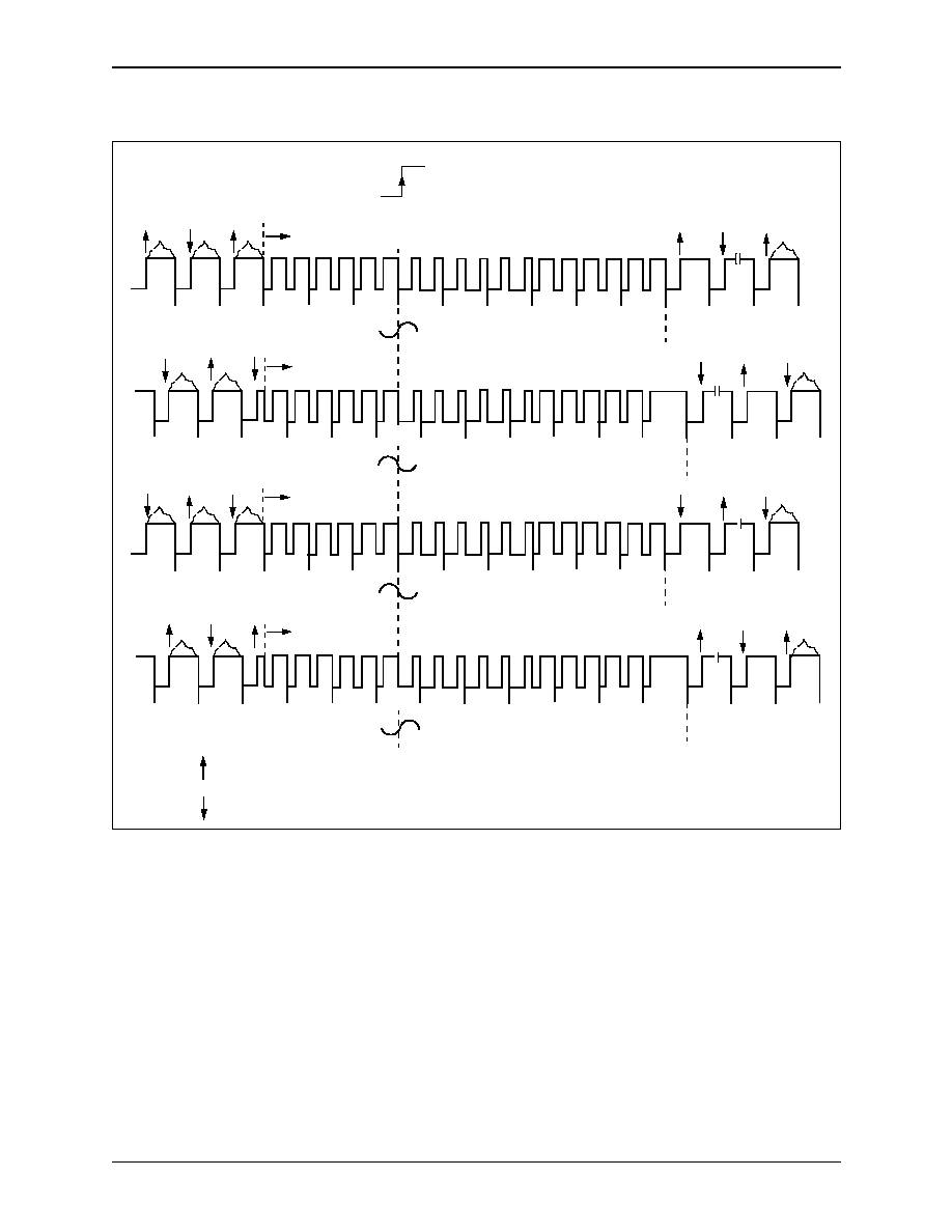
1.0 Functional Description
Bt868/Bt869
1.3 Circuit Description
Flicker-Free Video Encoder with Ultrascale
TM
Technology
1-22
Conexant
100123B
Figure 1-5. Interlaced 525-Line (NTSC) Video Timing
NOTE(S):
SMPTE line numbering convention is used rather than CCIR624.
22
7
6
5
4
3
BURST PHASE
2
1
525
524
523
Analog
FIELD 1
Start
of
VSYNC
Analog
FIELD 2
272
271
270
269
268
267
263
262
261
266
265
264
285
Analog
FIELD 3
BURST PHASE
Analog
FIELD 4
Burst Begins with Positive Half-Cycle
Burst Phase = Reference Phase = 180∞ Relative to B≠Y
Burst Begins with Negative Half-Cycle
Burst Phase = Reference Phase = 180∞ Relative to B≠Y
8
9
10
22
7
6
5
4
3
2
1
525
524
523
8
9
10
272
271
270
269
268
267
263
262
261
266
265
264
285
RESET*

Bt868/Bt869
1.0 Functional Description
Flicker-Free Video Encoder with Ultrascale
TM
Technology
1.3 Circuit Description
100123B
Conexant
1-23
Figure 1-6. Interlaced 525-Line (PAL-M) Video Timing
22
7
6
5
4
3
Burst Phase
2
1
525
524
523
Analog
FIELD 1
Start
of
VSYNC*
Analog
FIELD 2
272
271
270
269
268
267
263
262
261
266
265
264
Analog
FIELD 3
Burst Phase
Analog
FIELD 4
8
9
10
7
6
5
4
3
2
1
525
524
523
8
9
272
271
270
269
268
267
263
262
261
266
265
264
Burst Phase = Reference Phase = 135∞ Relative to U
PAL Switch = 0, +V Component
Burst Phase = Reference Phase + 90∞ = 225∞ Relative to U
PAL Switch = 1, ≠V Component
11
12
22
11
12
285
274
273
285
274
273
10
RESET*

1.0 Functional Description
Bt868/Bt869
1.3 Circuit Description
Flicker-Free Video Encoder with Ultrascale
TM
Technology
1-24
Conexant
100123B
Figure 1-7. Interlaced 625-Line (PAL≠B, D, G, H, I, Nc) Video Timing (Fields 1≠4)
24
7
6
5
4
3
≠ U PHASE
2
1
622
621
620
Analog
FIELD 1
Start
of
VSYNC
625
624
623
23
Analog
FIELD 2
337
320
318
317
316
315
314
309
308
312
311
336
319
337
320
317
316
315
314
308
313
312
311
336
319
310
313
309
318
310
24
7
6
5
4
3
2
1
622
621
620
625
624
623
23
FIELD One
FIELD Two
FIELD Three
FIELD Four
Burst
Blanking
Intervals
Burst Phase = Reference Phase = 135∞ Relative to U
PAL Switch = 0, +V Component
Burst Phase = Reference Phase + 90∞ = 225∞ Relative to U
PAL Switch = 1, ≠V Component
Analog
FIELD 3
Analog
FIELD 4
RESET*

Bt868/Bt869
1.0 Functional Description
Flicker-Free Video Encoder with Ultrascale
TM
Technology
1.3 Circuit Description
100123B
Conexant
1-25
Figure 1-8. Interlaced 625-Line (PAL≠B, D, G, H, I, Nc) Video Timing (Fields 5≠8)
24
7
6
5
4
3
≠ U PHASE
2
1
622
621
620
Analog
FIELD 5
Start
of
VSYNC
625
624
623
23
337
320
318
317
316
315
314
309
308
312
311
336
319
337
320
317
316
315
314
308
313
312
311
336
319
310
313
309
318
310
24
7
6
5
4
3
2
1
622
621
620
625
624
623
23
FIELD Five
FIELD Six
FIELD Seven
FIELD Eight
Burst
Blanking
Intervals
Burst Phase = Reference Phase = 135∞ Relative to U
PAL Switch = 0, +V Component
Burst Phase = Reference Phase + 90∞ = 225∞ Relative to U
PAL Switch = 1, ≠V Component
Analog
FIELD 6
Analog
FIELD 7
Analog
FIELD 8
RESET*
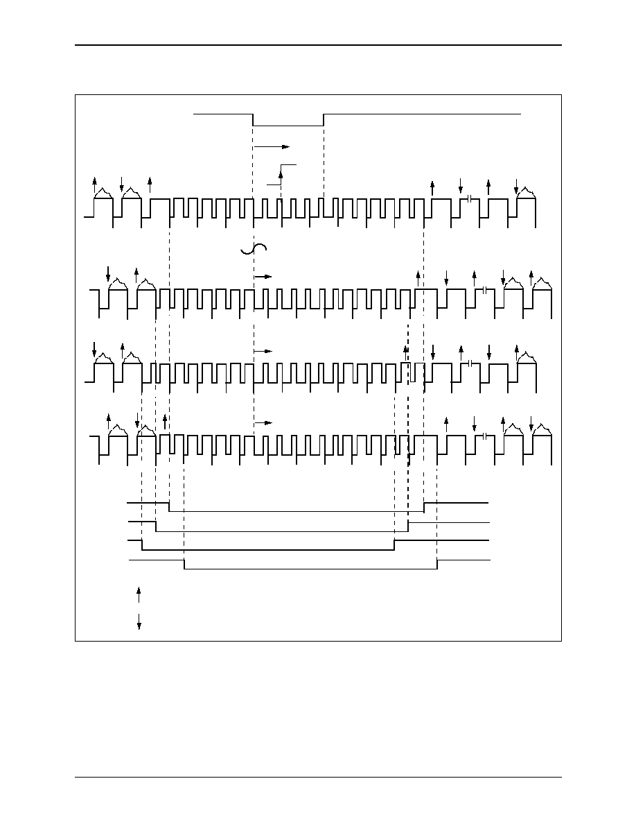
1.0 Functional Description
Bt868/Bt869
1.3 Circuit Description
Flicker-Free Video Encoder with Ultrascale
TM
Technology
1-26
Conexant
100123B
Figure 1-9. Interlaced 625-Line (PAL≠N) Video Timing (Fields 1≠4)
24
7
6
5
4
3
2
1
622
621
620
625
624
623
23
337
320
318
317
316
315
314
309
308
312
311
336
337
320
317
316
315
314
308
313
312
311
336
24
7
5
4
3
2
1
621
620
625
624
623
23
≠ U PHASE
Analog
FIELD 1
Analog
FIELD 2
FIELD One
FIELD Two
FIELD Three
FIELD Four
Burst
Blanking
Intervals
Burst Phase = Reference Phase = 135∞ Relative to U
PAL Switch = 0, +V Component
Burst Phase = Reference Phase + 90∞ = 225∞ Relative to U
PAL Switch = 1, ≠V Component
Analog
FIELD 3
Analog
FIELD 4
RESET*
VSYNC*
310
309
622
310
313
319
6
318
319

Bt868/Bt869
1.0 Functional Description
Flicker-Free Video Encoder with Ultrascale
TM
Technology
1.3 Circuit Description
100123B
Conexant
1-27
Figure 1-10. Interlaced 625-Line (PAL≠N) Video Timing (Fields 5≠8)
24
7
6
5
4
3
≠ U PHASE
2
1
622
621
620
625
624
623
23
337
320
318
317
316
315
314
309
308
312
311
336
319
337
320
317
316
315
314
308
313
312
311
336
319
310
313
309
318
310
24
7
6
5
4
3
2
1
622
621
620
625
624
623
23
FIELD Five
FIELD Six
FIELD Seven
FIELD Eight
Burst
Blanking
Intervals
Burst Phase = Reference Phase = 135∞ Relative to U
PAL Switch = 0, +V Component
Burst Phase = Reference Phase + 90∞ = 225∞ Relative to U
PAL Switch = 1, ≠V Component
Analog
FIELD 6
Analog
FIELD 7
Analog
FIELD 8
Analog
FIELD 5
VSYNC*

1.0 Functional Description
Bt868/Bt869
1.3 Circuit Description
Flicker-Free Video Encoder with Ultrascale
TM
Technology
1-28
Conexant
100123B
Figure 1-11. Noninterlaced 262-Line (NTSC) Video Timing
10
21
9
8
7
6
5
4
3
FIELD 1
2
1
262
261
START
of
VSYNC
263
524
523
268
267
266
265
264
272
271
270
269
Burst Begins with Positive Half-Cycle
Burst Phase = Reference Phase = 180∞ Relative to B-Y
Burst Begins with Negative Half-Cycle
Burst Phase = Reference Phase = 180∞ Relative to B-Y
285
START
of
VSYNC
FIELD 2
Figure 1-12. Noninterlaced 262-Line (PAL≠M) Video Timing
Burst Begins with Positive Half-Cycle
Burst Phase = Reference Phase = 180∞ Relative to B-Y
Burst Begins with Negative Half-Cycle
Burst Phase = Reference Phase = 180∞ Relative to B-Y
10
21
9
8
7
6
5
4
3
285
272
271
270
269
268
267
2
1
525
524
START
of
VSYNC
266
265
264
263
262
274
11
12
273
FIELD 1
FIELD 2
START
of
VSYNC

Bt868/Bt869
1.0 Functional Description
Flicker-Free Video Encoder with Ultrascale
TM
Technology
1.3 Circuit Description
100123B
Conexant
1-29
1.3.23 Subcarrier Generation
The device uses a 32-bit-word to synthesize the subcarrier. The value of the
subcarrier increment required to generate the desired subcarrier frequency is
found with the following equation:
MSC[31:0] = (int) (2
32
*
F
sc
/ F
clk
+ 0.5)
or more directly, for NTSC:
MSC[31:0] = 2
32
*
[455
*
/ (2
*
H_CLKO)]
and for PAL:
MSC[31:0] = 2
32
*
[(1135/4 + 1/625) / (H_CLKO)]
where F
clk
is the encoder clock rate. This allows the generation of any desired
subcarrier to enable the generation of any desired video standard. The 32-bit
subcarrier increment MSC[31:0] must be loaded by the serial interface before the
subcarrier can be enabled. The device is reset to disable chroma until the last byte
of the 32-bit increment is loaded, at which time the chroma will be enabled, unless
the DCHROMA bit is set.
In order to prevent any residual errors from accumulating, the subcarrier DTO
(Discrete Time Oscillator) is reset every four fields for NTSC formats and every
eight fields for PAL formats.
Figure 1-13. Noninterlaced 312-Line (PAL≠B, D, G, H, I, N, Nc) Video Timing
23
7
6
5
1
312
311
310
309
308
Start
of
VSYNC
2
3
4
RESET*
24
23
7
6
5
1
312
311
310
309
308
2
3
4
24
Burst Phase = Reference Phase = 135∞ Relative to U
PAL Switch = 0, +V Component
Burst Phase = Reference Phase + 90∞ = 225∞ Relative to U
PAL Switch = 1, ≠V Component

1.0 Functional Description
Bt868/Bt869
1.3 Circuit Description
Flicker-Free Video Encoder with Ultrascale
TM
Technology
1-30
Conexant
100123B
1.3.24 Burst Generation
The subcarrier burst generation is a function of the video standard (e.g. NTSC or
PAL), the subcarrier frequency increment (MSC[31:03]), and the burst horizontal
begin and end register settings (HBURST_BEGIN[7:0] and
HBURST_END[7:0]). The value of HBURST_BEGIN[7:0] and
HBURST_END[7:0] is the desired pixel minus a value of 128. The burst will
automatically be blanked during the horizontal sync to prevent invalid sync pulses
from being generated. The burst blanking is automatically controlled by the
selected video format. The burst rise and fall times are automatically generated by
the device.
The burst amplitude can be programmed by BST_AMP[5:0].
Table 1-8
shows
the ranges of burst values obtainable and the preferred values for various video
formats.
1.3.25 Chrominance Disable
The chrominance subcarrier can be turned off by setting the DCHROMA bit to a
logical 1. This kills burst as well, providing luminance-only signals on the CVBS
output and a static blank level on the C/R output.
1.3.26 Digital Processing
Once the input data is converted into internal YUV format, the UV components
are low-pass filtered with a filter response illustrated in
Figure 1-14
(linearly
scalable by clock frequency). The Y and filtered UV components are upsampled
to CLK frequency by a digital filter whose response is illustrated in
Figure 1-15
.
Figure 1-14. Three-Stage Chroma Filter
5
0
≠ 5
≠ 15
≠ 20
≠ 25
≠ 30
≠ 35
≠ 40
≠ 10
Frequency MHz
A
t
t
e
n
uat
ion dB
0
0.5
1
1.5
2
CLK = 27 MHz

Bt868/Bt869
1.0 Functional Description
Flicker-Free Video Encoder with Ultrascale
TM
Technology
1.3 Circuit Description
100123B
Conexant
1-31
1.3.27 Subcarrier Phasing
In order to maintain correct SC-H phasing, subcarrier phase is set to 0 on the
leading edge of the analog vertical sync every four (NTSC) or eight (PAL) fields,
unless the DIS_SCRESET bit is set to a logical 1. This is true for both interlaced
and non-interlaced outputs. The subcarrier phase can be adjusted from the
nominal 0 phase by the PHASE_OFF[7:0] register, where each LSB change
corresponds to a 360/256 degree change in the phase.
Setting DIS_SCRESET to 1 may be useful in situations where the ratio of
CLK/2 to HSYNC* edges in a color frame is noninteger, which could produce a
significant phase impulse by resetting to 0.
1.3.28 Noninterlaced Operation
When the Bt868/869 is programmed for noninterlaced master mode, it always
displays the odd field. FIELD will change state on the leading edge of the analog
vertical sync. A 30 Hz offset should be subtracted from the color subcarrier
frequency while in NTSC mode so that the color subcarrier phase will be inverted
from field to field. Transition from interlaced to noninterlaced in master mode
occurs during odd fields to prevent synchronization disturbance.
NOTE:
Consumer VCRs can record noninterlaced video with minor noise
artifacts, but special effects (e.g., scan > 2x) may not function properly.
Figure 1-15. Luminance Upsampling Filter Response
5
0
≠ 5
≠ 15
≠ 20
≠ 25
≠ 30
≠ 35
≠ 40
≠ 10
Frequency MHz
A
t
t
e
n
uat
ion dB
0
6
12
2
4
8
10
(Internal Encoder CLK = 27 MHz)

1.0 Functional Description
Bt868/Bt869
1.3 Circuit Description
Flicker-Free Video Encoder with Ultrascale
TM
Technology
1-32
Conexant
100123B
1.3.29 Closed Captioning
The Bt868/869 encodes NTSC/PAL≠M closed captioning on scan line 21, and
NTSC/PAL≠M extended data services on scan line 284. Four 8-bit registers
(CCF1B1, CCF1B2, CCF2B1, and CCF2B2) provide the data while bits ECCF1
and ECCF2 enable display of the data. A logical 0 corresponds to the blanking
level of 0 IRE, while a logical 1 corresponds to 50 IRE above the blanking level.
Closed captioning for PAL≠B, D, G, H, I, N, Nc is similar to that for NTSC.
Closed-caption (CC) encoding is performed for 625-line systems according to the
system proposed by the National Captioning Institute; clock and data timing is
identical to that of NTSC system, except that encoding is provided on lines 22
and 335, for closed captioning and extended data services respectively.
The Bt868/869 generates the clock run-in and appropriate timing
automatically. Pixel inputs are ignored during CC encoding. See FCC Code of
Federal Regulations (CFR) 47 Section 15.119 (10/91 edition or later) for
programming information. EIA608 describes ancillary data applications for Field
2 Line 21 (line 284).
When CCF1B2 is written, CCSTAT_O is set; when CCF2B2 is written,
CCSTAT_E is set. After the CC bytes for the odd field are encoded, CCSTAT_O
is cleared; after the CC bytes for the even field are encoded, CCSTAT_E is
cleared. If the ECCGATE bit is set, no further encoding will be performed until
the appropriate registers are again written; a null will be transmitted on the
appropriate CC line in that case. If the ECCGATE bit is not set, the user must
rewrite the CC registers prior to reaching the CC line; otherwise the last bytes will
be re-encoded. The CC data bytes are double-buffered to prevent loss of data
during the encoding process.
1.3.30 Internal Color Bars
The Bt868/869 can be configured to generate 100% amplitude, 75% saturation
(100/7.5/75/7.5 for NTSC/PAL-M with setup, 100/0/75/0 for PAL) color bars.
Color bars can be enabled or disabled by setting the ECBAR bit to a logical 1. The
device uses the H_BLANKO register value to determine the starting point of the
color bars, and the H_ACTIVE register value to determine the width. Eight bars
are displayed, with the colors and amplitudes being generated internally. The pixel
inputs are ignored in color bar mode. The MY, MCR, and MCB registers must be
programmed for RGB inputs prior to color bar operation.
1.3.31 Macrovision Encoding
The Bt869 device supports Version 7.xx of the Macrovision specification for
copy protection for all NTSC and PAL modes. The Bt868 does not support the
Macrovision feature.

Bt868/Bt869
1.0 Functional Description
Flicker-Free Video Encoder with Ultrascale
TM
Technology
1.3 Circuit Description
100123B
Conexant
1-33
1.3.32 Outputs
There are four modes for the analog outputs, selected by OUT_MODE[1:0]. The
first mode (OUT_MODE=0) generates Composite video (CVBS), Luma (Y),
Chroma (C), and Delayed Luma (Y_DLY). The second mode (OUT_MODE=1)
generates Luma-Delayed Composite video (CVBS_DLY), Luma (Y), Chroma
(C), and Delayed Luma (Y_DLY). The third mode (OUT_MODE=2) generates
Component YUV and Delayed Luma (Y_DLY). The fourth mode
(OUT_MODE=3) generates VGA-style RGB outputs. The LUMADLY[1:0]
register bits control the amount of delay for the delayed luma, from 0 to 3 pixel
clocks. For each mode, any of the four generated outputs can be muxed to any of
three output DACs by the register bits OUT_MUXA[1:0], OUT_MUXB[1:0],
and OUT_MUXC[1:0]. All digital-to-analog converters are designed to drive
standard video levels into a combined RLOAD of 37.5
(doubly-terminated
75
). Unused outputs should be disabled by setting the corresponding
DACDISX bit to minimize supply current, or connected directly to ground to
minimize supply switching currents.
1.3.33 Output Connection Status
The device can determine whether or not the DAC output is connected to a
monitor by verifying that the output is doubly-terminated. The MONSTATx bit
for the corresponding DAC is set to a 1 if the device senses a doubly-terminated
load on a reset condition or if the CHECK_STAT register bit is set. While
CHECK_STAT is set, the output is forced to 2/3 of VREF when terminated and
4/3 of VREF if unterminated. The MONSTATx bit reflects the condition when the
DAC output is less than or equal to VREF. The CHECK_STAT bit is
automatically cleared after two clock cycles.
1.3.34 Output Filtering and SINX/X Compensation
The DAC output response is a typical sinx/x response. For the composite video
output, this results in a slightly lower than desired burst and chroma amplitude
value. This can be compensated for, to some extent, by choosing an output filter
which boosts higher frequency response slightly. Another method which can be
used effectively, and is used by default in the auto configuration modes, is to
boost the burst and chroma gain as programmed by the BST_AMP and
MCR/MCB register values by x/sinx. The amount of sinx/x amplitude reduction
is calculated by:
sinx/x = sin (
*
Fsc/Fclk) / (
*
Fsc/Fclk)

1.0 Functional Description
Bt868/Bt869
1.3 Circuit Description
Flicker-Free Video Encoder with Ultrascale
TM
Technology
1-34
Conexant
100123B
1.3.35 Power-Down Modes
The device can be placed in a low-power mode by the SLEEP pin. In this mode,
the analog circuitry is shut down, disabling the output video, and the internal
clock to the device is held constant, placing both the analog and digital current
draw to a minimum. Register states are preserved, but other chip functionality
(including the serial interface) is disabled. This mode achieves the greatest
reduction in power.
In addition, the entire analog subsection can be powered-down with the
DACOFF bit, allowing digital operations to continue while reducing the power in
the analog circuitry. This will achieve a significant reduction in power while
maintaining all digital functionality. Each individual DAC can also be powered
down by its corresponding DACDISx bit. This is useful only if some of the DACs
are being used, in order to minimize the power in the system.
1.3.36 Serial Interface
The device includes a 2-wire serial interface which is used for programming the
registers in the device. The interface is designed to operate with either 3.3 V or
5 V input levels by changing the supply voltage for the input and output drivers
with the VDD_SI pin.

100123B
Conexant
2-1
2
2.0 Internal Registers
A register bit map is displayed in
Table 2-1
, and a read-back bit map is displayed
in
Table 2-2
. Bit descriptions and detailed programming information follow the
bit map. All registers are write-only and are set to 0 following a software reset. A
software reset is always performed at power-up; after power-up, a reset can be
triggered by writing the SRESET register bit.
Table 2-1. Register Bit Map (1 of 3)
8-Bit
Address
D7
D6
D5
D4
D3
D2
D1
D0
6C
TIMING RESET
RESERVED
6E
HSYNOFFSET[7:0]
70
HSYNOFFSET[9:8]
HSYNWIDTH[5:0]
72
VSYNOFFSET[7:0]
74
DATDLY
DATSWP
VSYNOFFSET[10:8]
VSYNWIDTH[2:0]
76
H_CLKO[7:0]
78
H_ACTIVE[7:0]
7A
HSYNC_WIDTH[7:0]
7C
HBURST_BEGIN[7:0]
7E
HBURST_END[7:0]
80
H_BLANKO[7:0]
82
V_BLANKO[7:0]
84
V_ACTIVEO[7:0]
86
V_ACTIVEO[8]
Reserved
H_ACTIVE[9:8]
H_CLKO[11:8]
88
H_FRACT[7:0]
8A
H_CLKI[7:0]
8C
H_BLANKI[7:0]
8E
Reserved
Reserved
Reserved
VBLANKDLY
H_BLANKI[8]
H_CLKI[10:8]
90
V_LINESI[7:0]
92
V_BLANKI[7:0]
94
V_ACTIVEI[7:0]
96
CLPF[1:0]
YLPF[1:0]
V_ACTIVEI[9:8]
V_LINESI[9:8]

2.0 Internal Registers
Bt868/Bt869
Flicker-Free Video Encoder with Ultrascale
TM
Technology
2-2
Conexant
100123B
98
V_SCALE[7:0]
9A
H_BLANKO[9:8]
V_SCALE[13:8]
9C
PLL_FRACT[7:0]
9E
PLL_FRACT[15:8]
A0
EN_XCLK
BY_PLL
PLL_INT[5:0]
A2
Reserved
ECLIP
PAL_MD
DIS_SCRESET
VSYNC_DU
R
625LINE
SETUP
NI_OUT
A4
SYNC_AMP[7:0]
A6
BST_AMP[7:0]
A8
MCR[7:0]
AA
MCB[7:0]
AC
MY[7:0]
AE
MSC[7:0]
B0
MSC[15:8]
B2
MSC[23:16]
B4
MSC[31:24]
B6
PHASE_OFF[7:0]
B8
EN_PINCFG
CONFIG[2:0]
BA
SRESET
CHECK_STAT SLAVER
DACOFF
Reserved
DACDIS
C
DACDISB
DACDISA
BC
CCF2B1[7:0]
BE
CCF2B2[7:0]
C0
CCF1B1[7:0]
C2
CCF1B2[7:0]
C4
ESTATUS[1:0]
ECCF2
ECCF1
ECCGATE
ECBAR
DCHROM
A
EN_OUT
C6
EN_BLANKO
EN_DOT
FIELDI
VSYNCI
HSYNCI
IN_MODE[2:0]
C8
DIS_YFLPF
DIS_FFILT
F_SELC[2:0]
F_SELY[2:0]
CA
DIS_GMUSHY
DIS_GMSHY
YCORING[2:0]
YATTENUATE[2:0]
CC
DIS_GMUSHC
DIS_GMSHC
CCORING[2:0]
CATTENUATE[2:0]
CE
Reserved
OUT_MUXC[1:0]
OUT_MUXB[1:0]
OUT_MUXA[1:0]
D0
CCR_START[7:0]
D2
CC_ADD[7:0]
D4
MODE2X
DIV2
EN_ASYNC
CCR_START[8] CC_ADD[11:8]
Table 2-1. Register Bit Map (2 of 3)
8-Bit
Address
D7
D6
D5
D4
D3
D2
D1
D0

Bt868/Bt869
2.0 Internal Registers
Flicker-Free Video Encoder with Ultrascale
TM
Technology
2.1 Essential Registers
100123B
Conexant
2-3
2.1 Essential Registers
The power-up state is defined to be black burst CCIR601 NTSC video. To enable
active video, the EN_OUT register bit must be set. This bit enables CLKO,
HSYNC*, VSYNC*, BLANK*, and FIELD outputs. If this bit is not set, then
these pins are set to a high impedance.
2.2 Writing Addresses
Following a start condition, writing 0x88 initiates access to subaddresses.
Alternative address 0x8A must be written if the ALTADDR pin is high. If the data
is written in subaddress order, only the beginning subaddress needs to be written;
the internal address counter will automatically increment after each write to a
register.
2.3 Reading Information
Following a start condition, writing 0x89 initiates the read-back sequence, during
which 8 bits of information can be read from the SID pin, MSB first. Alternative
address 0x8B is required if the ALTADDR pin is high. For the case of
ESTATUS[1:0]=00 prior to the read sequence, the first three bits indicate the part
type (Bt868 or Bt869). The lower five bits indicate the version number or the
status bits. The instances where ESTATUS[1:0]=01 and ESTATUS[1:0]=10, the
bits read back from the VGA Encoder will contain information as specified by
Table 2-2
.
For software detection of a connected TV monitor on each DAC output,
ESTATUS[1:0] must equal 01 and the MONSTAT x bits should be read
accordingly after writing to CHECK_STAT.
Data details are defined in
Table 2-3
; bit and register definitions are displayed
in
Table 2-4
.
D6
Reserved
Reserved
Reserved
Reserved
OUT_MODE[1:0]
LUMADLY[1:0]
D8
Reserved
Table 2-1. Register Bit Map (3 of 3)
8-Bit
Address
D7
D6
D5
D4
D3
D2
D1
D0

2.0 Internal Registers
Bt868/Bt869
2.3 Reading Information
Flicker-Free Video Encoder with Ultrascale
TM
Technology
2-4
Conexant
100123B
Table 2-2. Read-Back Bit Map
ESTATUS[1:0]
7
6
5
4
3
2
1
0
00
ID[2:0]
VERSION[2:0]
01
MONSTAT_
A
MONSTAT_B
MONSTAT_C
CCSTAT_E
CCSTAT_O
FIELD[2:0]
10
PLL_LOCK
FIFO_OVER
FIFO_UNDER
PAL
BUSY
Table 2-3. Data Details Defined
Bit Names
Data Definition
ID[2:0]
Indicates the part number: 000 is returned from the Bt868; 001 is returned from the Bt869.
VERSION[4:0]
Version number; for this revision, these bits are 00001.
MONSTAT_A
Monitor connection status for DACA output, 1 denotes monitor connected to DACA.
MONSTAT_B
Monitor connection status for DACB output, 1 denotes monitor connected to DACB.
MONSTAT_C
Monitor connection status for DACC output, 1 denotes monitor connected to DACC.
CCSTAT_E
High if closed-caption data has been written for the even field; it is low immediately after the clock run-in on
line 21(NTSC) or 22(PAL).
CCSTAT_O
High if closed-caption data has been written for the odd field; it is low immediately after the clock run-in on
line 284(NTSC) or 335(PAL).
FIELD[2:0]
Field number, where 000 indicates the first field, 111 indicates the 8th field.
PLL_LOCK
High when PLL is locked.
FIFO_OVER
Set to one if FIFO overflows. Reset on read.
FIFO_UNDER
Set to one if FIFO underflows. Reset on read.
PAL
Indicates status of PAL pin.
BUSY
Indicates that the device is in the process of initializing the registers and that the registers cannot be written.
This bit remains high for 512 CLK-0 after an auto configuration cycle begins.
Table 2-4. Programming Detail (1 of 7)
Bit/Register Names
Bit/Register Definition
H_CLKO[11:0]
Number of output CLKs/line
H_ACTIVE[9:0]
Number of active input and output pixels
HSYNC_WIDTH[7:0]
Analog sync width in clocks
HBURST_BEGIN[7:0]
Beginning of burst 50% point in number of clock cycles from analog hsync falling edge
HBURST_END[7:0]
End of burst 50% point in number of clock cycles--128 from analog sync falling edge
H_BLANKO[9:0]
Number of output CLKs between leading edge of horizontal sync and active video
V_BLANKO[7:0]
Line number of first active line (number of blank lines + 1)
V_ACTIVEO[8:0]
Number of active output lines/field

Bt868/Bt869
2.0 Internal Registers
Flicker-Free Video Encoder with Ultrascale
TM
Technology
2.3 Reading Information
100123B
Conexant
2-5
H_FRACT[7:0]
Fractional number of input clocks per line
H_CLKI[10:0]
Number of clocks per line between successive HSYNC* edges
H_BLANKI[8:0]
Number of input pixels between HSYNC* leading edge and first active pixel
VBLANKDLY
If set, the effective vertical blanking value in the second field is V_BLANKI+1.
V_LINESI[9:0]
Number of vertical input lines
V_BLANKI[7:0]
Number of input lines between VSYNC* leading and first active line
V_ACTIVEI[9:0]
Number of active input lines
CLPF[1:0]
Chroma Horizontal Low Pass Filter
00 = Bypass
01 = Reserved
10 = Chroma Horizontal LPF2
11 = Chroma Horizontal LPF3
YLPF[1:0]
Luma Post-FlickerFilter/Scaler Horizontal Low Pass Filter
00 = Bypass
01 = Luma Horizontal LPF1
10 = Luma Horizontal LPF2
11 = Luma Horizontal LPF3
V_SCALE[13:0]
Vertical scaling coefficient
PLL_FRACT[15:0]
Fractional portion of PLL multiplier
PLL_INT[5:0]
Integer portion of PLL multiplier
EN_XCLK
0 = Encoder generates pixel clock
1 = Use CLKI pin as pixel clock source
BY_PLL
0 = Use PLL
1 = Bypass PLL (encoder clock is crystal frequency)
Reserved
Reserved for future software compatibility; should be set to zero for normal operation.
ECLIP
0 = Normal operation
1 = Enable clipping; DAC values less than 31 are made 31
PAL_MD
Video output switch bit. If PAL pin = 0, this controls analog output format
0 = Changes video output to NTSC mode
1 = Changes video output to PAL mode (even if PAL pin = 0)
DIS_SCRESET
0 = Normal operation. The subcarrier phase is reset to 0 at the beginning of each color field
sequence
1 = Disables subcarrier reset event at beginning of field sequence
VSYNC_DUR
0 = Generates 2.5-line VSYNC analog output
1 = Generates 3-line VSYNC analog output
625LINE
0 = 525-line format
1 = 625-line format
SETUP
1 = Setup on. The 7.5≠IRE setup is enabled for active video lines.
0 = Setup off. The 7.5≠IRE setup is disabled for active video lines.
NI_OUT
0 = Interlaced analog video output
1 = Noninterlaced analog video output
Table 2-4. Programming Detail (2 of 7)
Bit/Register Names
Bit/Register Definition

2.0 Internal Registers
Bt868/Bt869
2.3 Reading Information
Flicker-Free Video Encoder with Ultrascale
TM
Technology
2-6
Conexant
100123B
SYNC_AMP[7:0]
Multiplication factor for sync amplitude
BST_AMP[7:0]
Burst amplitude multiplication factor
MCR[7:0]
Multiplication factor for CR (or R-Y) component prior to subcarrier modulation
MCB[7:0]
Multiplication factor for CB (or B-Y) component prior to subcarrier modulation
MY[7:0]
Multiplication factor for Y component
MSC[31:0]
Subcarrier increment
PHASE_OFF[7:0]
Subcarrier phase offset
EN_PINCFG
When set, this will enable the auto configuration to be controlled by P[23:21]. Whenever a change
is detected on these pins, the mode is reconfigured.
This field determines the configuration for the automatic configuration process
CONFIG[2:0]
000 = NTSC 640x480 RGB input
001 = PAL 640x480 RGB input
010 = NTSC 800x600 RGB input
011 = PAL 800x600 RGB input
100 = NTSC 640x480 YCrCb input
101 = PAL 640x480 YCrCb input
110 = NTSC 800x600 YCrCb input
111 = PAL 800x600 YCrCb input
SRESET
Writing a 1 to this bit performs a software reset; all registers are reset to 0s unless the
CONFIG[2:0] field is non-0; in that case, the automatic configuration process is begun and the
BUSY status bit is set. This bit is automatically cleared.
CHECK_STAT
Writing a 1 to this bit checks the status of the monitor connections at the DAC output. This is also
automatically performed on any reset condition, including a software reset. This bit is automatically
cleared.
DACOFF
0 = Normal operation
1 = Disables DAC output current and internal voltage reference. This will limit power consumption
to just the digital circuits.
DACDISC
0 = Normal operation
1 = Disables DAC output. Current is set to 0; output will go to 0 V.
DACDISB
0 = Normal operation
1 = Disables DACB output. Current is set to 0; output will go to 0 V.
DACDISA
0 = Normal operation
1 = Disables DACA output. Current is set to 0; output will go to 0 V.
CCF2B1[7:0]
This is the first byte of closed-caption information for the even field, line 284 for NTSC or line 335
for PAL. Data is encoded LSB first.
CCF2B2[7:0]
This is the second byte of closed-caption information for the even field, line 284 for NTSC or line
335 for PAL. Data is encoded LSB first.
CCF1B1[7:0]
This is the first byte of closed-caption information for the odd field, line 21 for NTSC or line 22 for
PAL. Data is encoded LSB first.
CCF1B2[7:0]
This is the second byte of closed-caption information for the odd field, line 21 for NTSC or line 22
for PAL. Data is encoded LSB first.
ESTATUS[1:0]
Serial read-back status bit selection. (See
Table 2-2
.)
Table 2-4. Programming Detail (3 of 7)
Bit/Register Names
Bit/Register Definition

Bt868/Bt869
2.0 Internal Registers
Flicker-Free Video Encoder with Ultrascale
TM
Technology
2.3 Reading Information
100123B
Conexant
2-7
ECCF2
0 = Disables closed-caption encoding on field 2.
1 = Enables closed-caption encoding on field 2.
ECCF1
0 = Disables closed-caption encoding on field 1.
1 = Enables closed-caption encoding on field 1.
ECCGATE
0 = Normal closed-caption encoding.
1 = Enables closed-caption encoding constraints. After encoding, future encoding is disabled until
a complete pair of new data bytes is received. This prevents encoding of redundant or
incomplete data.
ECBAR
0 = Normal operation
1 = Enables color bars.
DCHROMA
0 = Normal operation
1 = Blank chroma
EN_OUT
0 = Three-states all outputs.
1 = Allows outputs to be enabled (depending upon EN_BLANKO register bit and SLAVE pin).
EN_BLANKO
Enables BLANK* pin as an output.
EN_DOT
Enables dot clock synchronization on BLANK* pin.
FIELDI
0 = Logical 1 on FIELD indicates an even field.
1 = Logical 1 on FIELD indicates an odd field.
VSYNCI
0 = Active low VSYNC*
1 = Active high VSYNC*
HSYNCI
0 = Active low HSYNC*
1 = Active high HSYNC*
IN_MODE[2:0]
Format of pixels at input of encoder:
000 = 24-bit RGB multiplexed
001 = 16-bit RGB multiplexed
010 = 15-bit RGB multiplexed
011 = 24-bit RGB non-multiplexed
100 = 24-bit YCrCb multiplexed
101 = 16-bit YCrCb multiplexed
110 = Reserved
111 = 24-bit YCrCb non-multiplexed
DIS_YFLPF
Luma Initial Horizontal Low Pass Filter
0 = Enable
1 = Disable
DIS_FFILT
0 = Enables FlickerFilter
1 = Disables FlickerFilter
F_SELC[2:0]
Chroma FlickerFilter:
000 = 5 Line
001 = 2 Line
010 = 3 Line
011 = 4 Line
100 = Alternate 5 Line
101 = Alternate 5 Line
110 = Alternate 5 Line
111 = Alternate 5 Line
Table 2-4. Programming Detail (4 of 7)
Bit/Register Names
Bit/Register Definition

2.0 Internal Registers
Bt868/Bt869
2.3 Reading Information
Flicker-Free Video Encoder with Ultrascale
TM
Technology
2-8
Conexant
100123B
F_SELY[2:0]
Luma FlickerFilter:
000 = 5 Line
001 = 2 Line
010 = 3 Line
011 = 4 Line
100 = Alternate 5 Line
101 = Alternate 5 Line
110 = Alternate 5 Line
111 = Alternate 5 Line
DIS_GMUSHY
0 = Enables Luma Anti-Psuedo Gamma Removal.
1 = Disables Luma Anti-Psuedo Gamma Removal.
DIS_GMSHY
0 = Enables Luma Psuedo Gamma Removal.
1 = Disables Luma Psuedo Gamma Removal.
YCORING[2:0]
Luma Coring:
000 = Bypass
001 = 1/128 of range
010 = 1/64 of range
011 = 1/32 of range
100 = 1/16 of range
101 = 1/8 of range
110 = 1/4 of range
111 = Reserved
YATTENUATE[2:0]
Luma Attenuation
000 = 1.0 gain (no attenuation)
001 = 15/16 gain
010 = 7/8 gain
011 = 3/4 gain
100 = 1/2 gain
101 = 1/4 gain
110 = 1/8 gain
111 = 0 gain (Force Luma to 0)
DIS_GMUSHC
0 = Enables Chroma Anti-Psuedo Gamma Removal.
1 =Disables Chroma Anti-Psuedo Gamma Removal.
DIS_GMSHC
0 = Enables Chroma Psuedo Gamma Removal.
1 = Disables Chroma Psuedo Gamma Removal.
CCORING[2:0]
Chroma Coring:
000
=
Bypass
001 = 1/128 of range (+/- 1/256 of range)
010 = 1/64 of range (+/- 1/128 of range)
011 = 1/32 of range (+/- 1/64 of range)
100 = 1/16 of range (+/- 1/32 of range)
101 = 1/8 of range (+/- 1/16 of range)
110 = 1/4 of range (+/- 1/8 of range)
111 = Reserved
Table 2-4. Programming Detail (5 of 7)
Bit/Register Names
Bit/Register Definition

Bt868/Bt869
2.0 Internal Registers
Flicker-Free Video Encoder with Ultrascale
TM
Technology
2.3 Reading Information
100123B
Conexant
2-9
CATTENUATE[2:0]
Chroma Attenuation:
000 = 1.0 gain (No Attenuation)
001 = 15/16 gain
010 = 7/8 gain
011 = 3/4 gain
100 = 1/2 gain
101 = 1/4 gain
110 = 1/8 gain
111 = 0 gain (Force Chroma to 0)
OUT_MUXA[1:0]
00 = Output Video[0] on DACA
01 = Output Video[1] on DACA
10 = Output Video[2] on DACA
11 = Output Video[3] on DACA
OUT_MUXB[1:0]
00 = Output Video[0] on DACB
01 = Output Video[1] on DACB
10 = Output Video[2] on DACB
11 = Output Video[3] on DACB
OUT_MUXC[1:0]
00 = Output Video[0] on DACC
01 = Output Video[1] on DACC
10 = Output Video[2] on DACC
11 = Output Video[3] on DACC
CCR_START[8:0]
Closed-captioning clock run-in start in clock cycles from leading edge of HSYNC*
CC_ADD[11:0]
Closed-captioning DTO increment
DIV2
Divides input pixel rate by two (for CCIR601 interlaced timing input.
MODE2X
Divides selected input clock by two (allows for 2x rather than double-edge clock input).
EN_ASYNC
Set to 0 for normal operation.
OUT_MODE[1:0]
00 = Video[0-3] is CVBS/ Y/ C/ Y_DLY
01 = Video[0-3] is CVBS_DLY/ Y/ C/ Y_DLY
10 = Video[0-3] is V/ Y/ U/ Y_DLY
11 = Video[0-3] is R/ G/ B/ X (VGA mode)
LUMADLY[1:0]
This 2-bit value can be used to program the luminance delay in pixels for the CVBS_DLY and
Y_DLY output modes.
00 = No delay
01 = 1 pixel
10 = 2 pixels
11 = 3 pixels
HSYNOFFSET[9:0]
A 2s-complement number. The values range from ≠512 pixels to +511 pixels. This register manip-
ulates the falling edge position of the digital HSYNC output from Bt868. The default value is 0 and
denotes the standard position of the HSYNC leading edge.
Table 2-4. Programming Detail (6 of 7)
Bit/Register Names
Bit/Register Definition

2.0 Internal Registers
Bt868/Bt869
2.3 Reading Information
Flicker-Free Video Encoder with Ultrascale
TM
Technology
2-10
Conexant
100123B
VSYNOFFSET[10:0]
A 2s-complement number. The values range from ≠HCLKI pixels to +HCLKI pixels. This register
causes the falling edge position of the Bt868's digital VSYNC output to occur earlier (≠ value) or
later (+) in time compared to the standard position for NTSC or PAL. The default value is 0 and
denotes the standard position of the VSYNC leading edge.
HSYNWIDTH[5:0]
Controls the duration/width of the digital HSYNC output pulse. Value will be hexadecimal and its
units are in terms of pixels. A value of 0 is a disallowed condition. The acceptable range is 2 pixels
to 3F pixels (=63 decimal). The default value is 2.
VSYNWIDTH[2:0]
Controls the width of the VSYNC output pulse. Denotes the number of lines the VSYNC digital sig-
nal remains low on field transitions. Value will be hexadecimal value and its units are in terms of
lines. A value of 0 is a disallowed condition. The acceptable range is 1 line to (2
3
≠1) lines. The
default value is 1.
DATDLY
Delays the falling edge pixel data by 1 full clock period when the falling edge data precedes the ris-
ing edge data. Ensures that the Bt868 moves the falling edge data after the rising edge data. The
correct sequence of rising edge data/falling edge data/rising edge data will then be encoded by
Buteo. The default value for this bit is 0 because most graphics controllers already transmit data in
the expected rising edge data/falling edge data sequence.
DATSWP
Swaps the falling edge pixel data with the rising edge pixel data at the input of the pixel port. The
default value for this bit is 0 which tells the VGA Encoder to expect an order of rising edge data/fall-
ing edge data coming from the graphics controller.
NOTE(S):
VSYNWIDTH, HSYNWIDTH, VSYNOFFSET, and HSYNOFFSET are active only when the Bt868/869 is in the master
timing mode when the encoder outputs HSYNC and VSYNC pulses. In the slave timing mode, these registers are ignored.
VSYNCWIDTH and HSYNCWIDTH should never be set to 0.
Table 2-4. Programming Detail (7 of 7)
Bit/Register Names
Bit/Register Definition

100123B
Conexant
3-1
3
3.0 PC Board Considerations
For optimum performance of the Bt868/869, proper CMOS layout techniques
should be studied in the Bt451/457/458 Evaluation Module Operation and
Measurements Application Note (AN-16), before PC board layout is begun.
The layout should be optimized for lowest noise on the power and ground
planes by providing good decoupling. The trace length between groups of VAA
and GND pins should be as short as possible to minimize inductive ringing.
A well-designed power distribution network is critical to eliminating digital
switching noise. The ground plane must provide a low-impedance return path for
the digital circuits. A PC board with a minimum of four layers is recommended,
with layers 1 (top) and 4 (bottom) for signals, and layers 2 and 3 for ground and
power, respectively.
3.1 Component Placement
Components should be placed as close as possible to the associated pin in order
for traces to be connected point to point. The optimum layout enables the
Bt868/869 to be located close to the power supply connector and the video output
connector. For an illustration, see
Figure 3-1
.
3.2 Power and Ground Planes
For optimum performance, a common digital and analog ground plane and a
common digital and analog power plane are recommended. The power plane
should provide power to all Bt868/869 power pins, reference voltage (Vref)
circuitry, and COMP decoupling.
The Bt868/869 power plane should be connected to the graphics system power
plane (VCC) at a single point through a ferrite bead, as illustrated in Figures 3-1
and
3-2
. This bead should be located within 3 inches of the Bt868/869. The bead
provides resistance to switching currents, acting as a resistor at high frequencies.
A low-resistance bead should be used, such as Ferroxcube 5659065-3B, Fair-Rite
2723021447, or TDK BF45-4001. See
Table 3-1
for a typical parts list for key
passive components and
Figure 3-3
for a schematic diagram of the recommended
layout.

3.0 PC Board Considerations
Bt868/Bt869
3.2 Power and Ground Planes
Flicker-Free Video Encoder with Ultrascale
TM
Technology
3-2
Conexant
100123B
Figure 3-1. Power Plane Illustration
Bt868
Bt decoder
Analog
Oscillator
3VAA-Bt868 o
o VCC3
Ferrite Bead
Clocks
5V
3V
3 V
o VCC3
Data
PCI or AGP Connector
Bracket
4 layer board
plane order:
Signals
GND
PWR
Signals
BOTTOM
TOP

Bt868/Bt869
3.0 PC Board Considerations
Flicker-Free Video Encoder with Ultrascale
TM
Technology
3.2 Power and Ground Planes
100123B
Conexant
3-3
Figure 3-2. Connection Diagram for Output Filters and Other Key Passive Components
(1)
Some modulators may require AC coupling capacitors (10 µF).
VAA
COMP
VBIAS
VREF
GND
C7
C8
C2≠C6
FSADJUST
RSET =
DACA
DACB
DACC
Bt868/869 Power Plane
P
P
P
LPF
LPF
To Video
Connector
Ground
(Power Supply
Connector)
+3.3 V (VCC)
VAA
Schottky Diodes
Schottky Diodes
RF Modulator/CVBS Out
75
TRAP
RF
Modulator
LPF
22 pF
1.8 µH
270 pF
Bt868/869
C10
+
C1
L1
RF Mod/CVBS
RF
330 pF
GND
To Filter
DAC Output
22 pF
1.8 µH
270 pF
330 pF
Audio
82
ZIN = 1 K
75
,
75
, 75 ,
(1)
P
CVBS
C9
Buffer
100
,1%
1%
1%
1%
Table 3-1. Typical Parts List for Key Passive Components
Location
Description
Vendor Part Number
C1≠C9
0.1 µF Ceramic Capacitor
Erie RPE112Z5U104M50V
C10
47 µF Capacitor
Mallory CSR13F476KM
L1
Ferrite Bead≠Surface Mount
Fair-Rite 2743021447
RSET
1% Metal Film Resistor
Dale CMF-55C
TRAP
Ceramic Resonator
Murata TPSx.xMJ or MB2 (where x.x = sound carrier frequency in MHz)
Schottky Diodes
BAT85 (BAT54F Dual) HP 5082-2305 (1N6263) Siemens BAT 64-04 (Dual)
NOTE(S):
Vendor numbers are listed only as a guide. Substitution of devices with similar characteristics will not affect
Bt868/869
performance.

3.0 PC Board Considerations
Bt868/Bt869
3.2 Power and Ground Planes
Flicker-Free Video Encoder with Ultrascale
TM
Technology
3-4
Conexant
100123B
Figure 3-3. Complete Bt868/Bt869 Recommended Layout

Bt868/Bt869
3.0 PC Board Considerations
Flicker-Free Video Encoder with Ultrascale
TM
Technology
3.3 Decoupling
100123B
Conexant
3-5
3.3 Decoupling
3.3.1 Device Decoupling
For optimum performance, all capacitors should be located as close as possible to
the device, and the shortest possible leads (consistent with reliable operation)
should be used to reduce the lead inductance. Chip capacitors are recommended
for minimum lead inductance. Radial lead ceramic capacitors can be substituted
for chip capacitors and are better than axial lead capacitors for self-resonance.
Values are chosen to have self-resonance above the pixel clock.
3.3.2 Power Supply Decoupling
The best power supply performance is obtained with a 0.1
µF ceramic capacitor
decoupling each group of VAA pins and each group of VDD pins to GND. The
capacitors should be placed as close as possible to the device VAA/VDD pins and
GND pins and connected with short, wide traces.
The 47
µF capacitor shown in
Figure 3-2
is for low-frequency power supply
ripple; the 0.1
µF capacitors are for high-frequency power supply noise rejection.
When a linear regulator is used, the proper power-up sequence must be
verified to prevent latchup. A linear regulator is recommended to filter the analog
power supply if the power supply noise is greater than or equal to 200 mV. This is
especially important when a switching power supply is used, and the switching
frequency is close to the raster scan frequency. About 5% of the power supply
hum and ripple noise less than 1 MHz will couple onto the analog outputs.
3.3.3 COMP Decoupling
The COMP pin must be decoupled to the closest VAA pin, typically with a 0.1
µF
ceramic capacitor. Low-frequency supply noise will require a larger value. The
COMP capacitor must be as close as possible to the COMP and VAA pins. A
surface-mount ceramic chip capacitor is preferred for minimal lead inductance.
Lead inductance degrades the noise rejection of the circuit. Short, wide traces will
also reduce lead inductance.
3.3.4 VREF Decoupling
A 0.1
µF ceramic capacitor should be used to decouple this input to GND.
3.3.5 VBIAS Decoupling
A 0.1
µf ceramic capacitor should be used to decouple this output to GND.

3.0 PC Board Considerations
Bt868/Bt869
3.4 Signal Interconnect
Flicker-Free Video Encoder with Ultrascale
TM
Technology
3-6
Conexant
100123B
3.4 Signal Interconnect
3.4.1 Digital Signal Interconnect
The digital inputs to the Bt868/869 should be isolated as much as possible from
the analog outputs and other analog circuitry. Also, these input signals should not
overlay the analog power plane or analog output signals.
Most of the noise on the analog outputs will be caused by excessive edge rates
(less than 3 ns), overshoot, undershoot, and ringing on the digital inputs.
The digital edge rates should not be faster than necessary, as feedthrough
noise is proportional to the digital edge rates. Lower-speed applications will
benefit from using lower-speed logic (3≠5 ns edge rates) to reduce data-related
noise on the analog outputs.
Transmission lines will mismatch if the lines do not match the source and
destination impedance. This will degrade signal fidelity if the line length
reflection time is greater than one-fourth the signal edge time (refer to
Application Notes AN-11 and AN-12). Line termination or line-length reduction
is the solution. For example, logic edge rates of 2 ns require line lengths of less
than 4 inches without use of termination. Ringing can be reduced by damping the
line with a series resistor (30≠300
).
Radiation of digital signals can also be picked up by the analog circuitry. This
is prevented by reducing the digital edge rates (rise/fall time), minimizing ringing
with damping resistors, and minimizing coupling through PC board capacitance
by routing the digital signals at a 90-degree angle to any analog signals.
The clock driver and all other digital devices must be adequately decoupled to
prevent noise generated by the digital devices from coupling into the analog
circuitry.
3.4.2 Analog Signal Interconnect
The Bt868/869 should be located as close as possible to the output connectors to
minimize noise pickup and reflections caused by impedance mismatch.
The analog outputs are susceptible to crosstalk from digital lines; digital traces
must not be routed under or adjacent to the analog output traces.
To maximize the high-frequency power supply rejection, the video output
signals should overlay the ground plane.
For maximum performance, the analog video output impedance, cable
impedance, and load impedance should be the same. The load resistor connection
between the video outputs and GND should be as close as possible to the
Bt868/869 to minimize reflections. Unused analog outputs should be connected
to GND.

Bt868/Bt869
3.0 PC Board Considerations
Flicker-Free Video Encoder with Ultrascale
TM
Technology
3.5 Applications Information
100123B
Conexant
3-7
3.5 Applications Information
3.5.1 Electrostatic Discharge and Latchup Considerations
Correct electrostatic discharge (ESD)-sensitive handling procedures are required
to prevent device damage. Device damage can produce symptoms of catastrophic
failure or erratic device behavior with leaky inputs.
All logic inputs should be held low until power to the device has settled to the
specified tolerance. DAC power decoupling networks with large time constants
should be avoided; they could delay VAA and VDD power to the device. Ferrite
beads must be used only for analog power VAA decoupling. Inductors cause a
time-constant delay that induces latchup, and should not be substituted for a
ferrite bead.
Latchup can be prevented by ensuring that all VAA and all GND pins are at
the same potential and that the VAA and VDD supply voltage is applied before
the signal pin voltages. The correct power-up sequence ensures that any signal pin
voltage will never exceed the power supply voltage.
3.5.2 Clock and Subcarrier Stability
The color subcarrier is derived directly from the CLKO (derived from
XTALIN/XTALOUT) CLKI when EN_XCLK=1 input, hence any jitter or
frequency deviation of CLKO (XTALIN/XTALOUT) or CLKI when
EN_XCLK=1 will be transferred directly to the color subcarrier. Jitter within the
valid CLKO cycle interval will result in hue noise on the color subcarrier on the
order of 0.9≠1.6 degrees per nanosecond. Random hue noise can result in
degradation in AM/PM noise ratio (typically around 40 dB for consumer media
such as Videodiscs and VCRs). Periodic or coherent hue noise can result in
differential phase error (which is limited to 10 degrees by FCC cable TV
standards).
Any frequency deviation of CLKO from nominal will challenge the subcarrier
tracking capability of the destination receiver. This may range from a few
parts-per-million (ppm) for broadcast equipment to 100 ppm for industrial
equipment, to a few hundred ppm for consumer equipment. Greater subcarrier
tracking range generally results in poorer subcarrier decoding dynamic range, so
that receivers that tolerate jitter and wide subcarrier frequency deviation will
introduce more noise in the decoded image. Crystal-based clock sources with a
maximum total deviation of 50 ppm (NTSC) or 25 ppm (PAL) across the
temperature range of 0
∞
C to 70
∞
C produce the best results for consumer and
industrial applications. In rare cases, temperature-compensated clock sources
with tighter tolerances may be warranted for broadcast or more stringent PAL
(e.g., type I) applications.
Some applications call for maintaining correct Subcarrier-Horizontal (SC-H)
phasing for correct color framing. This requires subcarrier coherence within
specified tolerances over a four-field interval for 525-line systems or 8 fields for
625-line systems. Any clock interruption (even during vertical blanking interval)
which results in mis-registration of the CLKI input or nonstandard pixel counts
per line, can result in SC-H excursions outside the NTSC limit of ±40 degrees

3.0 PC Board Considerations
Bt868/Bt869
3.5 Applications Information
Flicker-Free Video Encoder with Ultrascale
TM
Technology
3-8
Conexant
100123B
(reference EIA RS170A) or the PAL limit of ±20 degrees (reference EBU
D23-1984).
In slave mode, any deviation exceeding the 50 ppm (NTSC) or 25 ppm (PAL)
limits of the number CLKO cycles between HSYNC* falling edges when in slave
mode may result in a switch to Master Mode.
3.5.3 Filtering Radio Frequency Modulator Connection
The Bt868/869's internal upsampling filter alleviates external filtering
requirements by moving significant sampling alias components above 19 MHz
and reducing the sinx/x aperture loss up to the filters passband cutoff of 5.75
MHz. While typical chrominance subcarrier decoders can handle the Bt868/869
output signals without analog filtering, the higher frequency alias products pose
some EMI concerns and may create troublesome images when introduced to a
radio frequency (RF) modulator. When the video is presented to an RF modulator,
it should be free of energy in the region of the aural subcarrier (4.5 MHz for
NTSC, 5.5≠6.5 MHz for PAL). Hence some additional frequency traps may be
necessary when the video signal contains fundamental or harmonic energy (as
from unfiltered character generators) in that region. Where better frequency
response flatness is required, some peaking in the analog filter is appropriate to
compensate for residual digital filter losses with sufficient margin to tolerate 10%
reactive components.
A three-pole elliptic filter (one inductor, three capacitors) with a 6.75 MHz
passband can provide at least 45 dB attenuation (including sinx/x loss) of
frequency components above 20 MHz and provide some flexibility for mild
peaking or special traps. An inductor value with a self-resonant frequency above
80 MHz is chosen so that its intrinsic capacitance contributes less than 10% of the
total effective circuit value. The inductor itself may induce 1% (0.1 dB) loss. Any
additional ferrites introduced for EMI control should have less than 5
impedance below 5 MHz to minimize additional losses. The capacitor to ground
at the Bt868/869 output pin is compensating for the parasitic capacitance of the
chip plus any protection diodes and lumped circuit traces (about 22 pF +
5 pF/diode). Some filter peaking can be accomplished by splitting the 75
source impedance across the reactive PI filter network. However, this will also
introduce some chrominance-luminance delay distortion in the range of 10≠20 ns
for a maximum of 0.5 dB boost at the subcarrier frequency.
The filter network feeding an RF modulator may include the aforementioned
trap, which could take two forms depending on the depth of attenuation and type
of resonator device employed.
The trap circuitry can interact with the lowpass filter, compromising
frequency response flatness. A simple PNP buffer can preserve the benefits of an
oversampling encoder when simultaneous Composite Video Baseband Signals
(CVBS) are required for driving external cables. In addition, an active video
buffer, serves to isolate the RF modulator signal amplitude from anomalies in the
external termination. This buffer can be implemented with a transistor array or
video amplify IC which provides a gain of two (before series termination),
capable of driving 740 µA into the 75
destination, and is biased within its
input/output compliance range. When simultaneous Y/C (s-video) outputs are not
required, a second CVBS signal can be created (with a 600 mV sync to tip offset)
by tying these pins together with a single termination resistor (typically 75
) and
driving the lowpass filter circuit.

Bt868/Bt869
3.0 PC Board Considerations
Flicker-Free Video Encoder with Ultrascale
TM
Technology
3.6 Bt868/Bt869 Evaluation Board
100123B
Conexant
3-9
The RF modulator typically has a high input impedance (about 1k
±30%)
and loose tolerance. Consequently, the amplitude variation at the modulator input
will be greater, especially when the trap is properly terminated at the modulator
input for maximum effect. Some modulators, video or aural fidelity, degrade
dramatically when overdriven, so the value of the effective termination
(nominally 37.5
) may need to be adjusted downward to maintain sufficient
linearity (or depth of modulation margin) in the RF signal.
A two-section trap (with associated inductor) may be warranted to achieve
better than 20 dB attenuation when stereo, SAP, or AM aural carriers are
generated, or when > 40 dB audio dynamic range is desired. Some impedance
isolation (e.g., buffer) may be required before the trap to obtain the flattest
frequency response. See
Figure 3-2
.
3.6 Bt868/Bt869 Evaluation Board
See
Figure 3-4
for a schematic diagram of the Bt868 EVK evaluation card. This is
a reference design intended to facilitate implementation of Conexant's VGA
Encoder into a graphics card. The Bt868EVK may be obtained through your local
Conexant Semiconductor sales office.

3.0 PC Board Considerations
Bt868/Bt869
3.6 Bt868/Bt869 Evaluation Board
Flicker-Free Video Encoder with Ultrascale
TM
Technology
3-10
Conexant
100123B
Figure 3-4. Bt868/Bt869 Evaluation Board (1 of 6)

Bt868/Bt869
3.0 PC Board Considerations
Flicker-Free Video Encoder with Ultrascale
TM
Technology
3.6 Bt868/Bt869 Evaluation Board
100123B
Conexant
3-11
Figure 3-4. Bt868/Bt869 Evaluation Board (2 of 6)

3.0 PC Board Considerations
Bt868/Bt869
3.6 Bt868/Bt869 Evaluation Board
Flicker-Free Video Encoder with Ultrascale
TM
Technology
3-12
Conexant
100123B
Figure 3-4. Bt868/Bt869 Evaluation Board (3 of 6)

Bt868/Bt869
3.0 PC Board Considerations
Flicker-Free Video Encoder with Ultrascale
TM
Technology
3.6 Bt868/Bt869 Evaluation Board
100123B
Conexant
3-13
Figure 3-4. Bt868/Bt869 Evaluation Board (4 of 6)

3.0 PC Board Considerations
Bt868/Bt869
3.6 Bt868/Bt869 Evaluation Board
Flicker-Free Video Encoder with Ultrascale
TM
Technology
3-14
Conexant
100123B
Figure 3-4. Bt868/Bt869 Evaluation Board (5 of 6)
Bt868/Bt869
3.0 PC Board Considerations
Flicker-Free Video Encoder with Ultrascale
TM
Technology
3.6 Bt868/Bt869 Evaluation Board
100123B
Conexant
3-15
Figure 3-4. Bt868/Bt869 Evaluation Board (6 of 6)

3.0 PC Board Considerations
Bt868/Bt869
3.7 Serial Interface
Flicker-Free Video Encoder with Ultrascale
TM
Technology
3-16
Conexant
100123B
3.7 Serial Interface
3.7.1 Data Transfer on the Serial Interface Bus
Figure 3-5
illustrates the relationship between SID (Serial Interface Data) and
SIC (Serial Interface Clock) to be used when programming the internal registers
via the Serial Interface bus. If the bus is not being used, both SID and SIC lines
must be left high.
Every byte put onto the SID line should be 8 bits long (MSB first), followed
by an acknowledge bit, which is generated by the receiving device. Each data
transfer is initiated with a start condition and ended with a stop condition. The
first byte after a start condition is always the slave address byte. If this is the
device's own address, the device will generate an acknowledge by pulling the SID
line low during the ninth clock pulse, then accept the data in subsequent bytes
(auto-incrementing the subaddress) until another stop condition is detected.
The eighth bit of the address byte is the read/write bit (high = read from
addressed device; low = write to the addressed device) so, for the Bt868/869, the
subaddress is only considered valid if the R/W bit is low. Data bytes are always
acknowledged during the ninth clock pulse by the addressed device. Note that
during the acknowledge period, the transmitting device must leave the SID line
high.
Premature termination of the data transfer is allowed by generating a stop
condition at any time. When this happens, the Bt868/869 will remain in the state
defined by the last complete data byte transmitted and any master acknowledge
subsequent to reading the chip ID (subaddress 0x89) is ignored.
Figure 3-5. SID/SIC Diagram
(1)
Acknowledge generated by Bt868/869.
1
SIC
2
3
4
5
6
7
8
9
1
2
3
4
5
6
7
8
9
1
2
3
4
5
6
7
8
9
Subsequent Bytes and Acknowledge
Interpreted as Data Values for
Auto-Incrementing Subaddress Locations
SID
MS
B
LS
B
(1)
S
t
ar
t
Condit
i
o
n
St
op Cond
i
t
ion
Subaddress
(XX)
Data
(XX)
Main Address
(XX)
(1)
(1)
Slave

100123B
Conexant
4-1
4
4.0 Parametric Information
4.1 DC Electrical Parameters
DC electrical parameters are defined in
Tables 4-1
through
4-3
. AC electrical
parameters are defined in
Table 4-4
. Timing diagrams are in
Figures 4-1
through
4-3
.
Table 4-1. Recommended Operating Conditions
Parameter
Symbol
Min
Typ
Max
Units
Power Supply
VAA, VDD
3.00
3.30
3.60
V
Serial Input Supply
VDD_SI
3.00
5.25
V
Ambient Operating Temperature
TA
0
70
∞C
DAC Output Load
RL
37.5
W
Nominal RSET
RSET
100.0
W
Table 4-2. Absolute Maximum Rating (1 of 2)
Parameter
Symbol
Min
Typ
Max
Units
VAA, VDD (measured to GND)
7.0
V
VDD_SI (measured to GND)
7.0
V

4.0 Parametric Information
Bt868/Bt869
4.1 DC Electrical Parameters
Flicker-Free Video Encoder with Ultrascale
TM
Technology
4-2
Conexant
100123B
Voltage on Any Signal Pin
(1)
GND ≠ 0.5
VDD_SI+ 0.5
V
Analog Output Short Circuit Duration to Any Power
Supply or Common
ISC
Indefinite
Storage Temperature
TS
≠ 65
+150
∞C
Junction Temperature
TJ
+125
∞C
Vapor Phase Soldering (1 Minute)
TVSOL
220
∞C
(1)
This device employs high-impedance CMOS devices on all signal pins. It should be handled as an ESD-sensitive device.
Voltage on any signal pin that exceeds the power supply or ground voltage by more than 0.5 V can cause destructive latchup.
Stresses above those listed under "Absolute Maximum Ratings" can cause permanent damage to the device. This
is a stress rating only, and functional operation of the device at these or any other conditions above those listed in
the operational sections of this specification is not implied. Exposure to absolute maximum rating conditions for
extended periods can affect device reliability.
Table 4-2. Absolute Maximum Rating (2 of 2)
Parameter
Symbol
Min
Typ
Max
Units
Table 4-3. DC Characteristics (1 of 2)
Parameter
Symbol
Min
Typ
Max
Units
Video D/A Resolution
10
10
10
Bits
Output Current-DAC Code 1023 (Iout Full Scale)
34.13
mA
Output Voltage-DAC Code 1023
1.28
V
Video Level Error (Nominal Resistors)
5
%
Output Capacitance (of DAC output)
22
pF
Digital Inputs (Except those specified below)
Input High Voltage
VIH
2.0
VDD_I
+
0.5
V
Input Low Voltage
VIL
GND ≠ 0.5
0.8
V
Input High Current (Vin = 2.4 V)
IIH
1
µA
Input Low Current (Vin = 0.4 V)
IIL
≠ 1
µA
Input Capacitance (f =1 MHz, Vin = 2.4 V)
CIN
7
pF
SID, SDO
Input High Voltage
VIH
0.7
*
VDD_SI
VDD_SI
+
0.5
V
Input Low Voltage
VIL
GND ≠ 0.5
0.3
*
VDD_SI
V
CLKI Input
Input High Voltage
VIH
2.4
VDD_I
+
0.5
V
Input Low Voltage
VIL
GND ≠ 0.5
0.8
V

Bt868/Bt869
4.0 Parametric Information
Flicker-Free Video Encoder with Ultrascale
TM
Technology
4.1 DC Electrical Parameters
100123B
Conexant
4-3
Digital Outputs
Output High Voltage (IOH = ≠400 µA)
VOH
2.4
VDD
V
Output Low Voltage (IOL = 3.2 mA)
VOL
GND
0.4
V
Three-State Current
IOZ
50
µA
Output Capacitance
CDOUT
10
pF
NOTE(S):
Recommended Operating Conditions, NTSC CCIR 601 operation, and internal clock frequency = 27 MHz. As the above
parameters are guaranteed over the full temperature range (0∞C to 70∞C), temperature coefficients are not specified or required.
Typical values are based on nominal temperature, i.e., room temperature, and nominal voltage, i.e., 3.3 V.
Table 4-3. DC Characteristics (2 of 2)
Parameter
Symbol
Min
Typ
Max
Units

4.0 Parametric Information
Bt868/Bt869
4.2 AC Electrical Parameters
Flicker-Free Video Encoder with Ultrascale
TM
Technology
4-4
Conexant
100123B
4.2 AC Electrical Parameters
Table 4-4. AC Characteristics (1 of 2)
Parameter
EIA/TIA
250C Ref
CCIR 567
Symbol
Min
Typ
Max
Units
Hue Accurac
(1, 2)
±
◊
Color Saturation Accuracy
(1, 2)
±
%
Chroma AM/PM Noise
(3)
1 MHz
Red Field
dB rms
Differential Gain
(2)
6.2.2.1
C3.4.1.3
% p≠p
Differential Phase
(2)
6.2.2.2
C3.4.1.4
◊
p≠p
SNR (Unweighted 100 IRE Y Ramp
Tilt Correct)
(2)
RMS
6.3.1
dB rms
Peak Periodic
6.3.2
dB p≠p
100 IRE Multiburst
(3)
6.1.1
±
IRE
Gain/frequency
C3.5.4.1
Chroma/Luma Gain Ineq
(3)
6.1.2.2
C3.5.3.1
±
IRE
Chroma/Luma Delay Ineq
(3)
6.1.2
C3.5.3.2
ns
Short Time Distortion
100 IRE/PIXEL
(3)
6.1.6
%
Luminance Nonlinearity
(2)
6.2.1
%
Chroma/Luma Intermod
(2)
6.2.3
±
IRE
Chroma Nonlinear Gain
(2)
6.2.4.1
±
IRE
Chroma Nonlinear Phase
(2)
6.2.4.2
±
◊
Pixel/Control Setup Time
(2)
1
3
12
ns
Pixel/Control Hold Time
(2)
2
.35
ns
Control Output Delay Time
(4)
3
15
ns
Control Output Hold Time
(4)
4
2
ns
CLKI/O Frequency
40.5
MHz
CLKI/O Pulse Width Low Duty
Cycle
40
50
60
%
CLKI/O Pulse Width High Duty
Cycle
40
50
60
%

Bt868/Bt869
4.0 Parametric Information
Flicker-Free Video Encoder with Ultrascale
TM
Technology
4.2 AC Electrical Parameters
100123B
Conexant
4-5
CLKO to CLKI Delay
7
0.8
CLKO cycles
SLAVE to HSYNC*/VSYNC*
Three-state
5
2
CLKI cycles
SLAVE to HSYNC*/VSYNC* Active
6
2
CLKI cycles
VAA Supply Current
132
mA
VAA Power-Down Current
1
mA
VDD Supply Current
118
mA
VDD Power-Down Current
1
mA
Total Supply Current
250
mA
(1)
5/7.5/75/7.5 Color bars normalized to burst.
(2)
Guaranteed by characterization.
(3)
Without post filter. Guaranteed by design.
(4)
Control pins are defined as: P[11:0], BLANK*, HSYNC*, VSYNC*, FIELD, CLKDIR, RESET*, PAL, and SLAVE.
5. "Recommended Operating Conditions," NTSC CCIR 601 operation, and CLK frequency = 27 MHz. Analog output load < 75
pF. HSYNC*, VSYNC*, BLANK*, and FIELD output load < 75 pF. As the above parameters are guaranteed over the full
temperature range, temperature coefficients are not specified or required. Typical values are based on nominal temperature,
i.e., room temperature, and nominal voltage, i.e., 3.3 V. Video input and output timing is shown in
Figure 4-1
.
Table 4-4. AC Characteristics (2 of 2)
Parameter
EIA/TIA
250C Ref
CCIR 567
Symbol
Min
Typ
Max
Units

4.0 Parametric Information
Bt868/Bt869
4.2 AC Electrical Parameters
Flicker-Free Video Encoder with Ultrascale
TM
Technology
4-6
Conexant
100123B
Figure 4-1. Interface Timing
CLKI
P[11:0]
HSYNC*,VSYNC*
1
2
3
4
.8
2.4
BLANK* (Output)
HSYNC*,VSYNC*,
BLANK* (Input)
5
SLAVE
1
2
1
2
HSYNC*,VSYNC*
6
CLKO/CLKI
(Internal/External
Clock Source)
CLKO
7

Bt868/Bt869
4.0 Parametric Information
Flicker-Free Video Encoder with Ultrascale
TM
Technology
4.2 AC Electrical Parameters
100123B
Conexant
4-7
Figure 4-2. Master Mode with Flicker Filter Interface Timing
Internal
Sample
VSYNC*
(Output)
CLKI
HSYNC*
(Output)
P[11:0]
BLANK*
(Input)
BLANK*
(Output)
(Mux Mode)
P[23:0]
(Non-
CLKO
Internal
Line
H_BLANKI - 3
Mux Mode)
Counter
Counter
Sample
H_Blank
Sample
H_Blank
Sample
H_Blank
Sample
H_Blank
Sample1 Sample2
Sample2
Sample1
Line 1
Line V_BLANK1+1
POL POH P1L P1H P2L
PnH
P0
P1
P2
Pn
P2H
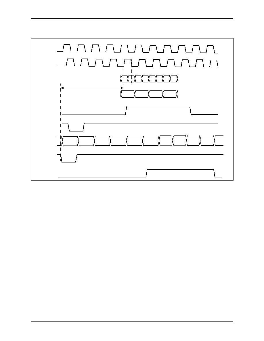
4.0 Parametric Information
Bt868/Bt869
4.2 AC Electrical Parameters
Flicker-Free Video Encoder with Ultrascale
TM
Technology
4-8
Conexant
100123B
Figure 4-3. Slave Mode with Flicker Filter Interface Timing
CLKO
CLKI
VSYNC*
(Input)
HSYNC*
(Input)
BLANK*
(Input)
BLANK*
(Output)
Internal
Sample
H_BLANK
POL POH P1L P1H P2L
PnL PnH
P0
P1
P2
Pn
Sample
H_Blank
Sample1
Sample
HCLKI
Sample
H_BLANKI
-2
Sample
H_BLANKI
Sample
H_BLANKI
-1
Counter
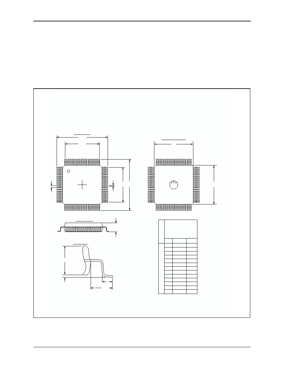
Bt868/Bt869
4.0 Parametric Information
Flicker-Free Video Encoder with Ultrascale
TM
Technology
4.3 Mechanical Drawing
100123B
Conexant
4-9
4.3 Mechanical Drawing
A detailed mechanical diagram is shown in
Figure 0-1
.
Figure 0-1. 80 MQFP Package Diagram
D
D2
E
D1
E1
E2
b
A
L
A2
A1
e
1.60
(.063)
REF.
TOP VIEW
BOTTOM VIEW
SIDE VIEW
DETAIL A
80 MQFP - 1.6/0.15mm FORM
S
Y
M
B
O
L
ALL DIMENSIONS IN
MILLIMETERS
MIN.
NOM.
MAX.
A
A1
A2
D
D1
D2
E
E1
E2
L
L1
e
b
---
0.05
16.95
16.95
0.73
0.25
---
---
2.0 REF.
---
14.0 REF.
12.35 REF.
---
14.0 REF.
12.35 REF.
0.80
16 REF.
0.65 BSC
---
2.4
0.35
17.45
17.45
1.03
0.45

4.0 Parametric Information
Bt868/Bt869
4.3 Mechanical Drawing
Flicker-Free Video Encoder with Ultrascale
TM
Technology
4-10
Conexant
100123B

100123B
Conexant
A-1
A
Appendix A. Scaling and I/O Timing
Register Calculations
The calculated values are used to program the registers controlling the total active
pixels and lines in the input frame and the output field, as well as the vertical
scaling register and the clock PLL registers. These calculations assume pixel
resolution for synchronizing the graphics controller, and master mode operation
unless otherwise stated, and require the following input values:
MFP--Minimum Front Porch Blanking in the Input in Clocks = max
(12, Controller_Minimum_Front_Porch_Blanking_Clocks);
MBP--Minimum Back Porch Blanking in the Input in Clocks = max
(4, Controller_Minimum_Back_Porch_Blanking_Clocks);
VOC--desired Vertical Overscan Compensation (e.g., 0.15)
HOC--desired Horizontal Overscan Compensation (e.g., 0.15)
V_ACTIVEI--Active Lines per Input Frame (e.g., 480 or 600)
H_ACTIVE--Active Pixels per Input Line (e.g., 640 or 800)
ALO--Target Active Lines per Output Field (See
Table A-2
)
TLO--Total Lines per Output Field (See
Table A-2
)
ATO--Active Time per Output Line (See
Table A-2
)
TTO--Total Time per Output Line (See
Table A-2
)
Table A-1
displays details of the video formats.
Table A-2
details the constant
values dependent on encoding modes.
Figures A-1
through
A-4
diagram overscan
compensation.
Tables A-3
through
A-10
display overscan values.
Table A-1. Video Formats
Mode
NTSC
NTSC-
60Hz
PAL-
BDGHI
PAL-N
PAL-Nc
PAL-M
PAL-M60Hz
PAL-60
FSC (Hz)
3,579,545
3,579,545 4,433,618.75 4,433,618.75
3,582,056.25 3,575,611.88 3,575,611.88 4,433,619.49
Burst Start
5.3
µs
5.3
µs
5.60
µs
5.60
µs
5.60
µs
5.80
µs
5.80
µs
5.60
µs
Burst End
7.82
µs
7.82
µs
7.85
µs
7.85
µs
8.11
µs
8.32
µs
8.32
µs
7.85
µs
HSYNC
Width
4.70
µs
4.70
µs
4.70
µs
4.70
µs
4.70
µs
4.70
µs
4.70
µs
4.70
µs
HSYNC
Frequency
63.555
µs
64
µs
64
µs
64
µs
64
µs
63.555
µs
64
µs
64
µs
Active Begin
9.40
µs
9.40
µs
10.5
µs
9.40
µs
10.5
µs
9.40
µs
9.40
µs
10.5
µs
Image
Center
35.667
µs 35.667 µs
36.407
µs
35.667
µs
36.407
µs
35.667
µs
35.667
µs
36.407
µs
Front Porch
1.50
µs
1.50
µs
1.50
µs
1.50
µs
1.50
µs
1.50
µs
1.50
µs
1.50
µs

Appendix A . Scaling and I/O Timing Register Calculations
Bt868/Bt869
Flicker-Free Video Encoder with Ultrascale
TM
Technology
A-2
Conexant
100123B
Table A-2. Constant Values Dependent on Encoding Mode
Modes
Interlaced
Non-Interlaced
PAL
NTSC
PAL
NTSC
ALO
288
243
288
243
TLO
312.5
262.5
312
262
ATO
52.0
µs
52.65556
µs
52.0
µs
52.65556
µs
TTO
64.0
µs
63.55556
µs
64.0
µs
63.55556
µs
Figure A-1. Overscan Compensation, 640x480 NTSC, 20 Clock Hblank
8
10
12
14
16
18
20
22
8
10
12
14
16
18
20
22
Vertical Overscan Compensation Percentage
Horizontal Overscan Compensation Percentage
Overscan Compensation Pecentage Pairs for 640x480 NTSC w/ Character Clock 1 +, 8 *, 9 o
Bt868/Bt869
Appendix A . Scaling and I/O Timing Register Calculations
Flicker-Free Video Encoder with Ultrascale
TM
Technology
100123B
Conexant
A-3
Figure A-2. Overscan Compensation, 640x480 PAL, 20 Clock Hblank
8
10
12
14
16
18
20
22
8
10
12
14
16
18
20
22
24
Vertical Overscan Compensation Percentage
Horizontal Overscan Compensation Percentage
Overscan Compensation Pecentage Pairs for 640x480 PAL w/ Character Clock 1 +, 8 *, 9 o

Appendix A . Scaling and I/O Timing Register Calculations
Bt868/Bt869
Flicker-Free Video Encoder with Ultrascale
TM
Technology
A-4
Conexant
100123B
Figure A-3. Overscan Compensation, 800x600 NTSC
8
10
12
14
16
18
20
22
8
10
12
14
16
18
20
22
24
Vertical Overscan Compensation Percentage
Horizontal Overscan Compensation Percentage
Overscan Compensation Percentage Pairs for 800x600 NTSC w/ Character Clock 1 +, 8 *, 9 o
0 us Horizontal Blanking
1 us
2 us
3 us
.75 us

Bt868/Bt869
Appendix A . Scaling and I/O Timing Register Calculations
Flicker-Free Video Encoder with Ultrascale
TM
Technology
100123B
Conexant
A-5
Figure A-4. Overscan Compensation, 800x600 PAL
8
10
12
14
16
18
20
22
8
10
12
14
16
18
20
22
Vertical Overscan Compensation Percentage
Horizontal Overscan Compensation Percentage
Overscan Compensation Pecentage Pairs for 800x600 PAL w/ Character Clock 1 +, 8 *, 9 o
Table A-3. Overscan Values, 640x480 NTSC, 1 Pixel Resolution, 2.5
Ps Hblank (1 of 3)
Controller Pixels
Encoder Pixels
Overscan (Percent)
Total
Active
Total
H_CLKI
V_LINESI
V_ACTIVEO
H_CLKO
H
V
Delta
780
665
190
988
21.81
21.81
0.00
780
595
212
884
12.61
12.76
≠0.14
784
600
210
896
13.79
13.58
0.21
780
630
200
936
17.47
17.70
≠0.23
777
575
220
851
9.23
9.47
≠0.24
785
630
200
942
18.00
17.70
0.30
777
625
202
925
16.49
16.87
≠0.38
777
650
194
962
19.70
20.16
≠0.46
775
588
215
868
11.00
11.52
≠0.52
775
651
194
961
19.62
20.16
≠0.55

Appendix A . Scaling and I/O Timing Register Calculations
Bt868/Bt869
Flicker-Free Video Encoder with Ultrascale
TM
Technology
A-6
Conexant
100123B
777
600
210
888
13.01
13.58
≠0.57
775
609
207
899
14.07
14.81
≠0.74
775
630
200
930
16.94
17.70
≠0.76
790
630
200
948
18.51
17.70
0.82
791
600
210
904
14.55
13.58
0.97
770
645
196
946
18.34
19.34
≠1.00
770
585
216
858
9.97
11.11
≠1.14
770
660
191
968
20.20
21.40
≠1.20
770
615
205
902
14.36
15.64
≠1.28
770
630
200
924
16.40
17.70
≠1.30
795
630
200
954
19.03
17.70
1.33
770
600
210
880
12.22
13.58
≠1.36
795
595
212
901
14.26
12.76
1.51
765
665
190
969
20.28
21.81
≠1.53
798
650
194
988
21.81
20.16
1.65
798
600
210
912
15.30
13.58
1.72
798
625
202
950
18.69
16.87
1.81
800
630
200
960
19.53
17.70
1.84
765
630
200
918
15.85
17.70
≠1.84
765
595
212
867
10.90
12.76
≠1.86
800
609
207
928
16.76
14.81
1.94
798
575
220
874
11.62
9.47
2.15
763
600
210
872
11.41
13.58
≠2.17
800
588
215
896
13.79
11.52
2.26
805
630
200
966
20.03
17.70
2.34
760
630
200
912
15.30
17.70
≠2.40
805
615
205
943
18.08
15.64
2.44
805
600
210
920
16.03
13.58
2.45
805
645
196
989
21.89
19.34
2.55
756
650
194
936
17.47
20.16
≠2.69
Table A-3. Overscan Values, 640x480 NTSC, 1 Pixel Resolution, 2.5
Ps Hblank (2 of 3)
Controller Pixels
Encoder Pixels
Overscan (Percent)
Total
Active
Total
H_CLKI
V_LINESI
V_ACTIVEO
H_CLKO
H
V
Delta

Bt868/Bt869
Appendix A . Scaling and I/O Timing Register Calculations
Flicker-Free Video Encoder with Ultrascale
TM
Technology
100123B
Conexant
A-7
756
625
202
900
14.17
16.87
≠2.70
805
585
216
897
13.88
11.11
2.77
810
630
200
972
20.53
17.70
2.83
755
630
200
906
14.74
17.70
≠2.96
805
570
222
874
11.62
8.64
2.97
756
600
210
864
10.59
13.58
≠2.99
Table A-3. Overscan Values, 640x480 NTSC, 1 Pixel Resolution, 2.5
Ps Hblank (3 of 3)
Controller Pixels
Encoder Pixels
Overscan (Percent)
Total
Active
Total
H_CLKI
V_LINESI
V_ACTIVEO
H_CLKO
H
V
Delta
Table A-4. Overscan Values, 640x480 NTSC, 8 Pixel Resolution, 2.5
Ps Hblank
Controller Pixels
Encoder Pixels
Overscan (Percent)
Total
Active
Total
H_CLKI
V_LINESI
V_ACTIVEO
H_CLKO
H
V
Delta
784
600
210
896
13.79
13.58
0.21
800
630
200
960
19.53
17.70
1.84
800
609
207
928
16.76
14.81
1.94
800
588
215
896
13.79
11.52
2.26
760
630
200
912
15.30
17.70
≠2.40
840
615
205
984
21.50
15.64
5.86
840
600
210
960
19.53
13.58
5.95
840
610
207
976
20.85
14.81
6.04
840
595
212
952
18.86
12.76
6.10
840
605
209
968
20.20
13.99
6.21
840
590
214
944
18.17
11.93
6.23
840
585
216
936
17.47
11.11
6.36
840
580
218
928
16.76
10.29
6.47
720
665
190
912
15.30
21.81
≠6.51
840
575
220
920
16.03
9.47
6.57
840
570
222
912
15.30
8.64
6.66
720
630
200
864
10.59
17.70
≠7.10

Appendix A . Scaling and I/O Timing Register Calculations
Bt868/Bt869
Flicker-Free Video Encoder with Ultrascale
TM
Technology
A-8
Conexant
100123B
Table A-5. Overscan Values, 640x480 NTSC, 9 Pixel Resolution, 2.5
Ps Hblank
Controller Pixels
Encoder Pixels
Overscan (Percent)
Total
Active
Total
H
V
V
H
H
V
Delta
765
665
190
969
20.28
21.81
≠1.53
765
630
200
918
15.85
17.70
≠1.84
765
595
212
867
10.90
12.76
≠1.86
756
650
194
936
17.47
20.16
≠2.69
756
625
202
900
14.17
16.87
≠2.70
810
630
200
972
20.53
17.70
2.83
756
600
210
864
10.59
13.58
≠2.99
810
595
212
918
15.85
12.76
3.09
819
600
210
936
17.47
13.58
3.89
819
625
202
975
20.77
16.87
3.90
819
575
220
897
13.88
9.47
4.42
720
665
190
912
15.30
21.81
≠6.51
720
630
200
864
10.59
17.70
≠7.10
855
595
212
969
20.28
12.76
7.52
693
650
194
858
9.97
20.16
≠10.20
882
575
220
966
20.03
9.47
10.57
900
574
220
984
21.50
9.47
12.03
675
665
190
855
9.65
21.81
≠12.16
Table A-6. Overscan Values, 640x480 PAL, 1 Pixel Resolution, 2.5
Ps Hblank (1 of 4)
Controller Pixels
Encoder Pixels
Overscan (Percent)
Total
Active
Total
H
V
V
H
H
V
Delta
945
625
240
945
16.65
16.67
≠0.02
946
625
240
946
16.73
16.67
0.07
944
625
240
944
16.56
16.67
≠0.11
947
625
240
947
16.82
16.67
0.16
943
625
240
943
16.47
16.67
≠0.20
948
625
240
948
16.91
16.67
0.24
942
625
240
942
16.38
16.67
≠0.29
949
625
240
949
17.00
16.67
0.33

Bt868/Bt869
Appendix A . Scaling and I/O Timing Register Calculations
Flicker-Free Video Encoder with Ultrascale
TM
Technology
100123B
Conexant
A-9
941
625
240
941
16.29
16.67
≠0.37
950
625
240
950
17.09
16.67
0.42
950
600
250
912
13.63
13.19
0.44
940
625
240
940
16.20
16.67
≠0.46
950
650
231
988
20.27
19.79
0.48
950
575
261
874
9.88
9.38
0.50
951
625
240
951
17.17
16.67
0.51
939
625
240
939
16.11
16.67
≠0.55
952
625
240
952
17.26
16.67
0.59
938
625
240
938
16.02
16.67
≠0.64
953
625
240
953
17.35
16.67
0.68
937
625
240
937
15.93
16.67
≠0.73
954
625
240
954
17.43
16.67
0.77
936
625
240
936
15.84
16.67
≠0.82
955
625
240
955
17.52
16.67
0.85
935
625
240
935
15.75
16.67
≠0.91
956
625
240
956
17.61
16.67
0.94
934
625
240
934
15.66
16.67
≠1.00
957
625
240
957
17.69
16.67
1.02
933
625
240
933
15.57
16.67
≠1.09
958
625
240
958
17.78
16.67
1.11
932
625
240
932
15.48
16.67
≠1.18
959
625
240
959
17.86
16.67
1.20
931
625
240
931
15.39
16.67
≠1.27
960
625
240
960
17.95
16.67
1.28
930
625
240
930
15.30
16.67
≠1.36
961
625
240
961
18.03
16.67
1.37
962
625
240
962
18.12
16.67
1.45
929
625
240
929
15.21
16.67
≠1.46
963
625
240
963
18.20
16.67
1.54
928
625
240
928
15.12
16.67
≠1.55
964
625
240
964
18.29
16.67
1.62
Table A-6. Overscan Values, 640x480 PAL, 1 Pixel Resolution, 2.5
Ps Hblank (2 of 4)
Controller Pixels
Encoder Pixels
Overscan (Percent)
Total
Active
Total
H
V
V
H
H
V
Delta

Appendix A . Scaling and I/O Timing Register Calculations
Bt868/Bt869
Flicker-Free Video Encoder with Ultrascale
TM
Technology
A-10
Conexant
100123B
927
625
240
927
15.03
16.67
≠1.64
925
650
231
962
18.12
19.79
≠1.67
965
625
240
965
18.37
16.67
1.71
926
625
240
926
14.94
16.67
≠1.73
966
625
240
966
18.46
16.67
1.79
925
625
240
925
14.84
16.67
≠1.82
967
625
240
967
18.54
16.67
1.88
925
600
250
888
11.30
13.19
≠1.90
924
625
240
924
14.75
16.67
≠1.91
968
625
240
968
18.63
16.67
1.96
923
625
240
923
14.66
16.67
≠2.01
969
625
240
969
18.71
16.67
2.04
922
625
240
922
14.57
16.67
≠2.10
970
625
240
970
18.79
16.67
2.13
921
625
240
921
14.47
16.67
≠2.19
971
625
240
971
18.88
16.67
2.21
920
625
240
920
14.38
16.67
≠2.29
972
625
240
972
18.96
16.67
2.30
973
625
240
973
19.04
16.67
2.38
919
625
240
919
14.29
16.67
≠2.38
974
625
240
974
19.13
16.67
2.46
918
625
240
918
14.19
16.67
≠2.47
975
625
240
975
19.21
16.67
2.54
917
625
240
917
14.10
16.67
≠2.57
976
625
240
976
19.29
16.67
2.63
975
600
250
936
15.84
13.19
2.65
916
625
240
916
14.01
16.67
≠2.66
977
625
240
977
19.38
16.67
2.71
915
625
240
915
13.91
16.67
≠2.75
Table A-6. Overscan Values, 640x480 PAL, 1 Pixel Resolution, 2.5
Ps Hblank (3 of 4)
Controller Pixels
Encoder Pixels
Overscan (Percent)
Total
Active
Total
H
V
V
H
H
V
Delta

Bt868/Bt869
Appendix A . Scaling and I/O Timing Register Calculations
Flicker-Free Video Encoder with Ultrascale
TM
Technology
100123B
Conexant
A-11
978
625
240
978
19.46
16.67
2.79
975
575
261
897
12.19
9.38
2.81
914
625
240
914
13.82
16.67
≠2.85
979
625
240
979
19.54
16.67
2.87
913
625
240
913
13.72
16.67
≠2.94
980
625
240
980
19.62
16.67
2.96
Table A-6. Overscan Values, 640x480 PAL, 1 Pixel Resolution, 2.5
Ps Hblank (4 of 4)
Controller Pixels
Encoder Pixels
Overscan (Percent)
Total
Active
Total
H
V
V
H
H
V
Delta
Table A-7. Overscan Values, 640x480 PAL, 8 Pixel Resolution, 2.5
Ps Hblank (1 of 2)
Controller Pixels
Encoder Pixels
Overscan (Percent)
Total
Active
Total
H
V
V
H
H
V
Delta
944
625
240
944
16.56
16.67
≠0.11
952
625
240
952
17.26
16.67
0.59
936
625
240
936
15.84
16.67
≠0.82
960
625
240
960
17.95
16.67
1.28
928
625
240
928
15.12
16.67
≠1.55
968
625
240
968
18.63
16.67
1.96
920
625
240
920
14.38
16.67
≠2.29
976
625
240
976
19.29
16.67
2.63
912
625
240
912
13.63
16.67
≠3.04
984
625
240
984
19.95
16.67
3.28
904
625
240
904
12.87
16.67
≠3.80
992
625
240
992
20.60
16.67
3.93
1000
625
240
1000
21.23
16.67
4.56
896
625
240
896
12.09
16.67
≠4.58
1000
620
242
992
20.60
15.97
4.62
1000
615
244
984
19.95
15.28
4.67
1000
610
246
976
19.29
14.58
4.71
1000
605
248
968
18.63
13.89
4.74
1000
600
250
960
17.95
13.19
4.75
1000
630
239
1008
21.86
17.01
4.84
1000
575
261
920
14.38
9.38
5.01

Appendix A . Scaling and I/O Timing Register Calculations
Bt868/Bt869
Flicker-Free Video Encoder with Ultrascale
TM
Technology
A-12
Conexant
100123B
1000
580
259
928
15.12
10.07
5.05
1000
585
257
936
15.84
10.76
5.08
1000
590
255
944
16.56
11.46
5.10
1000
595
253
952
17.26
12.15
5.11
1008
625
240
1008
21.86
16.67
5.19
888
625
240
888
11.30
16.67
≠5.37
880
625
240
880
10.49
16.67
≠6.18
872
625
240
872
9.67
16.67
≠7.00
Table A-7. Overscan Values, 640x480 PAL, 8 Pixel Resolution, 2.5
Ps Hblank (2 of 2)
Controller Pixels
Encoder Pixels
Overscan (Percent)
Total
Active
Total
H
V
V
H
H
V
Delta
Table A-8. Overscan Values, 640x480 PAL, 9 Pixel Resolution, 2.5
Ps Hblank
Controller Pixels
Encoder Pixels
Overscan (Percent)
Total
Active
Total
H
V
V
H
H
V
Delta
945
625
240
945
16.65
16.67
≠0.02
954
625
240
954
17.43
16.67
0.77
936
625
240
936
15.84
16.67
≠0.82
963
625
240
963
18.20
16.67
1.54
927
625
240
927
15.03
16.67
≠1.64
972
625
240
972
18.96
16.67
2.30
918
625
240
918
14.19
16.67
≠2.47
981
625
240
981
19.71
16.67
3.04
909
625
240
909
13.35
16.67
≠3.32
990
625
240
990
20.44
16.67
3.77
900
650
231
936
15.84
19.79
≠3.95
900
625
240
900
12.48
16.67
≠4.19
999
625
240
999
21.15
16.67
4.49
891
625
240
891
11.59
16.67
≠5.07
1008
625
240
1008
21.86
16.67
5.19
882
625
240
882
10.69
16.67
≠5.97
873
625
240
873
9.77
16.67
≠6.89

Bt868/Bt869
Appendix A . Scaling and I/O Timing Register Calculations
Flicker-Free Video Encoder with Ultrascale
TM
Technology
100123B
Conexant
A-13
Table A-9. Overscan Values, 800x600 NTSC (1 of 5)
Controller Pixels
Encoder Pixels
Overscan (Percent)
Hblank and Character Clock
Resolution
Total
Active
Total
H
V
V
H
H
V
Delta
Hblank
Resol
800
777
203
1184
18.45
16.46
1.98
0.00
1
800
819
193
1248
22.63
20.58
2.05
0.00
1
800
798
198
1216
20.59
18.52
2.07
0.00
1
800
756
209
1152
16.18
13.99
2.19
0.00
1
800
714
221
1088
11.25
9.05
2.20
0.00
1
800
735
215
1120
13.79
11.52
2.26
0.00
1
805
825
191
1265
23.67
21.40
2.27
0.13
1
805
780
202
1196
19.26
16.87
2.39
0.13
1
805
750
210
1150
16.03
13.58
2.45
0.14
1
805
765
206
1173
17.68
15.23
2.45
0.14
1
805
810
195
1242
22.25
19.75
2.50
0.13
1
805
720
219
1104
12.54
9.88
2.66
0.14
1
805
795
199
1219
20.79
18.11
2.68
0.13
1
805
735
215
1127
14.32
11.52
2.80
0.14
1
810
805
196
1242
22.25
19.34
2.91
0.26
1
810
770
205
1188
18.72
15.64
3.08
0.27
1
812
750
210
1160
16.76
13.58
3.18
0.33
1
810
735
215
1134
14.85
11.52
3.33
0.28
1
819
800
197
1248
22.63
18.93
3.70
0.48
1
815
735
215
1141
15.37
11.52
3.85
0.42
1
819
750
210
1170
17.47
13.58
3.89
0.52
1
819
775
204
1209
20.13
16.05
4.08
0.50
1
825
805
196
1265
23.67
19.34
4.33
0.63
1
819
725
218
1131
14.62
10.29
4.34
0.53
1
825
784
201
1232
21.62
17.28
4.34
0.64
1
820
735
215
1148
15.89
11.52
4.37
0.55
1
825
777
203
1221
20.92
16.46
4.46
0.65
1
825
798
198
1254
23.00
18.52
4.48
0.63
1
825
770
205
1210
20.20
15.64
4.56
0.66
1
826
750
210
1180
18.17
13.58
4.59
0.70
1
825
791
200
1243
22.32
17.70
4.62
0.64
1
825
763
207
1199
19.47
14.81
4.65
0.66
1

Appendix A . Scaling and I/O Timing Register Calculations
Bt868/Bt869
Flicker-Free Video Encoder with Ultrascale
TM
Technology
A-14
Conexant
100123B
825
756
209
1188
18.72
13.99
4.73
0.67
1
825
749
211
1177
17.96
13.17
4.79
0.67
1
825
742
213
1166
17.19
12.35
4.84
0.68
1
825
735
215
1155
16.40
11.52
4.88
0.69
1
825
714
221
1122
13.94
9.05
4.89
0.71
1
825
728
217
1144
15.59
10.70
4.89
0.69
1
825
721
219
1133
14.77
9.88
4.90
0.70
1
833
750
210
1190
18.86
13.58
5.28
0.88
1
830
735
215
1162
16.90
11.52
5.38
0.82
1
840
780
202
1248
22.63
16.87
5.76
1.02
1
840
785
201
1256
23.12
17.28
5.84
1.01
1
835
735
215
1169
17.40
11.52
5.88
0.95
1
840
765
206
1224
21.11
15.23
5.88
1.04
1
840
790
200
1264
23.61
17.70
5.91
1.01
1
840
750
210
1200
19.53
13.58
5.95
1.06
1
840
770
205
1232
21.62
15.64
5.99
1.03
1
840
755
209
1208
20.07
13.99
6.07
1.05
1
840
775
204
1240
22.13
16.05
6.08
1.03
1
840
740
213
1184
18.45
12.35
6.10
1.07
1
840
760
208
1216
20.59
14.40
6.19
1.05
1
840
730
216
1168
17.33
11.11
6.22
1.09
1
840
745
212
1192
18.99
12.76
6.24
1.07
1
840
720
219
1152
16.18
9.88
6.30
1.10
1
840
735
215
1176
17.89
11.52
6.37
1.08
1
840
725
218
1160
16.76
10.29
6.47
1.10
1
840
715
221
1144
15.59
9.05
6.54
1.11
1
847
750
210
1210
20.20
13.58
6.62
1.23
1
850
777
203
1258
23.24
16.46
6.78
1.26
1
845
735
215
1183
18.38
11.52
6.85
1.21
1
850
756
209
1224
21.11
13.99
7.12
1.30
1
854
750
210
1220
20.85
13.58
7.27
1.41
1
850
735
215
1190
18.86
11.52
7.33
1.34
1
Table A-9. Overscan Values, 800x600 NTSC (2 of 5)
Controller Pixels
Encoder Pixels
Overscan (Percent)
Hblank and Character Clock
Resolution
Total
Active
Total
H
V
V
H
H
V
Delta
Hblank
Resol

Bt868/Bt869
Appendix A . Scaling and I/O Timing Register Calculations
Flicker-Free Video Encoder with Ultrascale
TM
Technology
100123B
Conexant
A-15
855
770
205
1254
23.00
15.64
7.36
1.39
1
850
714
221
1156
16.47
9.05
7.42
1.37
1
855
735
215
1197
19.33
11.52
7.81
1.46
1
861
750
210
1230
21.50
13.58
7.92
1.58
1
861
775
204
1271
24.03
16.05
7.98
1.53
1
860
735
215
1204
19.80
11.52
8.28
1.58
1
861
725
218
1189
18.79
10.29
8.50
1.63
1
868
750
210
1240
22.13
13.58
8.55
1.74
1
865
735
215
1211
20.26
11.52
8.74
1.71
1
875
762
207
1270
23.97
14.81
9.15
1.88
1
875
750
210
1250
22.75
13.58
9.17
1.91
1
870
735
215
1218
20.72
11.52
9.20
1.83
1
875
759
208
1265
23.67
14.40
9.26
1.88
1
875
747
211
1245
22.44
13.17
9.27
1.91
1
875
744
212
1240
22.13
12.76
9.37
1.92
1
875
756
209
1260
23.36
13.99
9.37
1.89
1
875
741
213
1235
21.81
12.35
9.47
1.93
1
875
753
210
1255
23.06
13.58
9.48
1.90
1
875
726
217
1210
20.20
10.70
9.50
1.97
1
875
738
214
1230
21.50
11.93
9.56
1.94
1
875
723
218
1205
19.87
10.29
9.58
1.98
1
875
735
215
1225
21.18
11.52
9.65
1.95
1
875
720
219
1200
19.53
9.88
9.66
1.99
1
875
717
220
1195
19.20
9.47
9.73
1.99
1
875
732
216
1220
20.85
11.11
9.74
1.95
1
882
750
210
1260
23.36
13.58
9.78
2.07
1
875
714
221
1190
18.86
9.05
9.80
2.00
1
875
729
217
1215
20.53
10.70
9.83
1.96
1
880
735
215
1232
21.62
11.52
10.10
2.06
1
889
750
210
1270
23.97
13.58
10.39
2.23
1
882
725
218
1218
20.72
10.29
10.43
2.14
1
885
735
215
1239
22.07
11.52
10.54
2.18
1
Table A-9. Overscan Values, 800x600 NTSC (3 of 5)
Controller Pixels
Encoder Pixels
Overscan (Percent)
Hblank and Character Clock
Resolution
Total
Active
Total
H
V
V
H
H
V
Delta
Hblank
Resol

Appendix A . Scaling and I/O Timing Register Calculations
Bt868/Bt869
Flicker-Free Video Encoder with Ultrascale
TM
Technology
A-16
Conexant
100123B
890
735
215
1246
22.50
11.52
10.98
2.30
1
895
735
215
1253
22.94
11.52
11.41
2.41
1
900
735
215
1260
23.36
11.52
11.84
2.52
1
900
728
217
1248
22.63
10.70
11.93
2.55
1
900
721
219
1236
21.88
9.88
12.00
2.57
1
900
714
221
1224
21.11
9.05
12.06
2.60
1
905
735
215
1267
23.79
11.52
12.27
2.63
1
903
725
218
1247
22.57
10.29
12.28
2.62
1
910
720
219
1248
22.63
9.88
12.75
2.80
1
925
714
221
1258
23.24
9.05
14.19
3.16
1
800
777
203
1184
18.45
16.46
1.98
0.00
8
800
819
193
1248
22.63
20.58
2.05
0.00
8
800
798
198
1216
20.59
18.52
2.07
0.00
8
800
756
209
1152
16.18
13.99
2.19
0.00
8
800
714
221
1088
11.25
9.05
2.20
0.00
8
800
735
215
1120
13.79
11.52
2.26
0.00
8
840
780
202
1248
22.63
16.87
5.76
1.02
8
840
785
201
1256
23.12
17.28
5.84
1.01
8
840
765
206
1224
21.11
15.23
5.88
1.04
8
840
790
200
1264
23.61
17.70
5.91
1.01
8
840
750
210
1200
19.53
13.58
5.95
1.06
8
840
770
205
1232
21.62
15.64
5.99
1.03
8
840
755
209
1208
20.07
13.99
6.07
1.05
8
840
775
204
1240
22.13
16.05
6.08
1.03
8
840
740
213
1184
18.45
12.35
6.10
1.07
8
840
760
208
1216
20.59
14.40
6.19
1.05
8
840
730
216
1168
17.33
11.11
6.22
1.09
8
840
745
212
1192
18.99
12.76
6.24
1.07
8
840
720
219
1152
16.18
9.88
6.30
1.10
8
840
735
215
1176
17.89
11.52
6.37
1.08
8
840
725
218
1160
16.76
10.29
6.47
1.10
8
840
715
221
1144
15.59
9.05
6.54
1.11
8
Table A-9. Overscan Values, 800x600 NTSC (4 of 5)
Controller Pixels
Encoder Pixels
Overscan (Percent)
Hblank and Character Clock
Resolution
Total
Active
Total
H
V
V
H
H
V
Delta
Hblank
Resol

Bt868/Bt869
Appendix A . Scaling and I/O Timing Register Calculations
Flicker-Free Video Encoder with Ultrascale
TM
Technology
100123B
Conexant
A-17
880
735
215
1232
21.62
11.52
10.10
2.06
8
810
805
196
1242
22.25
19.34
2.91
0.26
9
810
770
205
1188
18.72
15.64
3.08
0.27
9
810
735
215
1134
14.85
11.52
3.33
0.28
9
819
800
197
1248
22.63
18.93
3.70
0.48
9
819
750
210
1170
17.47
13.58
3.89
0.52
9
819
775
204
1209
20.13
16.05
4.08
0.50
9
819
725
218
1131
14.62
10.29
4.34
0.53
9
855
770
205
1254
23.00
15.64
7.36
1.39
9
855
735
215
1197
19.33
11.52
7.81
1.46
9
882
750
210
1260
23.36
13.58
9.78
2.07
9
882
725
218
1218
20.72
10.29
10.43
2.14
9
900
735
215
1260
23.36
11.52
11.84
2.52
9
900
728
217
1248
22.63
10.70
11.93
2.55
9
900
721
219
1236
21.88
9.88
12.00
2.57
9
900
714
221
1224
21.11
9.05
12.06
2.60
9
Table A-9. Overscan Values, 800x600 NTSC (5 of 5)
Controller Pixels
Encoder Pixels
Overscan (Percent)
Hblank and Character Clock
Resolution
Total
Active
Total
H
V
V
H
H
V
Delta
Hblank
Resol
Table A-10. Overscan Values, 800x600, PAL, > 2.5
Ps Hblank (1 of 3)
Controller Pixels
Encoder Pixels
Overscan (Percent)
Character
Clock
Total
Active
Total
H
V
V
H
H
V
Delta
Resol
945
750
250
1134
13.17
13.19
≠0.02
1
950
750
250
1140
13.63
13.19
0.44
1
950
775
242
1178
16.42
15.97
0.44
1
940
750
250
1128
12.71
13.19
≠0.48
1
950
725
259
1102
10.65
10.07
0.58
1
950
800
235
1216
19.03
18.40
0.63
1
950
825
228
1254
21.48
20.83
0.65
1
955
750
250
1146
14.08
13.19
0.89
1
935
750
250
1122
12.24
13.19
≠0.95
1
960
750
250
1152
14.53
13.19
1.34
1
930
750
250
1116
11.77
13.19
≠1.42
1

Appendix A . Scaling and I/O Timing Register Calculations
Bt868/Bt869
Flicker-Free Video Encoder with Ultrascale
TM
Technology
A-18
Conexant
100123B
925
825
228
1221
19.36
20.83
≠1.47
1
925
800
235
1184
16.84
18.40
≠1.56
1
965
750
250
1158
14.97
13.19
1.78
1
925
775
242
1147
14.16
15.97
≠1.81
1
925
750
250
1110
11.30
13.19
≠1.90
1
970
750
250
1164
15.41
13.19
2.22
1
920
750
250
1104
10.81
13.19
≠2.38
1
975
775
242
1209
18.56
15.97
2.59
1
975
750
250
1170
15.84
13.19
2.65
1
975
800
235
1248
21.10
18.40
2.70
1
915
750
250
1098
10.33
13.19
≠2.87
1
975
725
259
1131
12.94
10.07
2.87
1
980
750
250
1176
16.27
13.19
3.08
1
910
750
250
1092
9.83
13.19
≠3.36
1
985
750
250
1182
16.70
13.19
3.50
1
900
825
228
1188
17.12
20.83
≠3.71
1
905
750
250
1086
9.34
13.19
≠3.86
1
900
800
235
1152
14.53
18.40
≠3.87
1
990
750
250
1188
17.12
13.19
3.93
1
900
775
242
1116
11.77
15.97
≠4.20
1
995
750
250
1194
17.54
13.19
4.34
1
1000
785
239
1256
21.61
17.01
4.59
1
1000
775
242
1240
20.60
15.97
4.62
1
1000
750
250
1200
17.95
13.19
4.75
1
1000
780
241
1248
21.10
16.32
4.79
1
1000
760
247
1216
19.03
14.24
4.79
1
1000
770
244
1232
20.08
15.28
4.80
1
1000
745
252
1192
17.40
12.50
4.90
1
1000
730
257
1168
15.70
10.76
4.94
1
1000
755
249
1208
18.49
13.54
4.95
1
1000
765
246
1224
19.56
14.58
4.97
1
960
750
250
1152
14.53
13.19
1.34
8
Table A-10. Overscan Values, 800x600, PAL, > 2.5
Ps Hblank (2 of 3)
Controller Pixels
Encoder Pixels
Overscan (Percent)
Character
Clock
Total
Active
Total
H
V
V
H
H
V
Delta
Resol

Bt868/Bt869
Appendix A . Scaling and I/O Timing Register Calculations
Flicker-Free Video Encoder with Ultrascale
TM
Technology
100123B
Conexant
A-19
920
750
250
1104
10.81
13.19
≠2.38
8
1000
785
239
1256
21.61
17.01
4.59
8
1000
775
242
1240
20.60
15.97
4.62
8
1000
750
250
1200
17.95
13.19
4.75
8
1000
780
241
1248
21.10
16.32
4.79
8
1000
760
247
1216
19.03
14.24
4.79
8
1000
770
244
1232
20.08
15.28
4.80
8
1000
745
252
1192
17.40
12.50
4.90
8
1000
730
257
1168
15.70
10.76
4.94
8
1000
755
249
1208
18.49
13.54
4.95
8
1000
765
246
1224
19.56
14.58
4.97
8
1000
740
254
1184
16.84
11.81
5.03
8
1000
725
259
1160
15.12
10.07
5.05
8
1000
720
261
1152
14.53
9.38
5.15
8
1000
735
256
1176
16.27
11.11
5.16
8
1000
715
263
1144
13.93
8.68
5.25
8
1040
750
250
1248
21.10
13.19
7.91
8
945
750
250
1134
13.17
13.19
≠0.02
9
900
825
228
1188
17.12
20.83
≠3.71
9
900
800
235
1152
14.53
18.40
≠3.87
9
990
750
250
1188
17.12
13.19
3.93
9
900
775
242
1116
11.77
15.97
≠4.20
9
1035
750
250
1242
20.72
13.19
7.53
9
Table A-10. Overscan Values, 800x600, PAL, > 2.5
Ps Hblank (3 of 3)
Controller Pixels
Encoder Pixels
Overscan (Percent)
Character
Clock
Total
Active
Total
H
V
V
H
H
V
Delta
Resol

Appendix A . Scaling and I/O Timing Register Calculations
Bt868/Bt869
Flicker-Free Video Encoder with Ultrascale
TM
Technology
A-20
Conexant
100123B

100123B
Conexant
B-1
B
Appendix B. Approved Crystal
Vendors
Conexant conducted a series of internal tests and used the results to generate this
list of approved crystal vendors. Contact your local Conexant Field Applications
Engineer for additional details.
Standard Crystal (El Monte, CA)
Phone Number:
(626)443-2121
FAX Number:
(626)443-9049
E-mail:
stdxtl@worldnet.att.net
Part Numbers for 13.500 MHz, Fundamental, 20pF Load Crystal with an HC49U Type of Package:
Full Height/50 ppm Total Tolerance:
AAK13M500000GXE20A
Half-Height/50 ppm:
AAL13M500000GXE20A
Full Height/25 ppm:
Did Not Qualify
MMD Components (Irvine, CA)
Phone Number:
(949)753-5888
FAX Number:
(949)753-5889
E-mail:
mmdcomp@earthlink.net
Part Numbers for 13.500 MHz, Fundamental, 20pF Load Crystal with an HC49U Type of Package:
Full Height/50ppm Total Tolerance:
A20BA1-13.500 MHz.
Half-Height/50 ppm:
B20BA1-13,500 MHz
Full Height/25 ppm:
Did Not Qualify
General Electronics (San Marcos, CA)
Phone Number:
(760)591-4170
FAX Number:
(760)591-4164
E-mail:
gedlm@4dcomm.com
Part Numbers for 13.500 MHz, Fundamental, 20pF Load Crystal with an HC49U Type of Package:
Full Height/50 ppm Total Tolerance:
PKHC49/U-13.500-.020-.005
Half-Height/50 ppm:
PKHC49/US-13.500-.020-.005
Full Height/25 ppm:
PKHC49/U-13.500-.0025-15R
Fox Electronics (Fort Myers, FL)
Phone Number:
(941)693-0099
FAX Number:
(941)693-1554
E-mail:
barbc@foxonline.com
Part Numbers for 13.500 MHz, Fundamental, 20pF Load Crystal with an HC49U Type of Package:
Full Height/50 ppm Total Tolerance:
HC49U-13.500 MHz-/50/0/70/20 pF
Half Height/50 ppm:
HC49S 13.500-/50/0/70/20 pF
Full Height/25 ppm:
HC49U 13.500-/25/0/70/20 pF

Appendix B . Approved Crystal Vendors
Bt868/Bt869
Flicker-Free Video Encoder with Ultrascale
TM
Technology
B-2
Conexant
100123B
Bomar (Middlesex, NJ)
Phone Number:
(732)356-7787
FAX Number:
(732)356-7362
E-mail:
sales@bomarcrystal.com
Part Numbers for 13.500 MHz, Fundamental, 20pF Load Crystal with an HC49U Type of Package:
Full Height/50 ppm Total Tolerance:
BRC1C14F-13.50000
Half Height/50 ppm:
ACR-49S012025-13.50000
Full Height/25 ppm:
BRCIE14F-13.50000
HY-Q (Erlanger, Kentucky)
Phone Number:
(606)283-5000
FAX Number:
(606)283-0883
E-mail:
Cpainter@hyqusa.com
Part Numbers for 13.500 MHz, Fundamental, 20pF Load Crystal with an HC49U Type of Package:
Full Height/50 ppm Total Tolerance:
HT81818/01
Half Height/50 ppm:
SC30002/01
Full Height/25 ppm:
HT81819/01
ILSI America (Kirkland, WA)
Phone Number:
(425)828-4886 / (888)355-4574
FAX Number:
(425)828-4878
E-mail:
ilsiam@ilsiamerica.co
Part Numbers for 13.500 MHz, Fundamental, 20pF Load Crystal with an HC49U Type of Package:
Full Height/50 ppm Total Tolerance:
HC49U-25/25-13.500-20
Half Height/50 ppm:
HC49US-FB1F20-13.500
Full Height/25 ppm:
Did Not Qualify
Cardinal Components (Wayne, NJ)
Phone Number:
(973)785-1333
FAX Number:
(973)785-0053
E-mail:
dbabcock@cardinalxtal.com
Part Numbers for 13.500 MHz, Fundamental, 20pF Load Crystal with an HC49U Type of Package:
Full Height/50 ppm Total Tolerance:
C49-A4BRC7-25-13.5D20
Half Height/50 ppm:
CLP-A4B6C4-50-13.5D20
Full Height/25 ppm:
C49-A4B6C4-25-13.5D20
Raltron Electronics Corp. (Miami, FL)
Phone Number:
(305)593-6033
FAX Number:
(305)594-3973
E-mail:
maria@raltron.com
Part Numbers for 13.500 MHz, Fundamental, 20pF Load Crystal with an HC49U Type of Package:
Full Height/50 ppm Total Tolerance:
A-13.500-20-RS1
Half Height/50 ppm:
AS-13.500-20-RS1
Full Height/25 ppm:
A-13.500-20-RS1
Valpey-Fisher (Hopkinton, MA)
Phone Number:
(800)982-5737
FAX Number:
(508)497-6377

Bt868/Bt869
Appendix B . Approved Crystal Vendors
Flicker-Free Video Encoder with Ultrascale
TM
Technology
100123B
Conexant
B-3
E-mail:
angleassoc@aol.com
Part Numbers for 13.500 MHz, Fundamental, 20pF Load Crystal with an HC49U Type of Package:
Full Height/50 ppm Total Tolerance:
M490013.500020RSVM
Half Height/50 ppm:
M49K013.50002099VM
Full Height/25 ppm:
M490013.50002099VM
Telequarz Group (Germany)
Phone Number:
Telequarz-USA Inc. (Ft. Mill, SC): (803)547-0770
FAX Number:
(507)547-0775
E-mail:
info@telequarz.de
Part Numbers for 13.500 MHz, Fundamental, 20pF Load Crystal with an HC49U Type of Package:
Full Height/50 ppm Total Tolerance:
TQ RSD 13.5FH50
Half Height/50 ppm:
TQRSD 13.5LP50
Full Height/25 ppm:
TQ RSD 13.5FH25

Appendix B . Approved Crystal Vendors
Bt868/Bt869
Flicker-Free Video Encoder with Ultrascale
TM
Technology
B-4
Conexant
100123B


Further Information
literature@conexant.com
(800) 854-8099 (North America)
(949) 483-6996 (International)
Printed in USA
World Headquarters
Conexant Systems, Inc.
4311 Jamboree Road
Newport Beach, CA
92660-3007
Phone: (949) 483-4600
Fax 1:
(949) 483-4078
Fax 2:
(949) 483-4391
Americas
U.S. Northwest/
Pacific Northwest ≠ Santa Clara
Phone: (408) 249-9696
Fax:
(408) 249-7113
U.S. Southwest ≠ Los Angeles
Phone: (805) 376-0559
Fax:
(805) 376-8180
U.S. Southwest ≠ Orange County
Phone: (949) 483-9119
Fax:
(949) 483-9090
U.S. Southwest ≠ San Diego
Phone: (858) 713-3374
Fax:
(858) 713-4001
U.S. North Central ≠ Illinois
Phone: (630) 773-3454
Fax:
(630) 773-3907
U.S. South Central ≠ Texas
Phone: (972) 733-0723
Fax:
(972) 407-0639
U.S. Northeast ≠ Massachusetts
Phone: (978) 367-3200
Fax:
(978) 256-6868
U.S. Southeast ≠ North Carolina
Phone: (919) 858-9110
Fax:
(919) 858-8669
U.S. Southeast ≠ Florida/
South America
Phone: (727) 799-8406
Fax:
(727) 799-8306
U.S. Mid-Atlantic ≠ Pennsylvania
Phone: (215) 244-6784
Fax:
(215) 244-9292
Canada ≠ Ontario
Phone: (613) 271-2358
Fax:
(613) 271-2359
Europe
Europe Central ≠ Germany
Phone: +49 89 829-1320
Fax:
+49 89 834-2734
Europe North ≠ England
Phone: +44 1344 486444
Fax:
+44 1344 486555
Europe ≠ Israel/Greece
Phone: +972 9 9524000
Fax:
+972 9 9573732
Europe South ≠ France
Phone: +33 1 41 44 36 51
Fax:
+33 1 41 44 36 90
Europe Mediterranean ≠ Italy
Phone: +39 02 93179911
Fax:
+39 02 93179913
Europe ≠ Sweden
Phone: +46 (0) 8 5091 4319
Fax:
+46 (0) 8 590 041 10
Europe ≠ Finland
Phone: +358 (0) 9 85 666 435
Fax:
+358 (0) 9 85 666 220
Asia ≠ Pacific
Taiwan
Phone: (886-2) 2-720-0282
Fax:
(886-2) 2-757-6760
Australia
Phone: (61-2) 9869 4088
Fax:
(61-2) 9869 4077
China ≠ Central
Phone: 86-21-6361-2515
Fax:
86-21-6361-2516
China ≠ South
Phone: (852) 2 827-0181
Fax:
(852) 2 827-6488
China ≠ South (Satellite)
Phone: (86) 755-518-2495
China ≠ North
Phone: (86-10) 8529-9777
Fax:
(86-10) 8529-9778
India
Phone: (91-11) 692-4789
Fax:
(91-11) 692-4712
Korea
Phone: (82-2) 565-2880
Fax:
(82-2) 565-1440
Korea (Satellite)
Phone: (82-53) 745-2880
Fax:
(82-53) 745-1440
Singapore
Phone: (65) 737 7355
Fax:
(65) 737 9077
Japan
Phone: (81-3) 5371 1520
Fax:
(81-3) 5371 1501
www.conexant.com
0.0 Sales Offices