 | –≠–ª–µ–∫—Ç—Ä–æ–Ω–Ω—ã–π –∫–æ–º–ø–æ–Ω–µ–Ω—Ç: D355B | –°–∫–∞—á–∞—Ç—å:  PDF PDF  ZIP ZIP |

2
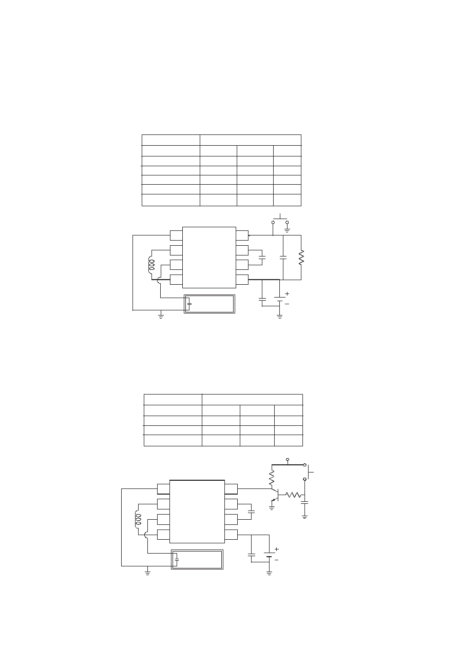
PIN # NAME
FUNCTION
Typical Output Waveform
Load B*
Physical Data
1
GND
System ground connection
2
L-
Negative input to inductor
3
Vout
High voltage AC output to lamp
4
L+
Positive input to inductor
5
V+
DC power supply input
6
CLF1
Lamp frequency capacitor/clock input
7
CLF2
Lamp frequency capacitor/clock input
8
E'
System enable; Power Down Control
Note: Please consult factory for bare die physical data
and bond pad locations
Absolute Maximum Ratings
Note: The above are stress ratings only. Functional operation of the device at these ratings or any other above those
indicated in the specifications is not implied. Exposure to absolute maximum rating conditions for extended periods of
time may affect reliability.
Parameter
Symbol
Minimum
Maximum
Unit
Comments
* Load B approximates a 5in
2
EL lamp.
Supply voltage
Operating range
V+
1.0
7.0
V
E' = GND
Withstand range
-0.5
10.0
E' = V+
Enable Voltage
E'
-0.5
(V+) +0.5
V
Output Voltage
Vout
220
Vpp
Peak to peak voltage
CLF Voltage
V
CLF
0
(V+)+0.3
V
External clock input
Operating temperature
T
a
-40
85
∞C
Storage temperature
T
s
-65
150
∞C
100
22 nF
10k
47 nF
1
2
3
4
5
6
7
8
3
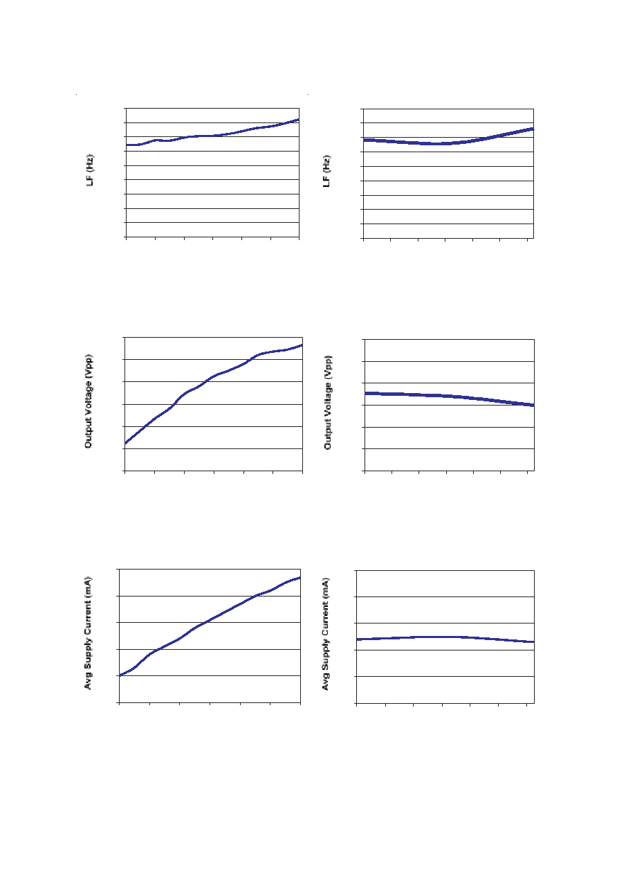
Supply Current vs. Ambient
Temperature
0
10
20
30
40
50
-40
-20
0
20
40
60
80
Temperature ( C)
Typical Performance Characteristics Using Standard Test Circuit
o
Output Frequency vs. DC Supply
Voltage
0
50
100
150
200
250
300
350
400
450
1
2
3
4
5
6
7
DC Input Voltage
Output Frequency vs. Ambient
Temperature
0
50
100
150
200
250
300
350
400
450
-40
-20
0
20
40
60
80
Temperature ( C)
Output Voltage vs. DC Supply Voltage
0
40
80
120
160
200
240
1
2
3
4
5
6
7
DC Input Voltage
Output Voltage vs. Ambient
Temperature
0
40
80
120
160
200
240
-40
-20
0
20
40
60
80
Temperature ( C)
Supply Current vs. DC Supply Voltage
0
10
20
30
40
50
1
2
3
4
5
6
7
DC Input Voltage
o
o
4
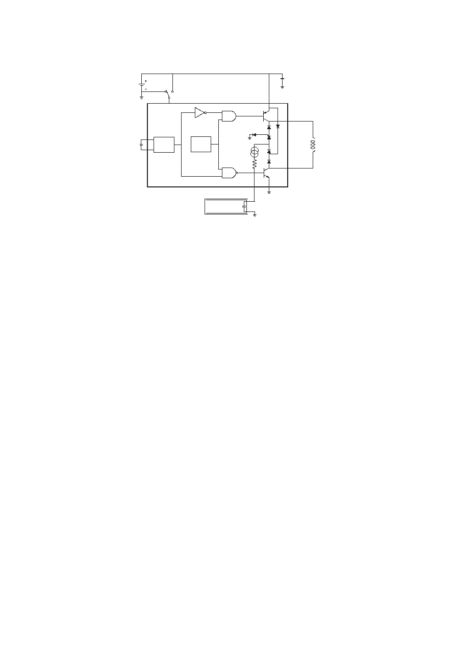
Theory of Operation
Electroluminescent (EL) lamps are essentially capacitors with one transparent electrode and a special phosphor
material in the dielectric. When a strong AC voltage is applied across the EL lamp electrodes, the phosphor
glows. The required AC voltage is typically not present in most systems and must be generated from a low
voltage DC source. Thus, Durel developed its patented Three-Port (3P) switch-mode inverter circuit to
convert the available DC supply to an optimal drive signal for high brightness and low-noise EL lamp
applications. The Durel 3P topology offers the simplicity of a single DC input, single AC output, and a
shared common ground that provides an integrated EMI shielding.
The D355B drives the EL lamp by repeatedly pumping charge through an external inductor with current
from a DC source and discharging into the capacitance of the EL lamp load. With each high frequency (HF)
cycle the voltage on the lamp is increased. At a period specified by the lamp frequency (LF) oscillator, the
voltage on the lamp is discharged to ground and the polarity of the inductive charging is reversed. By this
means, an alternating positive and negative voltage is developed at the single output lead of the device to one
of the electrodes of the EL lamp. The other lamp electrode is commonly connected to a ground plane, which
can then be considered as electrical shielding for any underlying circuitry on the application.
The EL driving system is divided into several parts: on-chip logic and control, on-chip high voltage output
circuitry, discharge logic circuitry, and off-chip components. The on-chip logic controls the output frequency
(LF), as well as the inductor switching frequency (HF), and HF and LF duty cycles. These signals are
combined and buffered to regulate the high voltage output circuitry. The output circuitry handles the power
through the inductor and delivers the high voltage to the lamp. The selection of off-chip components provides
a degree of flexibility to accommodate various lamp sizes, system voltages, and brightness levels. Since a
key objective for EL driver systems is to save space and cost, required off-chip components were kept to a
minimum.
Durel provides a D355B Designer's Kit, which includes a printed circuit evaluation board intended to aid
you in developing an EL lamp driver configuration using the D355B that meets your requirements. A section
on designing with the D355B is included in this datasheet to serve as a guide to help you select the appropriate
external components to complete your D355B EL driver system.
Typical D355B configurations for driving EL lamps in various applications are shown on the following
page. The expected system outputs, such as lamp luminance, lamp output frequency and voltage and average
supply current draw, for the various sample configurations are also shown with each respective figure.
Block Diagram of the Driver Circuitry
High
Frequency
Oscillator
Low
Frequency
Oscillator
EL Lamp
CLF1
CLF2
E'
V+
L+
L-
GND
VOUT
F
1.0
µ

5
Typical D355B EL Driver Configurations
1
2
3
4
8
7
6
5
GND
L-
VOUT
L+
E'
CLF2
CLF1
V+
1 in
2
EL Lamp
2.2 mH
Sumida
CLS62-222
1.5 V
6.8 nF
D355
OFF
ON
GND
1.5V
1.0
µ
F
1.5V Analog Watch
Typical Output
Luminance = 3.5 fL (12 cd/m
2
)
Lamp Frequency = 220 Hz
Supply Current = 10 mA
Vout = 178 Vpp
Load = 1 in
2
Durel Æ3 Green EL
1
2
3
4
8
7
6
5
GND
L-
VOUT
L+
E'
CLF2
CLF1
V+
1 in
2
EL Lamp
F
1.0
µ
4.7 mH
Coilcraft
DS1608BL-475
3.0 V
3.3 nF
D355
1M
1M
E
OFF
ON
GND
3.0V
MMBTA06
3.0 V Handset LCD or Digital Watch
Typical Output
Luminance = 8.6 fL (29.5 cd/m
2
)
Lamp Frequency = 475 Hz
Supply Current = 14 mA
Vout = 208 Vpp
Load = 1 in
2
Durel Æ3 Green EL
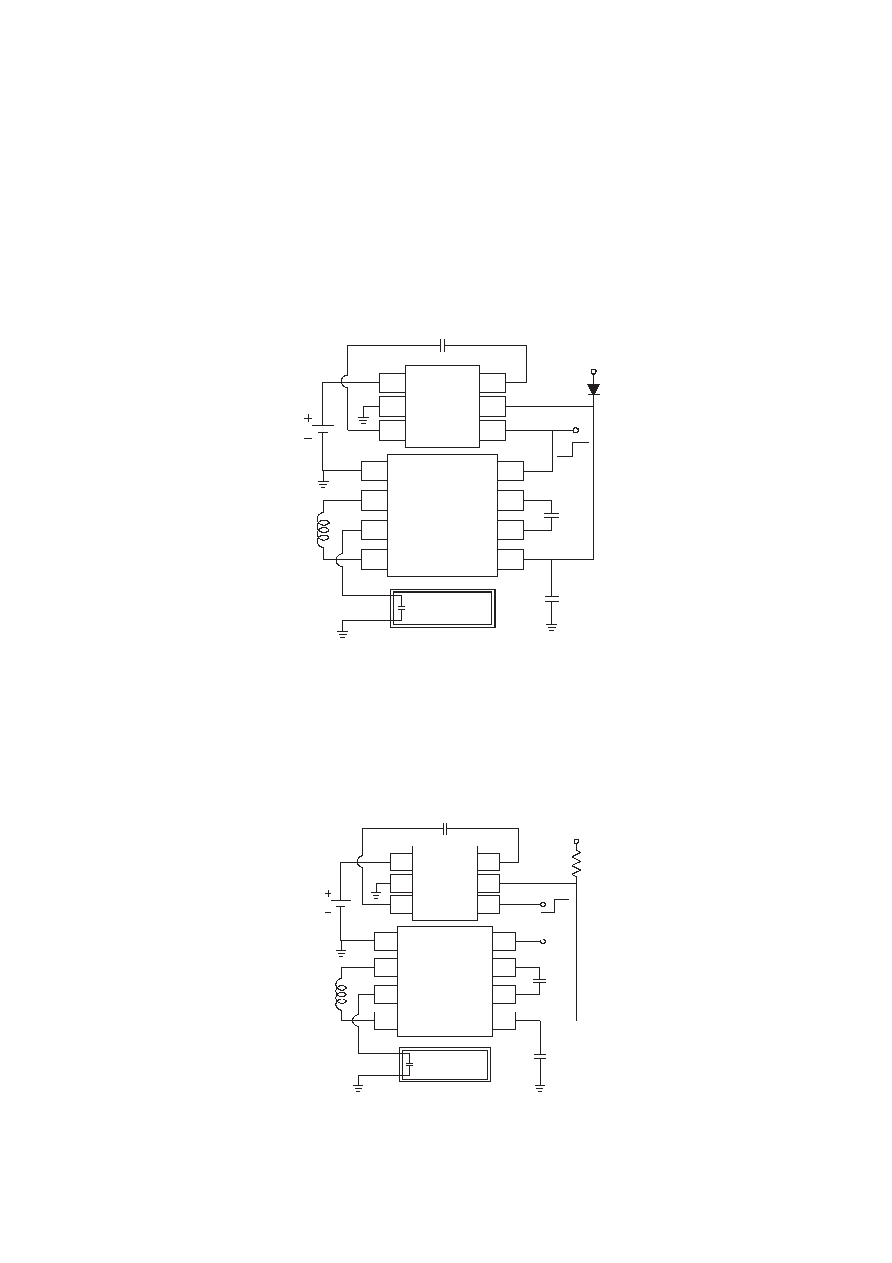
5.0 V PDA
Typical Output
Luminance = 7.7 fL (26.4 cd/m
2
)
Lamp Frequency = 360 Hz
Supply Current = 19 mA
Vout = 220 Vpp
Load = 4 in
2
Durel Æ3 Green EL
1
2
3
4
8
7
6
5
GND
L-
VOUT
L+
E'
CLF2
CLF1
V+
4 in
2
EL Lamp
F
1.0
µ
5.0 mH
Hitachi Metals
MD735L-502A
5.0 V
4.7 nF
D355
ON
GND
5.0V
OFF
6
0
1
2
3
4
5
6
7
8
0
200
400
600
800
1000
Lamp Frequency (Hz)
Designing With D355B
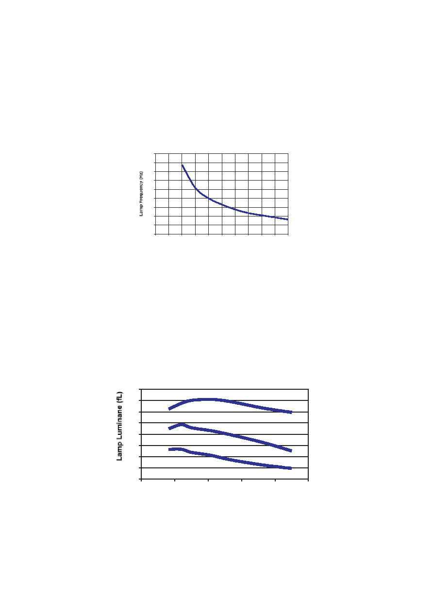
I. Lamp Frequency Capacitor (CLF) Selection
Selecting the appropriate value of capacitor for the low frequency oscillator (CLF) will set the output frequency
of the D355 inverter. Figure 1 graphically represents the inversely proportional relationship between the
CLF capacitor value and the oscillator frequency. In this example at V+=3.0V, LF = 1600 nF-Hz/CLF.
Alternatively, the lamp frequency may also be controlled with an external clock signal with a 50% duty
cycle. The output lamp frequency will be the same frequency as the input clock signal. For example, if a
250Hz input clock signal is used, the resulting lamp frequency will be 250Hz. The clock signal input voltage
should not exceed V+.
The selection of the CLF value can also affect the brightness of the EL lamp because of its control of the
lamp frequency (LF). Although input voltage and lamp size can change EL lamp frequency as well, LF
mainly depends on the CLF value selected or the frequency of the input clock signal to CLF. The luminance
of various sizes of
Durel 3 Blue-green EL lamp driven by a D355B at V+ = 3.0V using the same inductor
value is shown in Figure 2 with respect to lamp frequency.
Figure 1: Typical Lamp Frequency vs. CLF Capacitor
4in
2
EL Lamp
2in
2
EL Lamp
6in
2
EL Lamp
Figure 2: Typical Lamp Luminance vs. Lamp Frequency
0
100
200
300
400
500
600
700
800
900
0
1
2
3
4
5
6
7
8
9
10
CLF (nF)
7
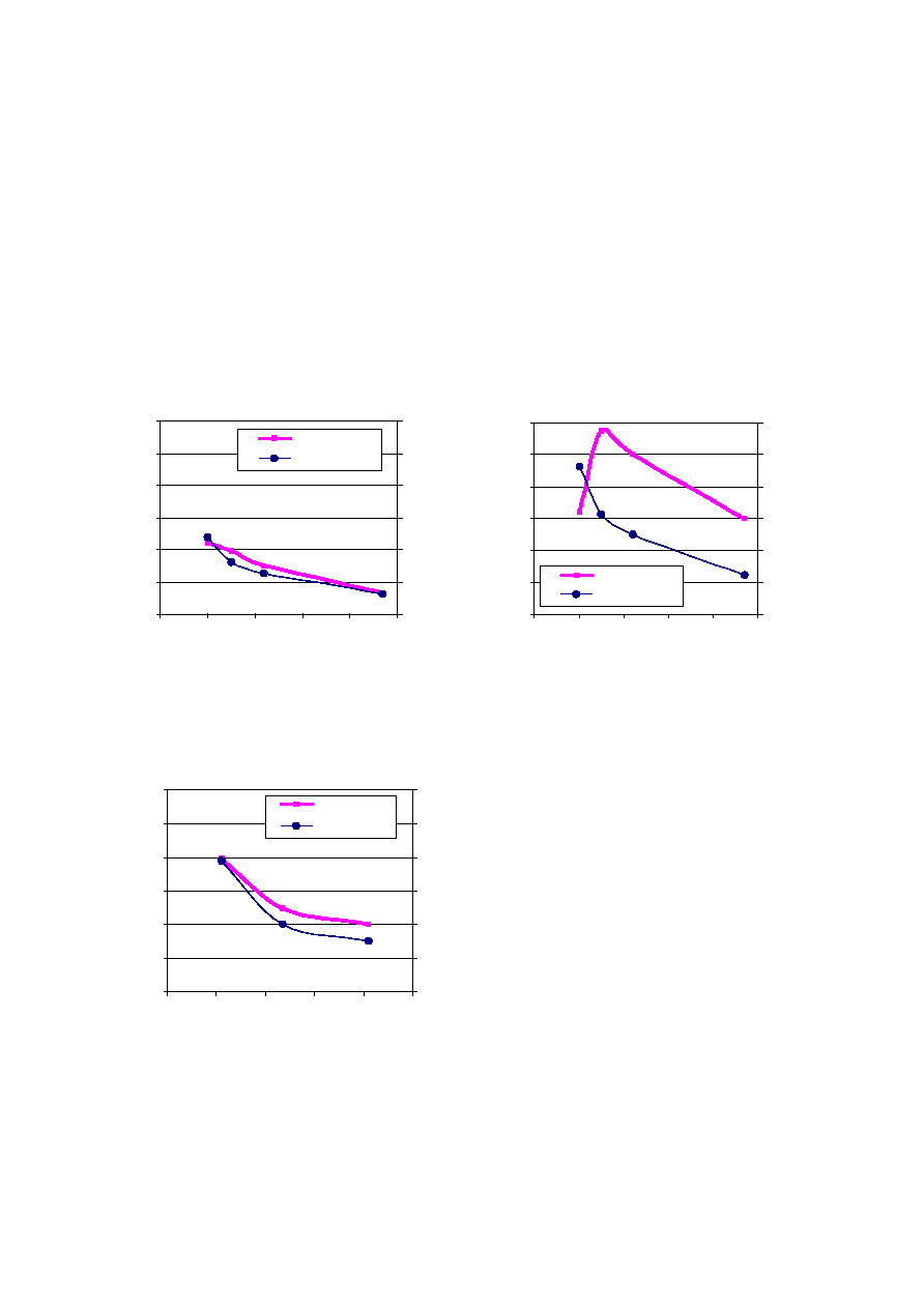
The external inductor (L) selection for a D355B circuit greatly affects the output capability and current draw
of the driver. A careful designer will balance current draw considerations with output performance in the
choice of an ideal inductor for a particular application. Figures 3, 4, and 5 show typical brightness and
current draw of a D355B circuit with different inductor values, lamp sizes, and supply voltages while keeping
the LF constant. Please note that the DC resistance (DCR) of inductors with the same nominal inductance
value may vary with manufacturer and inductor type. Thus, inductors made by a different manufacturer
may yield different outputs, but the trend of the different curves should be similar. Lamp luminance is also
a function of lamp size. In each example, a larger lamp will have less luminance with approximately the
same current draw.
II. Inductor (L) Selection
Figure 3: V+ = 1.5V, 1 in
2
EL Lamp
Figure 4: V+ = 3.0V, 1 in
2
EL Lamp
Figure 5: V+ = 5.0V, 4 in
2
EL Lamp
0
2
4
6
8
10
12
0
1
2
3
4
5
Inductor (mH)
L
a
mp
Lu
mi
na
nc
e
(
f
L
)
0
8
16
24
32
40
48
Cu
r
r
e
n
t
(
m
A)
Brightness
Current
0
2
4
6
8
10
12
0
2
4
6
8
10
Inductor (mH)
L
a
m
p
L
u
m
i
n
an
ce
(fL
)
0
8
16
24
32
40
48
C
u
r
r
e
n
t (m
A
)
Brightness
Current
0
2
4
6
8
10
12
0
1
2
3
4
5
Inductor (mH)
La
m
p
Lum
i
n
a
n
c
e
(
f
L
)
0
8
16
24
32
40
48
Cu
rre
n
t
(
m
A)
Brightness
Current

I. Driving Multi-Segment Lamps
The D355B may be used to drive two or more EL lamps or EL lamp areas independently. An external
switching circuit can be used to turn each lamp segment on or off. A high signal at the E input for the
corresponding EL lamp will power the segment when the IC is enabled. In this example, Segment 1 is
always on when the Durel D355B is enabled. Otherwise, always make sure that at least one segment is
switched on when the driver IC is activated.
8
D355B Design Ideas
II. Enabling the D355B with a High Logic Signal
A low logic signal at the E' pin will enable the D355B. Adding a transistor and two resistors will allow the
D355B to be enabled with a high voltage signal.
1
2
3
4
8
7
6
5
GND
L-
VOUT
L+
E'
CLF2
CLF1
V+
L
V
bat
CLF
D355
EL Lamp
Segment 2
EL Lamp
Segment 1
EL Lamp
Segment 3
1.0
µ
F
OFF
ON
E2
2.2K
4.7K
BAS21LT1
BAS21LT1
MMBT5401LT1
MMBT5551LT1
1K
E3
2.2K
4.7K
BAS21LT1
BAS21LT1
MMBT5401LT1
MMBT5551LT1
1K
OFF
ON
100 nF
100 nF
OFF
ON
1
2
3
4
8
7
6
5
GND
L-
VOUT
L+
E'
CLF2
CLF1
V+
D355
1M
1M
Vbat
EL Lamp
1.0
µ
F
L
CLF
E
Vbat
OFF
ON

III. Two-Level Dimming
Toggle switching between two different EL lamp brightness levels may be achieved with the following
circuit. When DIM is low, the external pnp transistor is saturated and the EL lamp runs at full brightness.
When DIM is high, the external pnp turns off and the 47
resistor reduces the voltage at (V+) and dims the
EL lamp.
9
IV. Lamp Frequency Control with an External Clock Signal
An external clock signal with a 50% duty cycle may be used to control the EL lamp frequency (LF). This
technique allows the designer flexibility to synchronize the El driver IC with other elements in the application.
The output lamp frequency will be the same frequency as the input clock signal. For example, if a 250Hz
input clock signal is used, the resulting lamp frequency will be 250Hz. The clock signal voltage should not
exceed V+.
1
2
3
4
8
7
6
5
GND
L-
VOUT
L+
E'
CLF2
CLF1
V+
EL Lamp
L
V
bat
CLF
D355
47
1k
DIM
1.0
µ
F
2N3906
Low B
High B
E'
OFF
ON
1
2
3
4
8
7
6
5
GND
L-
VOUT
L+
E'
CLF2
CLF1
V+
EL Lamp
L
V
bat
D355
150k
Lamp Frequency CLK
0.2V Max
1.0V Min
1.0
µ
F
OFF
ON
10
V. Automatic Turn-Off After Short Time Delay
It is sometimes desirable for the EL lamp to turn off automatically after a few seconds of operation. Typically,
a mechanical switch pulls E' low to initially turn on the device. When the switch is released, Cdelay keeps
the D355B operating for a short period before turning off. The following table shows typical delay on-
times.
VI. Automatic Turn-Off After Long Time Delay
Longer on-times can be achieved with the addition of an external transistor. Typically, a mechanical switch
pulls E' low to initially turn on the device. When the switch is released, Cdelay keeps the D355B operating
for a period before turning off. The following table shows typical delay on-times using the following circuit
with smaller capacitor values.
Vbat
C
delay
(
µ
F)
1.5V
3.0V
5.0V
5
2.4 s
4.0 s
6.0 s
7
3.3 s
5.5 s
7.8 s
10
5.1 s
8.6 s
12.5 s
15
7.2 s
12.7 s
19.3 s
20
9.9 s
17.2 s
27.0 s
Vbat
C
delay
(
µ
F)
1.5V
3.0V
5.0V
1
9.5 s
13.0 s
15.6 s
2
17.8 s
24.0 s
29.0 s
3
26.5 s
36.0 s
42.0 s
1
2
3
4
8
7
6
5
GND
L-
VOUT
L+
E'
CLF2
CLF1
V+
EL Lamp
L
V
bat
CLF
D355
1M
1.0
µ
F
C
delay
1
2
3
4
8
7
6
5
GND
L-
VOUT
L+
E'
CLF2
CLF1
V+
EL Lamp
L
V
bat
CLF
D355
3.3M
470k
V
bat
1.0
µ
F
C
delay
2N3904
11
VII. High EL Brightness Through Supply Voltage Doubling (Option 1)
Maximum brightness from a D355 is achieved at relatively high supply voltages (>3.0V). An external
voltage boost circuit may be used to increase the voltage supplied to the D355. In the following circuit, the
National Semiconductor LM2665 is used to double the voltage supplied to the D355. This can produce
about twice the brightness of the D355 alone.
NOTE: It is important not to exceed the maximum ratings of either device in this circuit.
2
3
4
7
6
5
L-
VOUT
L+
1
8
GND
E'
CLF2
CLF1
V+
EL Lamp
L
CLF
D355
V
bat
1 V
BAT
3 CAP-
2 GND
CAP+
SD
6
4
5
OUT
V
bat
LM2665
3.3
µ
F
3.3
µ
F
1N914
OFF
ON
In many cases, a resistor may replace the diode in the previous circuit. The diode is used by the LM2665
during startup (see LM2665 datasheet). The circuit below ensures that the LM2665 starts properly before
the D355 is turned on.
NOTE: It is important not to exceed the maximum ratings of either device in this circuit.
VIII. High EL Brightness Through Supply Voltage Doubling (Option 2)
2
3
4
7
6
5
L-
VOUT
L+
1
8
GND
E'
CLF2
CLF1
V+
EL Lamp
L
CLF
D355
V
bat
1 V
BAT
3 CAP-
2 GND
CAP+
SD
6
4
5
OUT
V
bat
270K
V
bat
LM2665
3.3
µ
F
3.3
µ
F
OFF
ON

IX. High EL Brightness Through Supply Voltage Doubling (Option 3)
In the following circuit, the Analog Devices ADM8828 produces a negative Vbat voltage. This voltage may
be connected to the GND pin on the D355 to double the differential voltage supplied to the D355. This can
produce about twice the brightness of the D355 alone.
*NOTE: It is important not to exceed the maximum ratings of either device in this circuit.
X. EL Lamp Brightness Regulation
Regulating the DC supply input voltage to the D355 will result in a constant brightness level from the EL
lamp, regardless of battery voltage. In this example, a Micrel voltage regulator is used.
12
2
3
4
7
6
5
L-
VOUT
L+
1
8
GND
E'
CLF2
CLF1
V+
EL Lamp
L
CLF
D355
1 OUT
3 CAP-
2 IN
CAP+
GND
6
4
5
SHDN
ADM8828
V
bat
1.0
µ
F
1.0
µ
F
OFF
ON
V
bat
1
2
3
4
8
7
6
5
GND
L-
VOUT
L+
E'
CLF2
CLF1
V+
EL Lamp
L
CLF
D355
1.0
µ
F
V
bat
1 GND
2 E
OUT
IN
4
3
MIC5203
E
OFF
ON

XI. High EL Brightness with Parallel D355 Drivers (Option 1)
Two or more D355 EL drivers may be operated in parallel to increase the brightness of the EL lamp by 50-
100%. In this circuit, an external clock signal with a 50% duty cycle is needed to synchronously drive both
D355 ICs. The clock signal voltage should not exceed V+.
Two or more D355 EL drivers may be operated in parallel to increase the brightness of the EL lamp by 50-
100%. In this circuit, two D355 ICs are operating synchronously using their internal oscillators. The lamp
frequency is controlled by a shared CLF capacitor.
XII. High EL Brightness with Parallel D355 Drivers (Option 2)
13
1
2
3
4
8
7
6
5
GND
L-
VOUT
L+
E'
CLF2
CLF1
V+
EL Lamp
L
D355
1
2
3
4
8
7
6
5
GND
L-
VOUT
L+
E'
CLF2
CLF1
V+
L
D355
150k
Lamp Frequency CLK
0.2V Max
1.0V Min
150k
1.0
µ
F
Vbat
OFF
ON
1
2
3
4
8
7
6
5
GND
L-
VOUT
L+
E'
CLF2
CLF1
V+
L
CLF
D355
EL Lamp
1
2
3
4
8
7
6
5
GND
L-
VOUT
L+
E'
CLF2
CLF1
V+
L
D355
100
100
1.0
µ
F
Vbat
OFF
ON
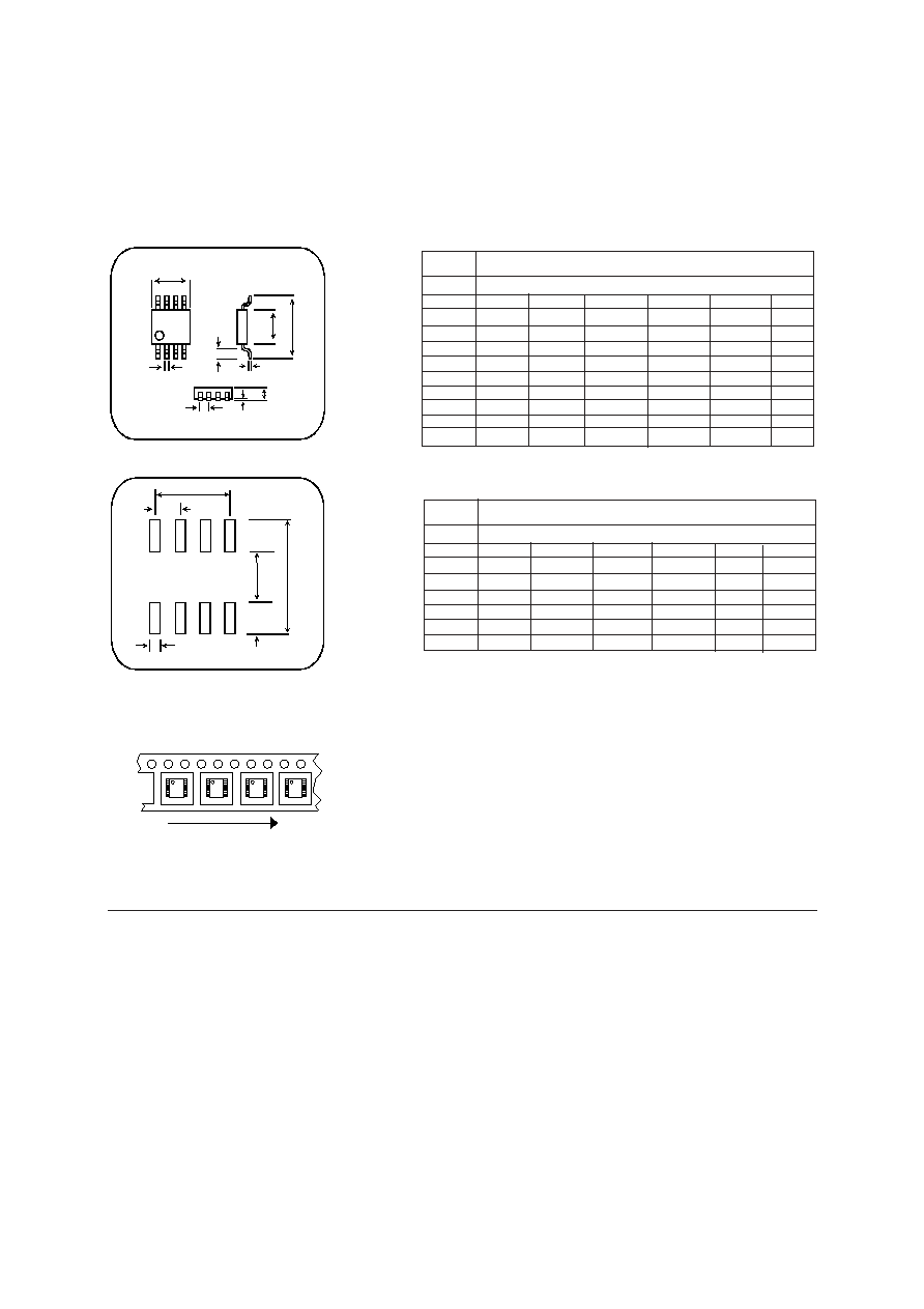
The D355B IC is available as bare die in probed wafer form or in die tray, and in standard MSOP-8 plastic
package per tape and reel. A Durel D355B Designer's Kit (1DDD355BB-K01) provides a vehicle for
evaluating and identifying the optimum component values for any particular application using D355B. Durel
engineers also provide full support to customers, including specialized circuit optimization and application
retrofits.
Ordering Information:
DUREL Corporation
2225 W. Chandler Blvd.
Chandler, AZ 85224-6155
Tel: (480) 917-6000
FAX: (480) 917-6049
Website: http://www.durel.com
© 2000, 2001, 2002 Durel Corporation
Printed in U.S.A.
LIT-I 9034 Rev. A04
The DUREL name and logo are registered trademarks of DUREL CORPORATION.
This information is not intended to and does not create any warranties, express or implied, including any warranty of merchantability or fitness
for a particular purpose. The relative merits of materials for a specific application should be determined by your evaluation.
The EL driver circuits herein are covered by one or more of the following U.S. patents: #5,313,141, #5,347,198, #6,043,610. Corresponding
foreign patents are issued and pending.
ISO 9001 Certified
MSOPs in Tape and Reel: 1DDD355BB-M02
RECOMMENDED PAD LAYOUT
MSOPs are marked with part number (355B) and 3-digit wafer lot code. Bottom
of marking is on the Pin 1 side.
F
H
I
A
B
G
C
D
E
Embossed tape on 360 mm diameter reel per EIA-481-2. 2500 units per
reel. Quantity marked on reel label.
Tape Orientation
e
c
a
b
d
f
A
0.94
0.037
1.02
0.040
1.09
0.043
B
0.05
0.002
0.10
0.004
0.15
0.006
C
0.20
0.008
0.33
0.013
0.46
0.018
D
0.41
0.016
0.53
0.021
0.65
0.026
E
0.13
0.005
0.18
0.007
0.23
0.009
F
2.84
0.112
3.00
0.118
3.15
0.124
G
0.43
0.017
0.65
0.026
0.83
0.033
H
4.70
0.185
4.90
0.193
5.11
0.201
I
2.84
0.112
3.00
0.118
3.25
0.128
Description
mm.
in.
mm.
in.
mm.
in.
MSOP-8
Min.
Typical
Max.
mm.
in.
mm.
in.
mm.
in.
Min.
Typical
Max.
a
0.60
0.0236
0.6
0.0256
0.70
0.0276
b
1.90
0.0748
1.9
0.0768
2.00
0.0788
c
3.3
0.130
3.45
0.136
d
0.89
0.035
0.9
0.038
1.05
0.041
e
5.26
0.207
5.41
0.213
f
0.41
0.016
0.4
0.018
0.51
0.020
MSOP-8 PAD LAYOUT

WWW.ALLDATASHEET.COM
Copyright © Each Manufacturing Company.
All Datasheets cannot be modified without permission.
This datasheet has been download from :
www.AllDataSheet.com
100% Free DataSheet Search Site.
Free Download.
No Register.
Fast Search System.
www.AllDataSheet.com